 | –≠–ª–µ–∫—Ç—Ä–æ–Ω–Ω—ã–π –∫–æ–º–ø–æ–Ω–µ–Ω—Ç: MAX107 | –°–∫–∞—á–∞—Ç—å:  PDF PDF  ZIP ZIP |
General Description
The MAX107 is a dual, 6-bit, analog-to-digital converter
(ADC) designed to allow fast and precise digitizing of in-
phase (I) and quadrature (Q) baseband signals. The
MAX107 converts the analog signals of both I and Q
components to digital outputs at 400Msps while achiev-
ing a signal-to-noise ratio (SNR) of typically 37dB with
an input frequency of 125MHz, and an integral nonlin-
earity (INL) and differential nonlinearity (DNL) of ±0.25
LSB. The MAX107 analog input preamplifiers feature a
400MHz, -0.5dB, and a 1.5GHz, -3dB analog input
bandwidth. Matching channel-to-channel performance
is typically 0.04dB gain, 0.1LSB offset, and 0.2 degrees
phase. Dynamic performance is 36.7dB signal-to-noise
plus distortion (SINAD) with a 125MHz analog input sig-
nal and a sampling speed of 400MHz. A fully differential
comparator design and encoding circuits reduce out-of-
sequence errors, and ensure excellent metastable per-
formance of only one error per 10
16
clock cycles.
In addition, the MAX107 provides LVDS digital outputs
with an internal 6:12 demultiplexer that reduces the out-
put data rate to one-half the sample clock rate. Data is
output in two's complement format. The MAX107 oper-
ates from a +5V analog supply and the LVDS output
ports operate at +3.3V. The data converter's typical
power dissipation is 2.6W. The device is packaged in
an 80-pin, TQFP package with exposed paddle, and is
specified for the extended (-40∞C to +85∞C) tempera-
ture range. For a higher-speed, 800Msps version of the
MAX107, please refer to the MAX105 data sheet.
Applications
VSAT Receivers
WLANs
Test Instrumentation
Communications Systems
Features
o Two Matched 6-Bit, 400Msps ADCs
o Excellent Dynamic Performance
36.7dB SINAD at f
IN
125MHz and
f
CLK
400MHz
o Typical INL and DNL: ±0.25LSB
o Channel-to-Channel Phase Matching: ±0.2∞
o Channel-to-Channel Gain Matching: ±0.04dB
o 6:12 Demultiplexer reduces the Data Rates to
200MHz
o Low Error Rate: 10
16
Metastable States at
400Msps
o LVDS Digital Outputs in Two's Complement
Format
MAX107
Dual, 6-Bit, 400Msps ADC with On-Chip,
Wideband Input Amplifier
________________________________________________________________ Maxim Integrated Products
1
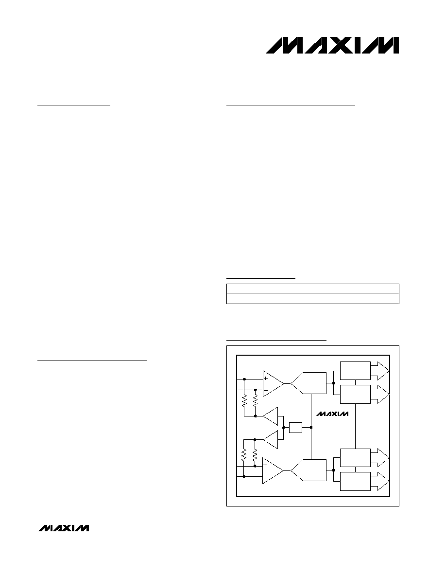
REF
I
PRIMARY
PORT
I
AUXILIARY
PORT
Q
PRIMARY
PORT
Q
AUXILIARY
PORT
I ADC
Q ADC
MAX107
Block Diagram
19-2007; Rev 0; 5/01
Ordering Information
PART
TEMP. RANGE
PIN-PACKAGE
MAX107ECS
-40∞C to +85∞C
80-Pin TQFP-EP
Pin Configuration appears at end of data sheet.
For pricing, delivery, and ordering information, please contact Maxim/Dallas Direct! at
1-888-629-4642, or visit Maxim's website at www.maxim-ic.com.

MAX107
Dual, 6-Bit, 400Msps ADC with On-Chip,
Wideband Input Amplifier
2
_______________________________________________________________________________________
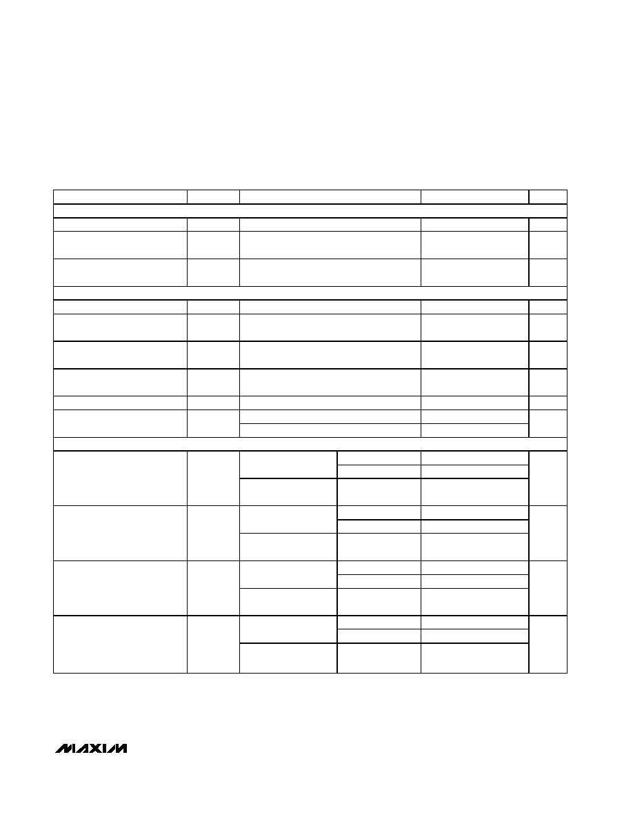
ABSOLUTE MAXIMUM RATINGS
Stresses beyond those listed under "Absolute Maximum Ratings" may cause permanent damage to the device. These are stress ratings only, and functional
operation of the device at these or any other conditions beyond those indicated in the operational sections of the specifications is not implied. Exposure to
absolute maximum rating conditions for extended periods may affect device reliability.
AV
CC
, AV
CC
I, AV
CC
Q and AV
CC
R to AGND............-0.3V to +6V
OV
CC
I and OV
CC
Q to OGND ...................................-0.3V to +4V
AGND to OGND ................................................... -0.3V to +0.3V
P0I± to P5I± and A0I± to A5I±
DREADY+, DREADY- to OGNDI ..............-0.3V to OV
CC
I+0.3V
P0Q± to P5Q±, A0Q± to A5Q±
DOR+ and DOR- to OGNDQ .................-0.3V to OV
CC
Q+0.3V
REF to AGNDR...........................................-0.3V to AV
CC
R+0.3V
Differential Voltage Between INI+ and INI- ....................-2V, +2V
Differential Voltage Between INQ+ and INQ-.................-2V, +2V
Differential Voltage Between CLK+ and CLK- ...............-2V, +2V
Maximum Current Into Any Pin ...........................................50mA
Continuous Power Dissipation (T
A
= +70∞C)
80-Pin TQFP (derate 44mW/∞C above +70∞C)..................3.5W
Operating Temperature Range
MAX107ECS .....................................................-40∞C to +85∞C
Junction Temperature ......................................................+150∞C
Storage Temperature Range .............................-60∞C to +150∞C
Lead temperature (soldering, 10s) ..................................+300∞C
ELECTRICAL CHARACTERISTICS
(AV
CC
= AV
CC
I = AV
CC
Q = AV
CC
R = +5V, OV
CC
I = OV
CC
Q = +3.3V, AGND = AGNDI = AGNDQ = AGNDR = 0, OGNDI = OGNDQ
= 0, f
CLK
= 401.408MHz, C
L
= 1µF to AGND at REF, R
L
= 100
±1% applied to digital LVDS outputs, T
A
= T
MIN
to T
MAX
, unless
otherwise noted. Typical values are at T
A
= +25
∞C)
PARAMETER
SYMBOL
CONDITIONS
MIN
TYP
MAX
UNITS
DC ACCURACY
Resolution
RES
6
Bits
Integral Nonlinearity (Note 1)
INL
-1
±0.2
1
LSB
Differential Nonlinearity
(Note 1)
DNL
No missing codes guaranteed
-1
±0.25
1
LSB
Offset Voltage
V
OS
(Note 2)
-1
±0.25
1
LSB
O ffset M atchi ng Betw een AD C s
OM
(Note 2)
-0.5
±0.1
0.5
LSB
ANALOG INPUTS (INI+, INI-, INQ+, INQ-)
Input Open-Circuit Voltage
V
AOC
2.4
2.5
2.6
V
Input Open-Circuit Voltage
Matching
(V
INI+
- V
IN-
) - (V
INQ+
- V
INQ-
)
±7.5
mV
Common Mode Input Voltage
Range (Note 3)
V
CM
Signal + Offset w.r.t. AGND
1.85
3.05
V
Full-Scale Analog Input
Voltage Range (Note 4)
V
FSR
0.76
0.8
0.84
Vp-p
Input Resistance
R
IN
1.7
2
k
Input Capacitance
C
IN
1.5
pF
Input Resistance Temperature
Coefficient
TCR
IN
150
ppm/
∞C
Full-Power Analog Input BW
FPBW
-0.5dB
400
MHz
REFERENCE OUTPUT
Reference Output Resistance
R
REF
Referenced to AGNDR
5
Reference Output Voltage
V
REF
I
SOURCE
= 500
µA
2.45
2.50
2.55
V
MAX107
Dual, 6-Bit, 400Msps ADC with On-Chip,
Wideband Input Amplifier
_______________________________________________________________________________________
3
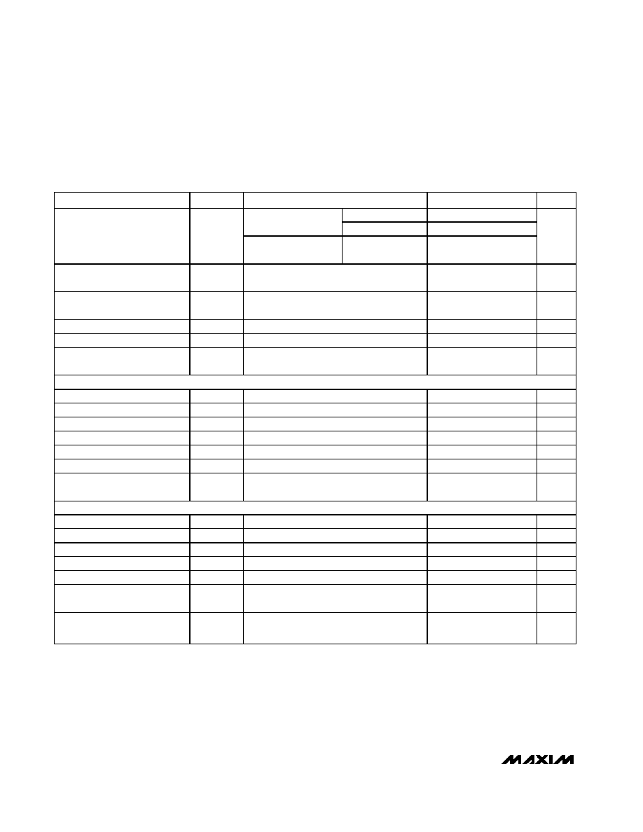
ELECTRICAL CHARACTERISTICS (continued)
(AV
CC
= AV
CC
I = AV
CC
Q = AV
CC
R = +5V, OV
CC
I = OV
CC
Q = +3.3V, AGND = AGNDI = AGNDQ = AGNDR = 0, OGNDI = OGNDQ
= 0, f
CLK
= 401.408MHz, C
L
= 1µF to AGND at REF, R
L
= 100
±1% applied to digital LVDS outputs, T
A
= T
MIN
to T
MAX
, unless
otherwise noted. Typical values are at T
A
= +25
∞C)
PARAMETER
SYMBOL
CONDITIONS
MIN
TYP
MAX
UNITS
CLOCK INPUTS (CLK+, CLK-)
Clock Input Resistance
R
CLK
CLK+ and CLK- to AGND
5
k
Clock Input Resistance
Temperature Coefficient
TCR
CLK
150
ppm/
∞C
Minimum Clock Input
Amplitude
500
mVp-p
LVDS OUTPUTS (P0I
± TO P5I±, P0Q± TO P5Q±, A0I± TO A5I±, A0Q± TO A5Q±, DREADY+, DREADY-, DOR+, DOR-)
Differential Output Voltage
V
OD
247
400
mV
C hang e i n M ag ni tud e of
V
OD
Betw een "0" and "1" S tates
V
OD
±25
mV
Steady-State Common Mode
Output Voltage
V
OC(SS)
1.125
1.375
V
Change in Magnitude of V
OC
Between "0" and "1" States
V
OC
±25
mV
Differential Output Resistance
80
160
Short output together
2.5
Output Current
Short to OGNDI = OGNDQ
25
mA
DYNAMIC SPECIFICATION
Differential
5.4
5.9
f
IN
= 124.999MHz at
-0.5dB FS (Note 9)
Single-ended
5.9
Effective Number of Bits
(Note 8)
ENOB
f
IN
= 200.067MHz at
-0.5dB FS
Differential
5.75
Bits
Differential
35
37
f
IN
= 124.999MHz at
-0.5dB FS (Note 9)
Single-ended
37
Signal-to-Noise Ratio
(Notes 10, 11)
SNR
f
IN
= 200.067MHz at
-0.5dB FS
Differential
36.6
dB
Differential
-49.5
-42
f
IN
= 124.999MHz at
-0.5dB FS (Note 9)
Single-ended
-49.5
Total Harmonic Distortion
(Note 11)
THD
f
IN
= 200.067MHz at
-0.5dB FS
Differential
-44.5
dBc
Differential
43
51
f
IN
= 124.999MHz at
-0.5dB FS (Note 9)
Single-ended
51
Spurious-Free Dynamic Range
SFDR
f
IN
= 200.067MHz at
-0.5dB FS
Differential
45.5
dB
MAX107
Dual, 6-Bit, 400Msps ADC with On-Chip,
Wideband Input Amplifier
4
_______________________________________________________________________________________
ELECTRICAL CHARACTERISTICS (continued)
(AV
CC
= AV
CC
I = AV
CC
Q = AV
CC
R = +5V, OV
CC
I = OV
CC
Q = +3.3V, AGND = AGNDI = AGNDQ = AGNDR = 0, OGNDI = OGNDQ
= 0, f
CLK
= 401.408MHz, C
L
= 1µF to AGND at REF, R
L
= 100
±1% applied to digital LVDS outputs, T
A
= T
MIN
to T
MAX
, unless
otherwise noted. Typical values are at T
A
= +25
∞C)
PARAMETER
SYMBOL
CONDITIONS
MIN
TYP
MAX
UNITS
Differential
35
36.7
f
IN
= 124.999MHz at
-0.5dB FS (Note 9)
Single-ended
36.7
Signal-to-Noise Plus Distortion
Ratio
SINAD
f
IN
= 200.067MHz at
-0.5dB FS
Differential
36
dB
Two-Tone Intermodulation
TTIMD
f
IN1
= 100.009MHz, f
IN2
= 102.067MHz at
-7dBFS
-55
dBc
Crosstalk Between ADCs
XTLK
f
INI
= 200.0180MHz, f
INQ
= 210.0140MHz
at -0.5dB FS
-70
dB
Gain Match Between ADCs
GM
(Note 12)
-0.3
±0.04
+0.3
dB
Phase Match Between ADCs
PM
(Note 12)
-2
±0.2
+2
deg
Metastable Error Rate
Less than 1 in 10
16
Clock
Cycles
POWER REQUIREMENTS
Analog Supply Voltage
AV
CC_
AV
CC
= AV
CC
I = AV
CC
Q = AV
CC
R
5
±5%
V
Digital Supply Voltage
OV
CC_
OV
CC
I = OV
CC
Q
3.3
±10%
V
Analog Supply Current
I
CC
I
CC
= AI
CC
R + AI
CC
I + AI
CC
Q + AI
CC
250
320
mA
Output Supply Current
OI
CC
OI
CC
= OI
CC
I + OI
CC
Q
400
510
mA
Analog Power Dissipation
P
DISS
2.6
W
C om m on- M od e Rej ecti on Rati o
CMRR
V
IN_+
= V
IN_-
=
±0.1V (Note 6)
40
60
dB
Power-Supply Rejection Ratio
PSRR
AV
CC
= AV
CC
I = AV
CC
Q = AV
CC
R =
+4.75V to +5.25V (Note 7)
40
57
dB
TIMING CHARACTERISTICS
Maximum Sample Rate
f
MAX
400
Msps
Clock Pulse Width Low
t
PWL
1.25
ns
Clock Pulse Width High
t
PWH
1.25
ns
Aperture Delay
t
AD
100
ps
Aperture Jitter
t
AJ
1.5
ps
RMS
CLK-to-DREADY Propagation
Delay
t
PD1
(Note 13)
1.5
ns
DREADY-to-DATA
Propagation Delay
t
PD2
(Notes 5, 13)
0
120
300
ps

MAX107
Dual, 6-Bit, 400Msps ADC with On-Chip,
Wideband Input Amplifier
_______________________________________________________________________________________
5
Note 1:
INL and DNL is measured using a sine-histogram method.
Note 2:
Input offset is the voltage required to cause a transition between codes 0 and -1.
Note 3:
Numbers provided are for DC-coupled case. The user has the choice of AC-coupling, in which case, the DC input voltage
level does not matter.
Note 4:
The peak-to-peak input voltage required, causing a full-scale digitized output when using a trigonometric curve-fitting algo
rithm (e.g. FFT).
Note 5:
Guaranteed by design and characterization.
Note 6:
Common-mode rejection ratio is defined as the ratio of the change in the offset voltage to the change in the common-mode
voltage expressed in dB.
Note 7:
Measured with analog power supplies tied to the same potential.
Note 8:
Effective number of bits (ENOB) is computed from a curve-fit referenced to the theoretical full-scale range.
Note 9:
The clock and input frequencies are chosen so that there are 2041 cycles in an 8,192-long record.
Note 10: Signal-to-noise-ratio (SNR) is measured both with the other channel idling and converting an out-of-phase signal.
The worst case number is presented. Harmonic distortion components two through five are excluded from the noise.
Note 11: Harmonic distortion components two through five are included in the total harmonic distortion specification.
Note 12: Both I and Q inputs are effectively tied together (e.g. driven by power splitter). Signal amplitude is -0.5dB FS at an input
frequency of f
IN
= 124.999 MHz.
Note 13: Measured with a differential probe, 1pF capacitance.
ELECTRICAL CHARACTERISTICS (continued)
(AV
CC
= AV
CC
I = AV
CC
Q = AV
CC
R = +5V, OV
CC
I = OV
CC
Q = +3.3V, AGND = AGNDI = AGNDQ = AGNDR = 0, OGNDI = OGNDQ
= 0, f
CLK
= 401.408MHz, C
L
= 1µF to AGND at REF, R
L
= 100
±1% applied to digital LVDS outputs, T
A
= T
MIN
to T
MAX
, unless
otherwise noted. Typical values are at T
A
= +25
∞C)
PARAMETER
SYMBOL
CONDITIONS
MIN
TYP
MAX
UNITS
DREADY Duty Cycle
(Notes 5, 13)
47
53
%
LVDS Output Rise-Time
t
RDATA
20% to 80% (Notes 5, 13)
200
500
ps
LVDS Output Fall-Time
t
FDATA
20% to 80% (Notes 5, 13)
200
500
ps
Any differential pair
<65
LVDS Differential Skew
t
SKEW1
Any tw o LV D S outp ut si g nal s excep t D RE AD Y <100
ps
DREADY Rise-Time
t
RDREADY
20% to 80% (Notes 5, 13)
200
500
ps
DREADY Fall-Time
t
FDREADY
20% to 80% (Notes 5, 13)
200
500
ps
Primary Port Pipeline Delay
t
PDP
5
Clock
Cycles
Auxiliary Port Pipeline Delay
t
PDA
6
Clock
Cycles