 | ÐлекÑÑоннÑй компоненÑ: MAX1072 | СкаÑаÑÑ:  PDF PDF  ZIP ZIP |
Äîêóìåíòàöèÿ è îïèñàíèÿ www.docs.chipfind.ru
General Description
The MAX1072/MAX1075 low-power, high-speed, serial-
output, 10-bit, analog-to-digital converters (ADCs) oper-
ate at up to 1.8Msps. These devices feature true-differen-
tial inputs, offering better noise immunity, distortion
improvements, and a wider dynamic range over single-
ended inputs. A standard SPITM/QSPITM/MICROWIRETM
interface provides the clock necessary for conversion.
These devices easily interface with standard digital signal
processor (DSP) synchronous serial interfaces.
The MAX1072/MAX1075 operate from a single +4.75V to
+5.25V supply voltage and require an external reference.
The MAX1072 has a unipolar analog input, while the
MAX1075 has a bipolar analog input. These devices fea-
ture a partial power-down mode and a full power-down
mode for use between conversions, which lower the sup-
ply current to 1mA (typ) and 1µA (max), respectively. Also
featured is a separate power-supply input (V
L
), which
allows direct interfacing to +1.8V to V
DD
digital logic. The
fast conversion speed, low-power dissipation, excellent
AC performance, and DC accuracy (
±
0.5 LSB INL) make
the MAX1072/MAX1075 ideal for industrial process con-
trol, motor control, and base-station applications.
The MAX1072/MAX1075 come in a 12-pin TQFN pack-
age, and are available in the commercial (0°C to +70°C)
and extended (-40°C to +85°C) temperature ranges.
Applications
Data Acquisition
Bill Validation
Motor Control
Communications
Portable Instruments
Features
o
1.8Msps Sampling Rate
o
Only 45mW (typ) Power Dissipation
o
Only 1µA (max) Shutdown Current
o
High-Speed, SPI-Compatible, 3-Wire Serial Interface
o
61dB S/(N + D) at 525kHz Input Frequency
o
Internal True-Differential Track/Hold (T/H)
o
External Reference
o
No Pipeline Delays
o
Small 12-Pin TQFN Package
MAX1072/MAX1075
1.8Msps, Single-Supply, Low-Power,
True-Differential, 10-Bit ADCs
________________________________________________________________ Maxim Integrated Products
1
12
AIN+
11
N.C.
10
SCLK
4
5
N.C.
6
GND
1
2
REF
3
9
8
7
RGND
CNVST
DOUT
V
L
MAX1072
MAX1075
AIN-
V
DD
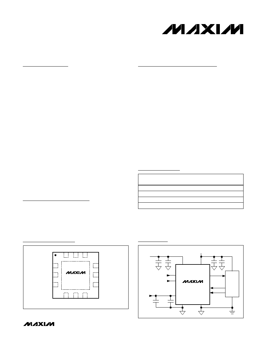
TQFN
TOP VIEW
PART
TEMP RANGE
PIN-
PACKAGE
INPUT
MAX1072
CTC-T
0
°
C to +70
°
C
12 TQFN-12
Unipolar
MAX1072ETC-T
-40
°
C to +85
°
C
12 TQFN-12
Unipolar
MAX1075
CTC-T
0
°
C to +70
°
C
12 TQFN-12
Bipolar
MAX1075ETC-T
-40
°
C to +85
°
C
12 TQFN-12
Bipolar
Pin Configuration
Ordering Information
MAX1072
MAX1075
DOUT
AIN+
REF
4.7
µ
F
10
µ
F
10
µ
F
+4.75V TO +5.25V
0.01
µ
F
0.01
µ
F
0.01
µ
F
+1.8V TO V
DD
AIN-
REF
V
DD
DIFFERENTIAL
INPUT
VOLTAGE
RGND
V
L
GND
CNVST
SCLK
µ
C/DSP
+
-
Typical Operating Circuit
19-3153; Rev 0; 1/04
For pricing, delivery, and ordering information, please contact Maxim/Dallas Direct! at
1-888-629-4642, or visit Maxim's website at www.maxim-ic.com.
SPI/QSPI are trademarks of Motorola, Inc.
MICROWIRE is a trademark of National Semiconductor Corp.
MAX1072/MAX1075
1.8Msps, Single-Supply, Low-Power,
True-Differential, 10-Bit ADCs
2
_______________________________________________________________________________________
ABSOLUTE MAXIMUM RATINGS
ELECTRICAL CHARACTERISTICS
(V
DD
= +5V ±5%, V
L
= V
DD
, V
REF
= 4.096V, f
SCLK
= 28.8MHz, 50% duty cycle, T
A
= T
MIN
to T
MAX
, unless otherwise noted. Typical
values are at T
A
= +25°C.)
Stresses beyond those listed under "Absolute Maximum Ratings" may cause permanent damage to the device. These are stress ratings only, and functional
operation of the device at these or any other conditions beyond those indicated in the operational sections of the specifications is not implied. Exposure to
absolute maximum rating conditions for extended periods may affect device reliability.
V
DD
to GND ..............................................................-0.3V to +6V
V
L
to GND ...................-0.3V to the lower of (V
DD
+ 0.3V) or +6V
Digital Inputs
to GND ....................-0.3V to the lower of (V
DD
+ 0.3V) or +6V
Digital Output
to GND .......................-0.3V to the lower of (V
L
+ 0.3V) or +6V
Analog Inputs and
REF to GND.............-0.3V to the lower of (V
DD
+ 0.3V) or +6V
RGND to GND .......................................................-0.3V to +0.3V
Maximum Current into Any Pin............................................50mA
Continuous Power Dissipation (T
A
= +70°C)
12-Pin TQFN (derate 16.9mW/°C above +70°C) ......1349mW
Operating Temperature Ranges
MAX107_ CTC ...................................................0°C to +70°C
MAX107_ ETC.................................................-40°C to +85°C
Junction Temperature ......................................................+150°C
Storage Temperature Range .............................-60°C to +150°C
Lead Temperature (soldering, 10s) .................................+300°C
PARAMETER
SYMBOL
CONDITIONS
MIN
TYP
MAX
UNITS
DC ACCURACY
Resolution
10
Bits
Relative Accuracy
INL
(Note 1)
±0.5
LSB
Differential Nonlinearity
DNL
(Note 2)
±0.5
LSB
Offset Error
±2
LSB
Offset-Error Temperature
Coefficient
±1
ppm/°C
Gain Error
Offset nulled
±2
LSB
Gain Temperature Coefficient
±2
ppm/°C
DYNAMIC SPECIFICATIONS
(f
IN
= 525kHz
sine wave
, V
IN
= V
REF
, unless otherwise noted.)
Signal-to-Noise Plus Distortion
SINAD
60
61
dB
Total Harmonic Distortion
THD
-80
-74
dB
Spurious-Free Dynamic Range
SFDR
-80
-74
dB
Intermodulation Distortion
IMD
f
IN1
= 250kHz, f
IN2
= 300kHz
-78
dB
Full-Power Bandwidth
-3dB point, small-signal method
20
MHz
Full-Linear Bandwidth
S/(N + D)
56dB, single ended
2
MHz
CONVERSION RATE
Minimum Conversion Time
t
CONV
(Note 3)
0.556
µs
Maximum Throughput Rate
1.8
Msps
M i ni m um Thr oug hp ut Rate
( N ote 4)
10
ksps
Track-and-Hold Acquisition Time
t
ACQ
(Note 5)
104
ns
Aperture Delay
5
ns
Aperture Jitter
(Note 6)
30
ps
External Clock Frequency
f
SCLK
28.8
MHz
MAX1072/MAX1075
1.8Msps, Single-Supply, Low-Power,
True-Differential, 10-Bit ADCs
_______________________________________________________________________________________
3
ELECTRICAL CHARACTERISTICS (continued)
(V
DD
= +5V ±5%, V
L
= V
DD
, V
REF
= 4.096V, f
SCLK
= 28.8MHz, 50% duty cycle, T
A
= T
MIN
to T
MAX
, unless otherwise noted. Typical
values are at T
A
= +25°C.)
PARAMETER
SYMBOL
CONDITIONS
MIN
TYP
MAX
UNITS
ANALOG INPUTS (AIN+, AIN-)
AIN+ - AIN-, MAX1072
0
V
REF
Differential Input Voltage Range
V
IN
AIN+ - AIN-, MAX1075
-V
REF
/ 2
+V
REF
/ 2
V
Absolute Input Voltage Range
0
V
DD
V
DC Leakage Current
±1
µA
Input Capacitance
Per input pin
20
pF
Input Current (Average)
Time averaged at maximum throughput rate
75
µA
REFERENCE INPUT (REF)
REF Input Voltage Range
V
REF
1.0
V
DD
+
50mV
V
Input Capacitance
20
pF
DC Leakage Current
±1
µA
Input Current (Average)
Time averaged at maximum throughput rate
400
µA
DIGITAL INPUTS (SCLK, CNVST)
Input Voltage Low
VIL
0.3 x V
L
V
Input Voltage High
VIH
0.7 x V
L
V
Input Leakage Current
I
IL
0.05
±10
µA
DIGITAL OUTPUT (DOUT)
Output Load Capacitance
C
OUT
For stated timing performance
30
pF
Output Voltage Low
V
OL
I
SINK
= 5mA, V
L
1.8V
0.4
V
Output Voltage High
V
OH
I
SOURCE
= 1mA, V
L
1.8V
V
L
- 0.5V
V
Output Leakage Current
I
OL
Output high impedance
±0.2
±10
µA
POWER REQUIREMENTS
Analog Supply Voltage
V
DD
4.75
5.25
V
Digital Supply Voltage
V
L
1.8
V
DD
V
Static, f
SCLK
= 28.8MHz
7
9
Static, no SCLK
4
5
Analog Supply Current,
Normal Mode
I
DD
Operational,
1.8Msps
9
11
mA
f
SCLK
= 28.8MHz
1
Analog Supply Current,
Partial Power-Down Mode
I
DD
No SCLK
1
mA
f
SCLK
= 28.8MHz
1
Analog Supply Current,
Full Power-Down Mode
I
DD
No SCLK
1
µA
Operational, full-scale input at 1.8Msps
1
2.5
Static, f
SCLK
= 28.8MHz
0.4
1
Partial/full power-down mode,
f
SCLK
= 28.8MHz
0.2
0.5
mA
Digital Supply Current (Note 7)
Static, no SCLK (all modes)
0.1
1
µA
Positive-Supply Rejection
PSR
V
DD
= 5V ±5%, full-scale input
±0.2
±3.0
mV
MAX1072/MAX1075
1.8Msps, Single-Supply, Low-Power,
True-Differential, 10-Bit ADCs
4
_______________________________________________________________________________________
Note 1:
Relative accuracy is the deviation of the analog value at any code from its theoretical value after the gain error and the offset
error have been nulled.
Note 2:
No missing codes over temperature.
Note 3:
Conversion time is defined as the number of clock cycles (16) multiplied by the clock period.
Note 4:
At sample rates below 10ksps, the input full-linear bandwidth is reduced to 5kHz.
Note 5:
The listed value of three SCLK cycles is given for full-speed continuous conversions. Acquisition time begins on the 14th ris-
ing edge of SCLK and terminates on the next falling edge of CNST. The IC idles in acquisition mode between conversions.
Note 6:
Undersampling at the maximum signal bandwidth requires the minimum jitter spec for SINAD performance.
Note 7:
Digital supply current is measured with the V
IH
level equal to V
L
, and the V
IL
level equal to GND.
TIMING CHARACTERISTICS
(V
DD
= +5V ±5%, V
L
= V
DD
, V
REF
= 4.096V, f
SCLK
= 28.8MHz, 50% duty cycle, T
A
= T
MIN
to T
MAX
, unless otherwise noted. Typical
values are at T
A
= +25°C.)
PARAMETER
SYMBOL
CONDITIONS
MIN
TYP
MAX
UNITS
SCLK Pulse-Width High
t
CH
V
L
= 1.8V to V
DD
15.6
ns
SCLK Pulse-Width Low
t
CL
V
L
= 1.8V to V
DD
15.6
ns
C
L
= 30pF, V
L
= 4.75V to V
DD
14
C
L
= 30pF, V
L
= 2.7V to V
DD
17
SCLK Rise to DOUT Transition
t
DOUT
C
L
= 30pF, V
L
= 1.8V to V
DD
24
ns
DOUT Remains Valid After SCLK
t
DHOLD
V
L
= 1.8V to V
DD
4
ns
CNVST Fall to SCLK Fall
t
SETUP
V
L
= 1.8V to V
DD
10
ns
CNVST Pulse Width
t
CSW
V
L
= 1.8V to V
DD
20
ns
Power-Up Time; Full Power-Down
T
PWR-UP
2
ms
Restart Time; Partial Power-Down
t
RCV
16
Cycles
CNVST
SCLK
DOUT
t
DHOLD
t
DOUT
t
SETUP
t
CSW
t
CL
t
CH
Figure 1. Detailed Serial-Interface Timing
GND
6k
C
L
DOUT
DOUT
C
L
GND
V
L
a) HIGH-Z TO V
OH
, V
OL
TO V
OH
,
AND V
OH
TO HIGH-Z
b) HIGH-Z TO V
OL
, V
OH
TO V
OL
,
AND V
OL
TO HIGH-Z
6k
Figure 2. Load Circuits for Enable/Disable Times
MAX1072/MAX1075
1.8Msps, Single-Supply, Low-Power,
True-Differential, 10-Bit ADCs
_______________________________________________________________________________________
5
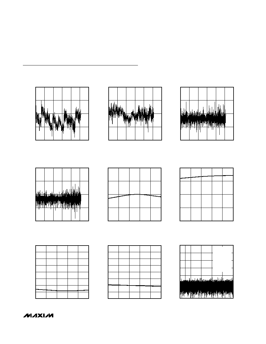
Typical Operating Characteristics
(V
DD
= +5V, V
L
= V
DD
, V
REF
= 4.096V, f
SCLK
= 28.8MHz, T
A
= T
MIN
to T
MAX
, unless otherwise noted. Typical values are at T
A
= +25°C.)
INTEGRAL NONLINEARITY
vs. DIGITAL OUTPUT CODE (MAX1072)
MAX1072/75 toc01
DIGITAL OUTPUT CODE
INL (LSB)
1000
800
600
400
200
-0.1
0
0.1
0.2
-0.2
0
1200
INTEGRAL NONLINEARITY
vs. DIGITAL OUTPUT CODE (MAX1075)
MAX1072/75 toc02
DIGITAL OUTPUT CODE
INL (LSB)
1000
800
600
400
200
-0.1
0
0.1
0.2
-0.2
0
1200
DIFFERENTIAL NONLINEARITY
vs. DIGITAL OUTPUT CODE (MAX1072)
MAX1072/75 toc03
DIGITAL OUTPUT CODE
DNL (LSB)
1000
800
600
400
200
-0.1
0
0.1
0.2
-0.2
0
1200
DIFFERENTIAL NONLINEARITY
vs. DIGITAL OUTPUT CODE (MAX1075)
MAX1072/75 toc04
DIGITAL OUTPUT CODE
DNL (LSB)
1000
800
600
400
200
-0.1
0
0.1
0.2
-0.2
0
1200
OFFSET ERROR
vs. TEMPERATURE (MAX1072)
MAX1072/75 toc05
TEMPERATURE (
°
C)
OFFSET ERROR (LSB)
60
35
10
-15
-0.25
0
0.25
0.50
-0.50
-40
85
OFFSET ERROR
vs. TEMPERATURE (MAX1075)
MAX1072/75 toc06
TEMPERATURE (
°
C)
OFFSET ERROR (LSB)
60
35
10
-15
-0.25
0
0.25
0.50
-0.50
-40
85
GAIN ERROR
vs. TEMPERATURE (MAX1072)
MAX1072/75 toc07
TEMPERATURE (
°
C)
GAIN ERROR (LSB)
60
35
-15
10
-0.75
-0.50
-0.25
0
0.25
0.50
0.75
1.00
-1.00
-40
85
GAIN ERROR
vs. TEMPERATURE (MAX1075)
MAX1072/75 toc08
TEMPERATURE (
°
C)
GAIN ERROR (LSB)
60
35
-15
10
-0.75
-0.50
-0.25
0
0.25
0.50
0.75
1.00
-1.00
-40
85
FFT PLOT (MAX1072)
MAX1072/75 toc09
ANALOG INPUT FREQUENCY (kHz)
AMPLITUDE (dB)
800
600
400
200
-120
-100
-80
-60
-40
-20
0
-140
0
1000
f
SAMPLE
= 2Msps
f
SCLK
= 32MHz
f
IN
= 100kHz
SINAD = 61.4dB
SNR = 61.4dB
THD = -94.42dB
SFDR = 84.54dB