Äîêóìåíòàöèÿ è îïèñàíèÿ www.docs.chipfind.ru
General Description
The MAX1086MAX1089 are low-cost, micropower, ser-
ial output 10-bit analog-to-digital converters (ADCs)
available in a tiny 8-pin SOT23. The MAX1086/MAX1088
operate with a single +5V supply. The MAX1087/MAX1089
operate with a single +3V supply. The devices feature a
successive-approximation ADC, automatic shutdown,
fast wake-up (1.4µs), and a high-speed 3-wire inter-
face. Power consumption is only 0.5mW (V
DD
= +2.7V)
at the maximum sampling rate of 150ksps.
AutoshutdownTM (0.1µA) between conversions results in
reduced power consumption at slower throughput
rates.
The MAX1086/MAX1087 provide 2-channel, single-
ended operation and accept input signals from 0 to
V
REF
. The MAX1088/MAX1089 accept true-differential
inputs ranging from 0 to V
REF
. Data is accessed using
an external clock through the 3-wire SPITM, QSPITM, and
MICROWIRETMcompatible serial interface. Excellent
dynamic performance, low-power, ease of use, and
small package size, make these converters ideal for
portable battery-powered data acquisition applications,
and for other applications that demand low power con-
sumption and minimal space.
Applications
Low Power Data Acquisition
Portable Temperature Monitors
Flowmeters
Touch Screens
Features
o Single-Supply Operation
+3V(MAX1087/MAX1089)
+5V(MAX1086/MAX1088)
o AutoShutdown Between Conversions
o Low Power
200µA at 150ksps
130µA at 100ksps
65µA at 50ksps
13µA at 10ksps
1.5µA at 1ksps
0.2µA in Shutdown
o True-Differential Track/Hold, 150kHz Sampling Rate
o Software-Configurable Unipolar/Bipolar
Conversion (MAX1088/MAX1089 only)
o SPI, QSPI, MICROWIRECompatible Interface for
DSPs and Processors
o Internal Conversion Clock
o 8-Pin SOT23 Package
MAX1086MAX1089
150ksps, 10-Bit, 2-Channel Single-Ended, and
1-Channel True-Differential ADCs in SOT23
________________________________________________________________ Maxim Integrated Products
1
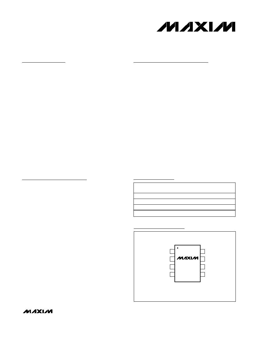
CNVST
REF
GND
1
2
8
7
SCLK
DOUT
AIN1 (AIN+)
AIN2 (AIN-)
V
DD
SOT23-8
TOP VIEW
( ) ARE FOR THE MAX1088/MAX1089
3
4
6
5
MAX1086
MAX1087
MAX1088
MAX1089
Pin Configuration
19-2036; Rev 0; 5/01
For pricing, delivery, and ordering information, please contact Maxim/Dallas Direct! at
1-888-629-4642, or visit Maxim's website at www.maxim-ic.com.
Ordering Information
AutoShutdown is a trademark of Maxim Integrated Products.
SPI and QSPI are trademarks of Motorola Inc.
MICROWIRE is a trademark of National Semiconductor Corp.
PART
TEMP.
RANGE
PIN-
PACKAGE
TOP
MARK
MAX1086EKA-T
-40°C to +85°C
8 SOT23
AAEZ
MAX1087EKA-T
-40°C to +85°C
8 SOT23
AAEV
MAX1088EKA-T
-40°C to +85°C
8 SOT23
AAFB
MAX1089EKA-T
-40°C to +85°C
8 SOT23
AAEX
MAX1086MAX1089
150ksps, 10-Bit, 2-Channel Single-Ended, and
1-Channel True-Differential ADCs in SOT23
2
_______________________________________________________________________________________
ABSOLUTE MAXIMUM RATINGS
ELECTRICAL CHARACTERISTICS
(V
DD
= +2.7V to +3.6V, V
REF
= +2.5V for MAX1087/MAX1089, or V
DD
= +4.75V to +5.25V, V
REF
= +4.096V for MAX1086/MAX1088,
0.1µF capacitor at REF, f
SCLK
= 8MHz (50% duty cycle), AIN- = GND for MAX1088/MAX1089. T
A
= T
MIN
to T
MAX,
unless otherwise
noted. Typical values at T
A
= +25°C.)
Stresses beyond those listed under "Absolute Maximum Ratings" may cause permanent damage to the device. These are stress ratings only, and functional
operation of the device at these or any other conditions beyond those indicated in the operational sections of the specifications is not implied. Exposure to
absolute maximum rating conditions for extended periods may affect device reliability.
V
DD
to GND .............................................................-0.3V to +6V
CNVST, SCLK, DOUT to GND......................-0.3V to (V
DD
+0.3V)
REF, AIN1(AIN+), AIN2(AIN-) to GND..........-0.3V to (V
DD
+0.3V)
Maximum Current Into Any Pin ...........................................50mA
Continuous Power Dissipation (T
A
= +70°C)
8-Pin SOT23(derate 9.70mW/°C above T
A
= +70°C) ....777mW
Operating Temperature Ranges.........................-40°C to +85°C
Storage Temperature Range .............................-60°C to +150°C
Lead Temperature (soldering, 10s) .................................+300°C
PARAMETER
SYMBOL
CONDITIONS
MIN
TYP
MAX
UNITS
DC ACCURACY (Note 1)
Resolution
10
Bits
Relative Accuracy (Note 2)
INL
±1.0
LSB
Differential Nonlinearity
DNL
No missing codes over temperature
±1.0
LSB
Offset Error
±0.5
±1.0
LSB
Gain Error (Note 3)
±1.0
±2.0
LSB
Gain Temperature Coefficient
±0.8
ppm/
°C
Channel-to-Channel Offset
±0.1
LSB
Channel-to-Channel Gain Matching
±0.1
LSB
Input Common-Mode Rejection
CMR
V
CM
= 0V to V
DD
; zero scale input
±0.1
mV
DYNAMIC SPECIFICATIONS: (f
IN
(sine-wave) = 10kHz, V
IN
= 4.096Vp-p for MAX1086/MAX1088 or V
IN
= 2.5V
PP
for MAX1087/MAX1089, 150ksps, f
SCLK
= 8MHZ, AIN- = GND for MAX1088/MAX1089)
Signal to Noise Plus Distortion
SINAD
61
dB
Total Harmonic Distortion
(up to the 5
th
harmonic)
THD
-70
dB
Spurious-Free Dynamic Range
SFDR
70
dB
Full-Power Bandwidth
-3dB point
1
MHz
Full-Linear Bandwidth
SINAD>56dB
100
kHz
CONVERSION RATE
Conversion Time
t
CONV
3.7
µs
T/H Acquisition Time
t
ACQ
1.4
µs
Aperture Delay
30
ns
Aperture Jitter
<50
ps
Maximum Serial Clock Frequency
f
SCLK
8
MHz
Duty Cycle
30
70
%
MAX1086MAX1089
150ksps, 10-Bit, 2-Channel Single-Ended, and
1-Channel True-Differential ADCs in SOT23
_______________________________________________________________________________________
3
ELECTRICAL CHARACTERISTICS (continued)
(V
DD
= +2.7V to +3.6V, V
REF
= +2.5V for MAX1087/MAX1089, or V
DD
= +4.75V to +5.25V, V
REF
= +4.096V for MAX1086/MAX1088,
0.1µF capacitor at REF, f
SCLK
= 8MHz (50% duty cycle), AIN- = GND for MAX1088/MAX1089. T
A
= T
MIN
to T
MAX,
unless otherwise
noted. Typical values at T
A
= +25°C.)
PARAMETER
SYMBOL
CONDITIONS
MIN
TYP
MAX
UNITS
ANALOG INPUT
Unipolar
0
V
REF
Input Voltage Range (Note 4)
Bipolar
-V
REF
/2
V
REF
/2
V
Input Leakage Current
C hannel not sel ected or conver si on stop p ed
±0.01
±1
µA
Input Capacitance
34
pF
EXTERNAL REFERENCE INPUT
Input Voltage Range
V
REF
1.0
V
DD
+50mV
V
V
REF
= +2.5V at 150ksps
16
30
V
REF
= +4.096V at 150ksps
26
45
Input Current
I
REF
Acquisition/Between conversions
±0.01
±1
µA
DIGITAL INPUTS/OUTPUT (SCLK, CNVST, DOUT)
Input Low Voltage
V
IL
0.8
V
Input High Voltage
V
IH
V
DD
-1
V
Input Leakage Current
I
L
±0.1
µA
Input Capacitance
C
IN
15
pF
I
SINK
= 2mA
0.4
V
Output Low Voltage
V
OL
I
SINK
= 4mA
0.8
V
Output High Voltage
V
OH
I
SOURCE
= 1.5mA
V
DD
-0.5
V
Three-State Leakage Current
I
L
CNVST = GND
±10
µA
Three-State Output Capacitance
C
OUT
CNVST = GND
15
pF
POWER REQUIREMENTS
MAX1086/MAX1088
4.75
5.0
5.25
Positive Supply Voltage
V
DD
MAX1087/MAX1089
2.7
3.0
3.6
V
f
SAMPLE
=150ksps
245
350
f
SAMPLE
=100ksps
150
f
SAMPLE
=10ksps
15
V
DD
= +3V
f
SAMPLE
=1ksps
2
f
SAMPLE
=150ksps
320
400
f
SAMPLE
=100ksps
215
f
SAMPLE
=10ksps
22
V
DD
= +5V
f
SAMPLE
=1ksps
2.5
Positive Supply Current
I
DD
Shutdown
0.2
5
µA
V
DD
= 5V
±5%; full-scale input
±0.1
1.0
Positive Supply Rejection
PSR
V
DD
= +2.7V to +3.6V; full-scale input
±0.1
±1.2
mV
MAX1086MAX1089
150ksps, 10-Bit, 2-Channel Single-Ended, and
1-Channel True-Differential ADCs in SOT23
4
_______________________________________________________________________________________
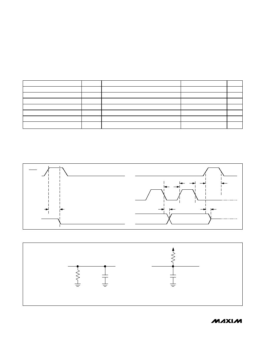
TIMING CHARACTERISTICS (Figures 1 and 2)
(V
DD
= +2.7V to +3.6V, V
REF
= +2.5V for MAX1087/MAX1089, or V
DD
= +4.75V to +5.25V, V
REF
= +4.096V for MAX1086/MAX1088,
0.1µF capacitor at REF, f
SCLK
= 8MHz (50% duty cycle); AIN- = GND for MAX1088/MAX1089. T
A
= T
MIN
to T
MAX,
unless otherwise
noted. Typical values at T
A
= +25°C.)
PARAMETERS
SYMBOL
CONDITIONS
MIN
TYP
MAX
UNITS
SCLK Pulse Width High
t
CH
38
ns
SCLK Pulse Width Low
t
CL
38
ns
SCLK Fall to DOUT Transition
t
DOT
C
LOAD
= 30pF
60
ns
SCLK Rise to DOUT Disable
t
DOD
C
LOAD
= 30pF
100
500
ns
CNVST Rise to DOUT Enable
t
DOE
C
LOAD
= 30pF
80
ns
CNVST Fall to MSB Valid
t
DOV
C
LOAD
= 30pF
3.7
µs
CNVST Pulse Width
t
CSW
30
ns
Note 1: Unipolar input.
Note 2: Relative accuracy is the deviation of the analog value at any code from its theoretical value after offset and gain errors have
been removed.
Note 3: Offset nulled.
Note 4: The absolute input range for the analog inputs is from GND to V
DD
.
· · ·
· · ·
· · ·
CNVST
SCLK
DOUT
t
DOE
HIGH-Z
HIGH-Z
t
CSW
t
DOT
t
CL
t
CH
t
DOD
DOUT
6k
6k
C
L
GND
DOUT
C
L
GND
V
DD
a) HIGH -Z TO V
OH
, V
OL
TO V
OH
, AND V
OH
TO HIGH -Z
a) HIGH -Z TO V
OL
, V
OH
TO V
OL
, AND V
OL
TO HIGH -Z
Figure 1. Detailed Serial-Interface Timing Sequence
Figure 2. Load Circuits for Enable/Disable Times
MAX1086MAX1089
150ksps, 10-Bit, 2-Channel Single-Ended, and
1-Channel True-Differential ADCs in SOT23
_______________________________________________________________________________________
5
-1.0
-0.6
-0.8
-0.4
-0.2
0
0.2
0.4
0.6
0.8
1.0
0
400
200
600
800
1000
1200
INTEGRAL NONLINEARITY
vs. OUTPUT CODE
MAX1086-9 toc01
OUTPUT CODE
INL (LSB)
MAX1087/MAX1089
0
400
200
600
800
1000
1200
INTEGRAL NONLINEARITY
vs. OUTPUT CODE
MAX1086-9 toc02
OUTPUT CODE
INL (LSB)
-1.0
-0.6
-0.8
-0.4
-0.2
0
0.2
0.4
0.6
0.8
1.0
MAX1086/MAX1088
DIFFERENTIAL NONLINEARITY
vs. OUTPUT CODE
MAX1086-9 toc03
OUTPUT CODE
DNL (LSB)
0
400
600
200
800
1000
1200
-1.0
-0.6
-0.8
-0.4
-0.2
0
0.2
0.4
0.6
0.8
1.0
MAX1087/MAX1089
DIFFERENTIAL NONLINEARITY
vs. OUTPUT CODE
MAX1086-9 toc04
OUTPUT CODE
0
400
600
200
800
1000
1200
DNL (LSB)
-1.0
-0.6
-0.8
-0.4
-0.2
0
0.2
0.4
0.6
0.8
1.0
MAX1086/MAX1088
1000
1
0.001
10
1000
SUPPLY CURRENT
vs. SAMPLING RATE
10
100
MAX1086-9 toc05
SAMPLING RATE (ksps)
SUPPLY CURRENT (
µ
A)
1.0
0.1
MAX1087/MAX1089
1000
1
SUPPLY CURRENT
vs. SAMPLING RATE
10
100
MAX1086-9 toc06
SAMPLING RATE (ksps)
SUPPLY CURRENT (
µ
A)
0.1
MAX1086/MAX1088
0.001
10
1000
1.0
180
280
230
330
380
2.7
3.7
3.2
4.2
4.7
5.2
SUPPLY CURRENT
vs. SUPPLY VOLTAGE
MAX1086-9 toc07
V
DD
(V)
SUPPLY CURRENT (
µ
A)
0
0.10
0.05
0.20
0.15
0.30
0.25
0.40
0.35
0.45
0.50
2.7
3.7
3.2
4.2
4.7
5.2
SHUTDOWN CURRENT
vs. SUPPLY VOLTAGE
MAX1086-9 toc08
V
DD
(V)
SHUTDOWN CURRENT (nA)
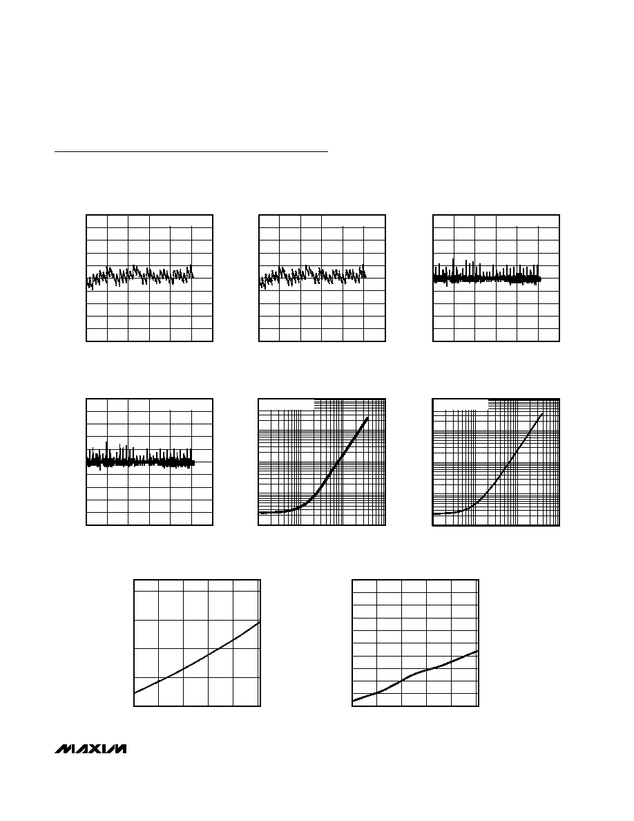
Typical Operating Characteristics
(V
DD
= +3.0V, V
REF
= +2.5V for MAX1087/MAX1089 or V
DD
= +5.0V, V
REF
= +4.096V for MAX1086/MAX1088, 0.1µF capacitor at
REF, f
SCLK
= 8MHz, (50% Duty Cycle), AIN- = GND for MAX1088/1089, T
A
= +25°C, unless otherwise noted.)