 | –≠–ª–µ–∫—Ç—Ä–æ–Ω–Ω—ã–π –∫–æ–º–ø–æ–Ω–µ–Ω—Ç: MAX108CHC | –°–∫–∞—á–∞—Ç—å:  PDF PDF  ZIP ZIP |

For the latest literature: http://www.maxim-ic.com, or phone 1-800-998-8800.
For small orders, phone 1-800-835-8769.
General Description
The MAX108 PECL-compatible, 1.5Gsps, 8-bit analog-
to-digital converter (ADC) allows accurate digitizing of
analog signals with bandwidths to 2.2GHz. Fabricated
on Maxim's proprietary advanced GST-2 bipolar
process, the MAX108 integrates a high-performance
track/hold (T/H) amplifier and a quantizer on a single
monolithic die.
The innovative design of the internal T/H, which has an
exceptionally wide 2.2GHz full-power input bandwidth,
results in high performance (typically 7.5 effective bits)
at the Nyquist frequency. A fully differential comparator
design and decoding circuitry reduce out-of-sequence
code errors (thermometer bubbles or sparkle codes)
and provide excellent metastable performance. Unlike
other ADCs that can have errors resulting in false full-
or zero-scale outputs, the MAX108 limits the error mag-
nitude to 1LSB.
The analog input is designed for either differential or
single-ended use with a ±250mV input voltage range.
Dual, differential, positive-referenced emitter-coupled
logic (PECL)-compatible output data paths ensure easy
interfacing and include an 8:16 demultiplexer feature
that reduces output data rates to one-half the sampling
clock rate. The PECL outputs can be operated from any
supply between +3V to +5V for compatibility with +3.3V
or +5V referenced systems. Control inputs are provided
for interleaving additional MAX108 devices to increase
the effective system sampling rate.
The MAX108 is packaged in a 25mm x 25mm, 192-con-
tact Enhanced Super Ball-Grid Array (ESBGATM) and is
specified over the commercial (0∞C to +70∞C) tempera-
ture range. For pin-compatible, lower speed versions of
the MAX108, see the MAX104 (1Gsps) and the MAX106
(600Msps) data sheets.
Applications
Digital RF/IF Signal Processing
Direct RF Downconversion
High-Speed Data Acquisition
Digital Oscilloscopes
High-Energy Physics
Radar/ECM Systems
ATE Systems
Features
o
1.5Gsps Conversion Rate
o
2.2GHz Full-Power Analog Input Bandwidth
o
7.5 Effective Bits at f
IN
= 750MHz (Nyquist
Frequency)
o
±0.25LSB INL and DNL
o
50
Differential Analog Inputs
o
±250mV Input Signal Range
o
On-Chip, +2.5V Precision Bandgap Voltage
Reference
o
Latched, Differential PECL Digital Outputs
o
Selectable 8:16 Demultiplexer
o
Internal Demux Reset Input with Reset Output
o
192-Contact ESBGA Package
o
Pin Compatible with MAX104 (1Gsps) and
MAX106 (600Msps)
MAX108
±5V, 1.5Gsps, 8-Bit ADC with
On-Chip 2.2GHz Track/Hold Amplifier
________________________________________________________________
Maxim Integrated Products
1
19-1492; Rev 0; 9/99
PART
MAX108CHC
0∞C to +70∞C
TEMP. RANGE
PIN-PACKAGE
192 ESBGA
EVALUATION KIT
AVAILABLE
Ordering Information
ESBGA
TOP VIEW
MAX108
Typical Operating Circuit appears at end of data sheet.
192-Contact ESBGA
Ball Assignment Matrix
ESBGA is a trademark of Amkor/Anam.
PCB land pattern appears at end of data sheet.
MAX108
±5V, 1.5Gsps, 8-Bit ADC with
On-Chip 2.2GHz Track/Hold Amplifier
2
_______________________________________________________________________________________
ABSOLUTE MAXIMUM RATINGS
Stresses beyond those listed under "Absolute Maximum Ratings" may cause permanent damage to the device. These are stress ratings only, and functional
operation of the device at these or any other conditions beyond those indicated in the operational sections of the specifications is not implied. Exposure to
absolute maximum rating conditions for extended periods may affect device reliability.
V
CC
A to GNDA .........................................................-0.3V to +6V
V
CC
D to GNDD.........................................................-0.3V to +6V
V
CC
I to GNDI ............................................................-0.3V to +6V
V
CC
O to GNDD ........................................-0.3V to (V
CC
D + 0.3V)
AUXEN1, AUXEN2 to GND .....................-0.3V to (V
CC
D + 0.3V)
V
EE
to GNDI..............................................................-6V to +0.3V
Between GNDs......................................................-0.3V to +0.3V
V
CC
A to V
CC
D .......................................................-0.3V to +0.3V
V
CC
A to V
CC
I .........................................................-0.3V to +0.3V
PECL Digital Output Current ...............................................50mA
REFIN to GNDR ........................................-0.3V to (V
CC
I + 0.3V)
REFOUT Current ................................................+100µA to -5mA
ICONST, IPTAT to GNDI .......................................-0.3V to +1.0V
TTL/CMOS Control Inputs
(DEMUXEN, DIVSELECT) ......................-0.3V to (V
CC
D + 0.3V)
RSTIN+, RSTIN- ......................................-0.3V to (V
CC
O + 0.3V)
VOSADJ Adjust Input ................................-0.3V to (V
CC
I + 0.3V)
CLK+ to CLK- Voltage Difference..........................................±3V
CLK+, CLK-.....................................(V
EE
- 0.3V) to (GNDD + 1V)
CLKCOM.........................................(V
EE
- 0.3V) to (GNDD + 1V)
VIN+ to VIN- Voltage Difference ............................................±2V
VIN+, VIN- to GNDI................................................................±2V
Continuous Power Dissipation (T
A
= +70∞C)
192-Contact ESBGA (derate 61mW/∞C above +70∞C) ....4.88W
(with heatsink and 200 LFM airflow,
derate 106mW/∞C above +70∞C) .....................................8.48W
Operating Temperature Range
MAX108CHC.........................................................0∞C to +70∞C
Operating Junction Temperature.....................................+150∞C
Storage Temperature Range .............................-65∞C to +150∞C
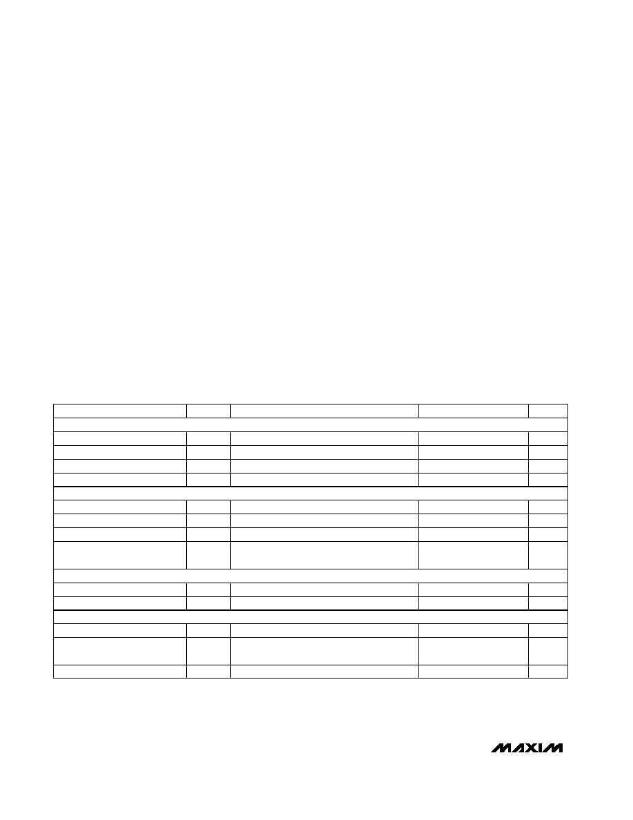
DC ELECTRICAL CHARACTERISTICS
(V
CC
A = V
CC
I = V
CC
D = +5.0V ±5%, V
EE
= -5.0V ±5%, V
CC
O = +3.0V to V
CC
D, REFIN connected to REFOUT, T
A
= T
MIN
to T
MAX
,
unless otherwise noted. Typical values are at T
A
= +25∞C.)
PARAMETER
SYMBOL
MIN
TYP
MAX
UNITS
Missing Codes
None
Codes
Differential Nonlinearity (Note 1)
DNL
-0.5
±0.25
0.5
LSB
Full-Scale Input Range
V
FSR
475
500
525
mVp-p
Common-Mode Input Range
V
CM
±0.8
V
Input Resistance
R
IN
49
50
51
Input Resistance Temperature
Coefficient
TC
R
150
ppm/∞C
Resolution
RES
8
Bits
Integral Nonlinearity (Note 1)
INL
-0.5
±0.25
0.5
LSB
Input Resistance (Note 2)
R
VOS
14
25
k
Input V
OS
Adjust Range
±4
±5.5
LSB
Reference Output Voltage
REFOUT
2.475
2.50
2.525
V
Reference Output Load
Regulation
REFOUT
5
mV
Reference Input Resistance
R
REF
4
5
k
CONDITIONS
No missing codes guaranteed
T
A
= +25∞C
Note 1
Signal + offset w.r.t. GNDI
VOSADJ = 0 to 2.5V
VIN+ and VIN- to GNDI, T
A
= +25∞C
Driving REFIN input only
0 < I
SOURCE
< 2.5mA
Referenced to GNDR
T
A
= +25∞C
ACCURACY
ANALOG INPUTS
VOS ADJUST CONTROL INPUT
REFERENCE INPUT AND OUTPUT
MAX108
±5V, 1.5Gsps, 8-Bit ADC with
On-Chip 2.2GHz Track/Hold Amplifier
_______________________________________________________________________________________
3
DC ELECTRICAL CHARACTERISTICS (continued)
(V
CC
A = V
CC
I = V
CC
D = +5.0V ±5%, V
EE
= -5.0V ±5%, V
CC
O = +3.0V to V
CC
D, REFIN connected to REFOUT, T
A
= T
MIN
to T
MAX
,
unless otherwise noted. Typical values are at T
A
= +25∞C.)
PECL DIGITAL OUTPUTS
(Note 5)
Negative Power-Supply
Rejection Ratio (Note 8)
PSRR-
40
68
dB
(Note 10)
Common-Mode Rejection Ratio
(Note 7)
CMRR
40
68
dB
Positive Power-Supply Rejection
Ratio (Note 8)
PSRR+
40
73
dB
VIN+ = VIN- = ±0.1V
(Note 9)
Positive Analog Supply Current
I
CC
A
480
780
mA
Positive Input Supply Current
I
CC
I
108
150
mA
Negative Input Supply Current
I
EE
-290
-210
mA
Digital Supply Current
I
CC
D
205
340
mA
Output Supply Current (Note 6)
I
CC
O
75
115
mA
Power Dissipation (Note 6)
P
DISS
5.25
W
Digital Output High Voltage
V
OH
-1.025
-0.880
V
Digital Output Low Voltage
V
OL
-1.810
-1.620
V
PARAMETER
SYMBOL
MIN
TYP
MAX
UNITS
High-Level Input Voltage
V
IH
2.0
V
Low-Level Input Voltage
V
IL
0.8
V
High-Level Input Current
I
IH
50
µA
Clock Input Resistance
R
CLK
48
50
52
Input Resistance Temperature
Coefficient
TC
R
150
ppm/∞C
Low-Level Input Current
I
IL
-1
1
µA
Digital Input High Voltage
V
IH
-1.165
V
Digital Input Low Voltage
V
IL
-1.475
V
CONDITIONS
V
IL
= 0
V
IH
= 2.4V
CLK+ and CLK- to CLKCOM, T
A
= +25∞C
CLOCK INPUTS
(Note 3)
TTL/CMOS CONTROL INPUTS (DEMUXEN, DIVSELECT)
DEMUX RESET INPUT
(Note 4)
POWER REQUIREMENTS
PECL DIGITAL OUTPUTS
(Note 5)
MAX108
±5V, 1.5Gsps, 8-Bit ADC with
On-Chip 2.2GHz Track/Hold Amplifier
4
_______________________________________________________________________________________
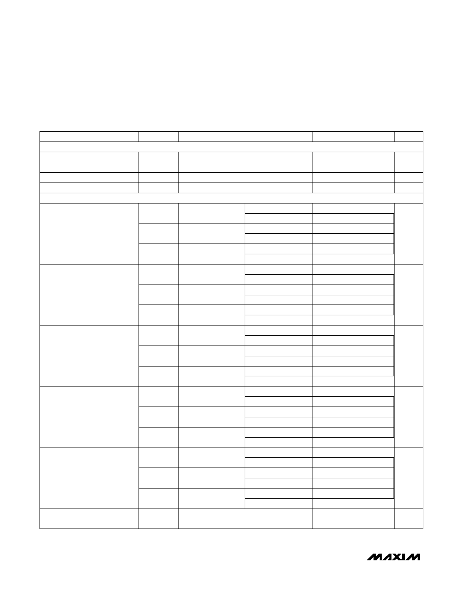
AC ELECTRICAL CHARACTERISTICS
(V
CC
A = V
CC
I = V
CC
D = +5.0V, V
EE
= -5.0V, V
CC
O = +3.3V, REFIN connected to REFOUT, f
S
= 1.5Gsps, f
IN
at -1dBFS, T
A
= +25∞C,
unless otherwise noted.)
Transfer Curve Offset
V
OS
-2.0
0
+2.0
LSB
VOSADJ control input open
Single-ended
Differential
45.7
48.2
Signal-to-Noise Ratio and
Distortion (Note 11)
SINAD
250
48.2
dB
f
IN
= 250MHz
Single-ended
Differential
44.5
47.0
Single-ended
Differential
SINAD
750
47.1
44.3
SINAD
1500
44.4
f
IN
= 1500MHz
f
IN
= 750MHz
Single-ended
Differential
55.0
61.6
Spurious-Free Dynamic Range
SFDR
250
61.7
dB
f
IN
= 250MHz
Single-ended
Differential
50.0
54.0
Single-ended
Differential
SFDR
750
54.1
44.6
SFDR
1500
45.5
f
IN
= 1500MHz
f
IN
= 750MHz
Single-ended
Differential
-55.5
-60.2
Total Harmonic Distortion
(Note 12)
THD
250
-61.3
dB
f
IN
= 250MHz
Single-ended
Differential
-49.0
-52.1
Single-ended
Differential
THD
750
-52.8
-44.5
THD
1500
-44.2
f
IN
= 1500MHz
f
IN
= 750MHz
Single-ended
Differential
44.2
47.4
Signal-to-Noise Ratio
(No Harmonics)
SNR
250
47.4
dB
f
IN
= 250MHz
Single-ended
Differential
43.3
46.8
SNR
750
46.9
f
IN
= 750MHz
Single-ended
Differential
7.3
7.71
Effective Number of Bits
(Note 11)
ENOB
250
7.71
Bits
Single-ended
Differential
f
IN
= 250MHz
44.8
SNR
1500
44.9
f
IN
= 1500MHz
Single-ended
Differential
7.1
7.51
ENOB
750
7.53
f
IN
= 750MHz
Single-ended
Differential
PARAMETER
SYMBOL
MIN
TYP
MAX
UNITS
7.07
Analog Input VSWR
VSWR
1.1:1
V/V
Analog Input Full-Power
Bandwidth
BW
-3dB
2.2
GHz
ENOB
1500
7.07
Two-Tone Intermodulation
IMD
-66.8
dB
CONDITIONS
f
IN
= 1500MHz
f
IN
= 500MHz
f
IN1
= 247MHz, f
IN2
= 253MHz,
at -7dB below full-scale
ANALOG INPUT
DYNAMIC SPECIFICATIONS
MAX108
±5V, 1.5Gsps, 8-Bit ADC with
On-Chip 2.2GHz Track/Hold Amplifier
_______________________________________________________________________________________
5
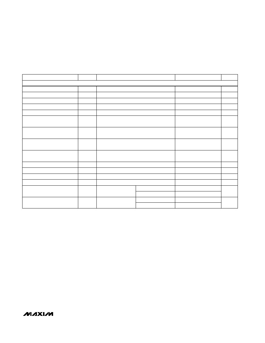
AC ELECTRICAL CHARACTERISTICS (continued)
(V
CC
A = V
CC
I = V
CC
D = +5.0V, V
EE
= -5.0V, V
CC
O = +3.3V, REFIN connected to REFOUT, f
S
= 1.5Gsps, f
IN
at -1dBFS, T
A
= +25∞C,
unless otherwise noted.)
DIV4 mode
DIV1, DIV2 modes
7.5
DIV4 mode
DIV1, DIV2 modes
Figures 6, 7, 8
t
PDP
Auxiliary Port Pipeline
Delay
t
PDA
9.5
Clock
Cycles
Figures 6, 7, 8
8.5
DREADY to DATA Propagation
Delay (Note 14)
t
PD2
-50
150
350
ps
Figure 17
CLK to DREADY Propagation
Delay
t
PD1
2.2
ns
Figure 17
Reset Input Data Hold Time
(Note 13)
t
HD
0
ps
Figure 15
Clock Pulse Width High
t
PWH
0.3
5
ns
Figure 17
PARAMETER
SYMBOL
MIN
TYP
MAX
UNITS
Aperture Jitter
t
AJ
<0.5
ps
Aperture Delay
t
AD
100
ps
Reset Input Data Setup Time
(Note 13)
t
SU
0
ps
DATA Rise Time
t
RDATA
420
ps
Maximum Sample Rate
f
MAX
1.5
Gsps
Clock Pulse Width Low
t
PWL
0.3
ns
DATA Fall Time
t
FDATA
360
ps
DREADY Rise Time
t
RDREADY
220
ps
DREADY Fall Time
t
FDREADY
180
ps
Primary Port Pipeline
Delay
7.5
Clock
Cycles
CONDITIONS
Figure 4
Figure 4
Figure 15
20% to 80%, C
L
= 3pF
20% to 80%, C
L
= 3pF
20% to 80%, C
L
= 3pF
20% to 80%, C
L
= 3pF
Figure 17
TIMING CHARACTERISTICS
Note 1:
Static linearity parameters are computed from a "best-fit" straight line through the code transition points. The full-scale
range (FSR) is defined as 256 times the slope of the line.
Note 2:
The offset control input is a self-biased voltage divider from the internal +2.5V reference voltage. The nominal open-circuit
voltage is +1.25V. It may be driven from an external potentiometer connected between REFOUT and GNDI.
Note 3:
The clock input's termination voltage can be operated between -2.0V and GNDI. Observe the absolute maximum ratings
on the CLK+ and CLK- inputs.
Note 4:
Input logic levels are measured with respect to the V
CC
O power-supply voltage.
Note 5:
All PECL digital outputs are loaded with 50
to V
CC
O - 2.0V. Measurements are made with respect to the V
CC
O power-
supply voltage.
Note 6:
The current in the V
CC
O power supply does not include the current in the digital output's emitter followers, which is a func-
tion of the load resistance and the V
TT
termination voltage.
Note 7:
Common-mode rejection ratio (CMRR) is defined as the ratio of the change in the transfer-curve offset voltage to the
change in the common-mode voltage, expressed in dB.
Note 8:
Power-supply rejection ratio (PSRR) is defined as the ratio of the change in the transfer-curve offset voltage to the change
in power-supply voltage, expressed in dB.
Note 9:
Measured with the positive supplies tied to the same potential; V
CC
A = V
CC
D = V
CC
I. V
CC
varies from +4.75V to +5.25V.
Note 10:
V
EE
varies from -5.25V to -4.75V.