Äîêóìåíòàöèÿ è îïèñàíèÿ www.docs.chipfind.ru
General Description
The MAX1098/MAX1099 implement both local and
remote temperature sensing with 10-bit resolution,
using +5V and +3V supply voltages, respectively.
Accuracy is ±1°C from 0°C to +70°C, with no calibra-
tion needed. The devices feature an algorithmic
switched-capacitor analog-to-digital converter (ADC),
on-chip clock, and 3-wire serial interface compatible
with SPITM, QSPITM, and MICROWIRETM.
The MAX1098/MAX1099 also perform fully differential
voltage measurements with 10-bit resolution and sepa-
rate track-and-hold (T/N) for positive and negative
inputs. Both devices accept versatile input modes con-
sisting of two 3-channel signal pairs, five 1-channel sig-
nals relative to a floating common, or V
DD
/4 relative to
ground. An external reference may be used for more
accurate voltage measurements.
Typical power consumption is only 1.3mW (MAX1099).
A shutdown mode and two standby modes provide
multiple strategies for prolonging battery life in portable
applications that require limited sampling throughput.
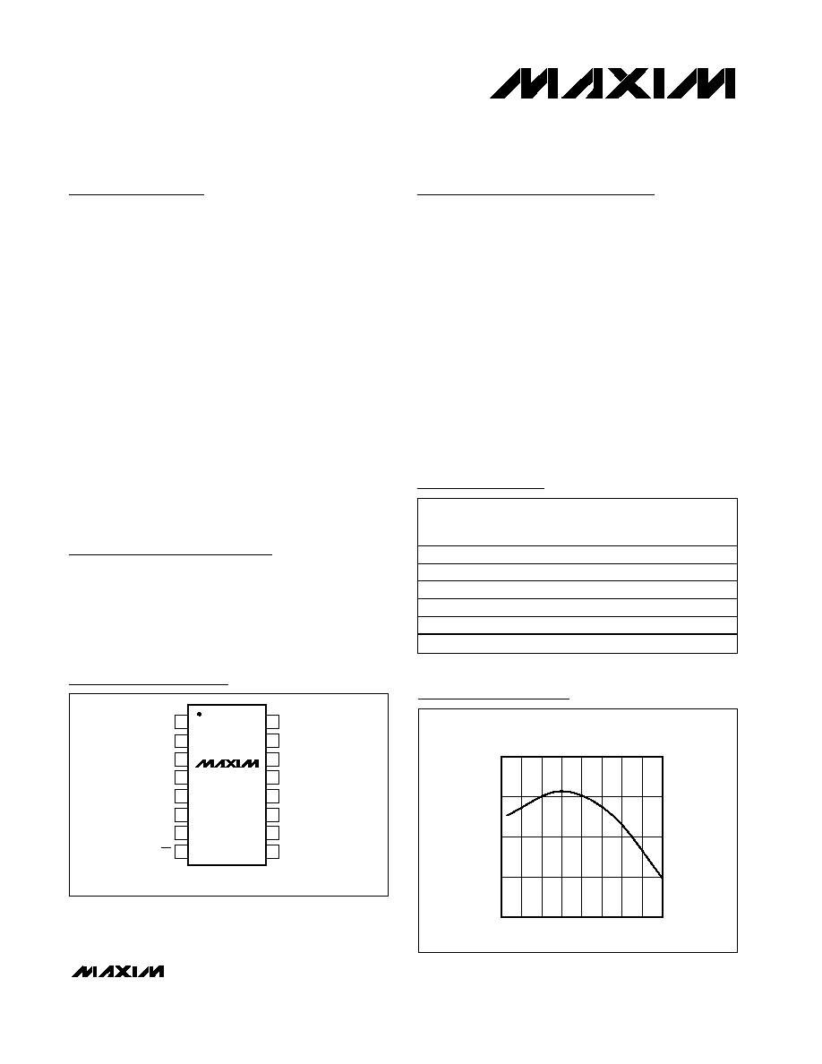
The MAX1098/MAX1099 are available in 16-pin SSOP
packages.
Applications
Temperature/Voltage Supervision of
Workstations and Communications Equipment
Hand-Held Instruments
Medical Equipment
Industrial Process Control
Features
o Local and Remote Temperature Sensing
o 12-Bit Resolution for Temperature and
10-Bit Resolution for Voltage Inputs
o ±1°C Accuracy from -40°C to +85°C
o Fully Differential Inputs
o Single-Supply Operation
+4.75V to +5.25V (MAX1098)
+2.7V to +3.6V (MAX1099)
o 3-Wire SPI/QSPI/MICROWIRE-Compatible
Interface
o Internal Precision Voltage Reference
2.50V (MAX1098)
1.20V (MAX1099)
o Space-Saving 16-Pin SSOP Package
MAX1098/MAX1099
10-Bit Serial-Output Temperature Sensors
with 5-Channel ADC
________________________________________________________________ Maxim Integrated Products
1
16
15
14
13
12
11
10
9
1
2
3
4
5
6
7
8
AIN1
AIN0
AIN5
REF
GND
V
DD
SCLK
DIN
COUT
TOP VIEW
MAX1098
MAX1099
SSOP
SHO
AIN2
GND
AIN3
AIN4
SSTRB
CS
Pin Configuration
19-1728; Rev 0; 7/00
For free samples and the latest literature, visit www.maxim-ic.com or phone 1-800-998-8800.
For small orders, phone 1-800-835-8769.
Ordering Information
*Future product--contact factory for availability.
Typical Operating Circuit appears at end of data sheet.
SPI and QSPI are trademarks of Motorola, Inc.
MICROWIRE is a trademark of National Semiconductor Corp.
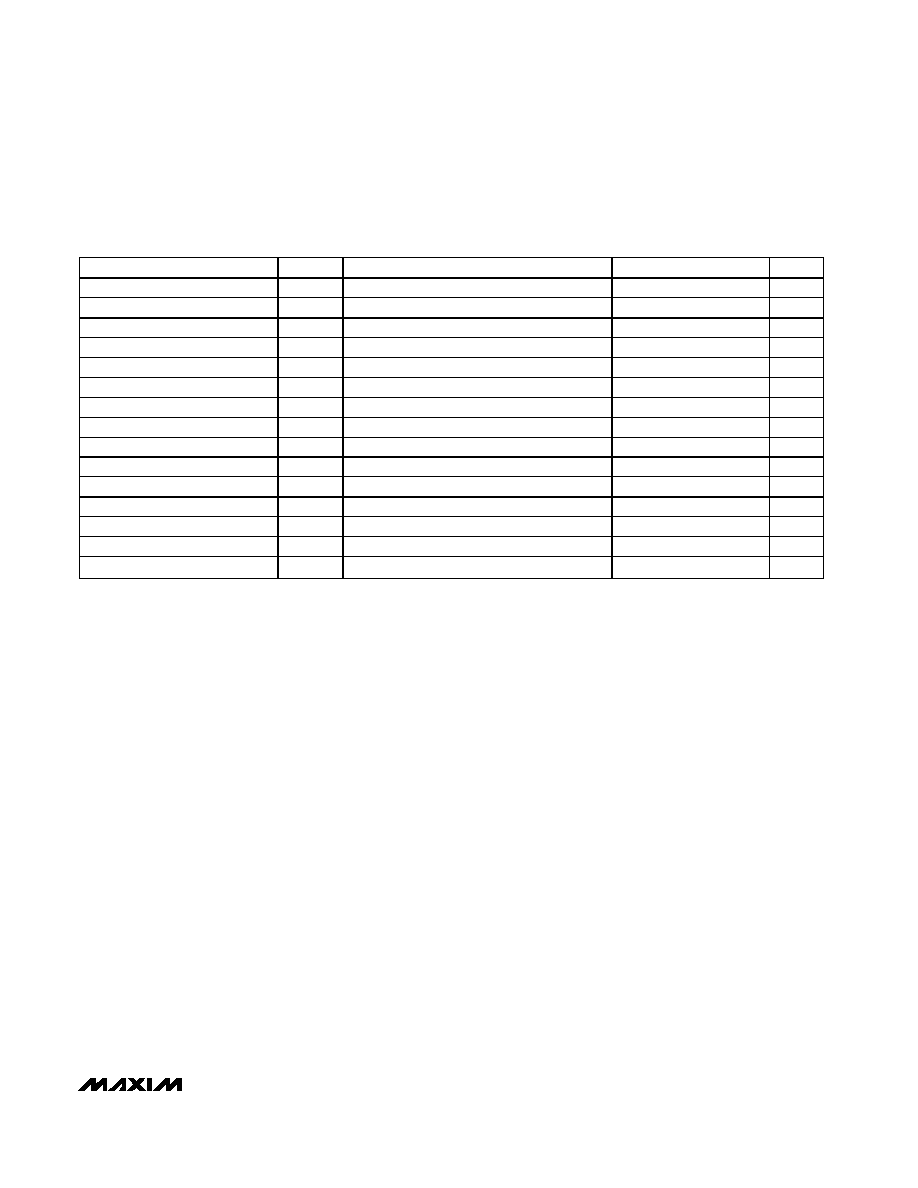
PART
TEMP.
RANGE
PIN-
PACKAGE
TEMP. SENSE
ACCURACY
(
°C)
MAX1098AEAE* -40
°C to +85°C 16 SSOP
±0.75
MAX1098BEAE* -40
°C to +85°C 16 SSOP
±1.0
MAX1098CEAE -40
°C to +85°C 16 SSOP
±4.0
MAX1099AEAE* -40
°C to +85°C 16 SSOP
±0.75
MAX1099BEAE* -40
°C to +85°C 16 SSOP
±1.0
MAX1099CEAE -40
°C to +85°C 16 SSOP
±4.0
-1.0
-0.5
0
0.5
1.0
-60
-20
20
60
-40
0
40
80
100
MAX1098
TEMPERATURE ERROR
vs. INTERNAL DIODE TEMPERATURE
MAX1098/9-29
TEMPERATURE (
°C)
TEMPERATURE ERROR (
°
C)
Temperature Error
MAX1098/MAX1099
10-Bit Serial-Output Temperature Sensors
with 5-Channel ADC
2
_______________________________________________________________________________________
ABSOLUTE MAXIMUM RATINGS
ELECTRICAL CHARACTERISTICS
(V
DD
= +4.75V to +5.25V (MAX1098), V
DD
= +2.7V to +3.6V (MAX1099), external reference, V
REF
= +2.5V (MAX1098), V
REF
= +1.2V
(MAX1099), f
SCLK
= 2.5MHz, T
A
= T
MIN
to T
MAX
, unless otherwise noted. Typical values are at T
A
= +25°C.)
Stresses beyond those listed under "Absolute Maximum Ratings" may cause permanent damage to the device. These are stress ratings only, and functional
operation of the device at these or any other conditions beyond those indicated in the operational sections of the specifications is not implied. Exposure to
absolute maximum rating conditions for extended periods may affect device reliability.
V
DD
to GND....................................................-0.3V to +6V
SHO to GND ................................................-0.3V to (V
DD
+0.3V)
Analog Inputs to GND
(AIN0AIN5, REF)...................................-0.3V to (V
DD
+0.3V)
Digital Inputs to GND (DIN, SCLK, CS).......-0.3V to (V
DD
+0.3V)
Digital Outputs to GND (DOUT, SSTRB) .....-0.3V to (V
DD
+0.3V)
Digital Output Sink Current .........................................25mA
Maximum Current into Any Pin.....................................50mA
Continuous Power Dissipation (T
A
= +70°C)
16-Pin SSOP (derate 8.00mW/°C above +70°C) ........667mW
Operating Temperature Range
MAX109_ _EAE ...............................................-40°C to +85°C
Junction Temperature..............................................+150°C
Storage Temperature Range .............................-65°C to +150°C
Lead Temperature (soldering, 10s) .................................+300°C
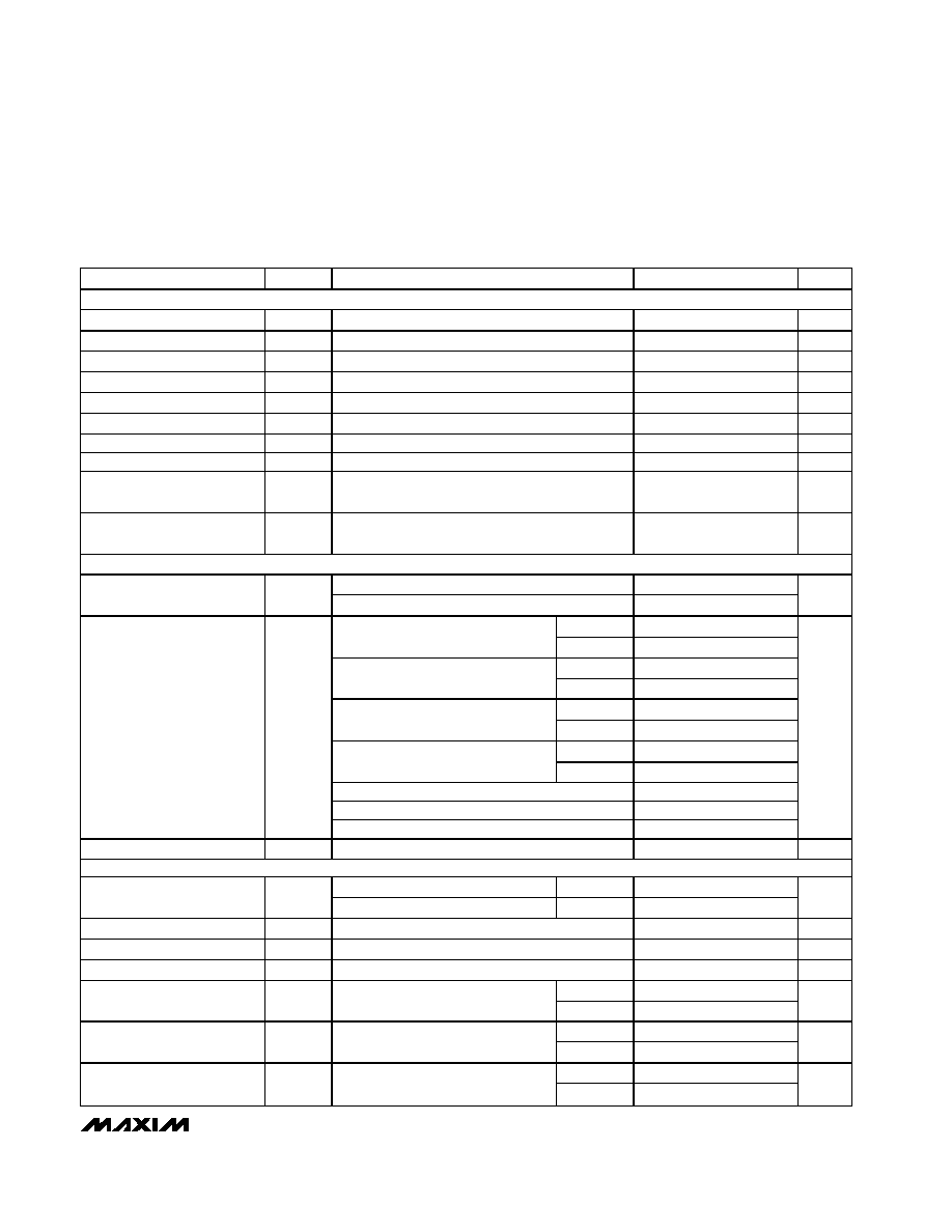
PARAMETER
SYMBOL
CONDITIONS
MIN
TYP
MAX
UNITS
DC ACCURACY (Note 1)
Resolution
RES
10
Bits
Relative Accuracy (Note 2)
INL
±1
LSB
Differential Nonlinearity
DNL
±1
LSB
Offset Error
Inputs AIN0
-AIN5
±1
LSB
Offset Temperature Coefficient
±10
µV/°C
Gain Error
Inputs AIN0
-AIN5, offset nulled
±1
LSB
V
DD
/4 Absolute Error
±1
LSB
Gain Temperature Coefficient
±2
ppm/
°C
Channel-to-Channel Offset
Matching
±0.25
LSB
CONVERSION RATE
Voltage measurement
1.1
Conversion Time (Note 3)
t
CONV
Temperature measurement
2.2
ms
Track/Hold Acquisition Time
t
ACQ
16
µs
Aperture Delay
t
APR
30
ns
Internal Clock Frequency
f
CLK
57.6
62.3
65.5
kHz
ANALOG INPUTS (AIN0
-AIN5)
Input Voltage Range (Note 4)
Measurement with respect to IN-, Figure 1
-2V
REF
+2V
REF
V
Common-Mode Range
0
V
DD
V
Input Current (Note 5)
0.1
5
µA
Input Capacitance
16
pF
MAX1098/MAX1099
10-Bit Serial-Output Temperature Sensors
with 5-Channel ADC
________________________________________________________________________________________
3
ELECTRICAL CHARACTERISTICS (continued)
(V
DD
= +4.75V to +5.25V (MAX1098), V
DD
= +2.7V to +3.6V (MAX1099), external reference, V
REF
= +2.5V (MAX1098), V
REF
= +1.2V
(MAX1099), f
SCLK
= 2.5MHz, T
A
= T
MIN
to T
MAX
, unless otherwise noted. Typical values are at T
A
= +25°C.)
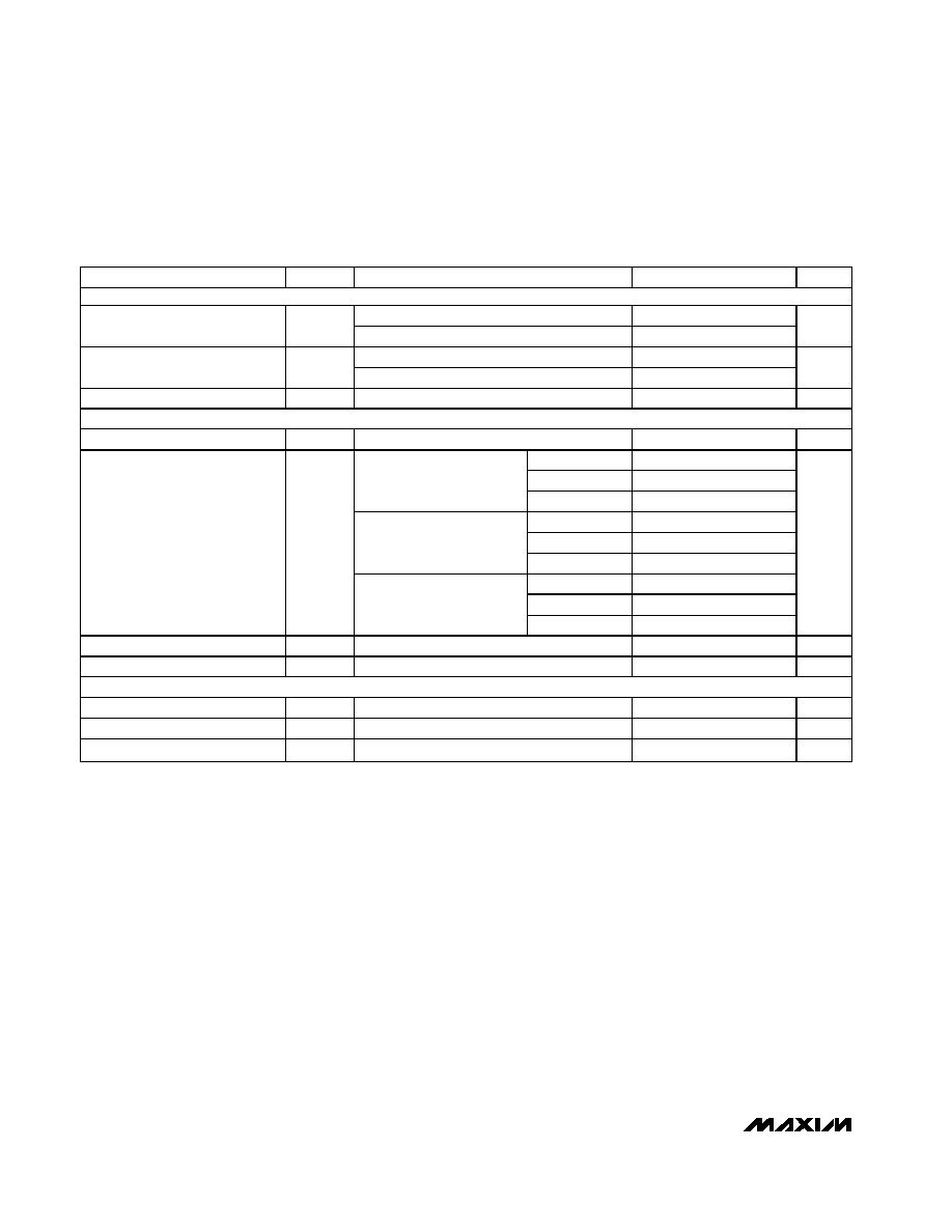
PARAMETER
SYMBOL
CONDITIONS
MIN
TYP
MAX
UNITS
DIGITAL INPUTS
Input Voltage Low
V
IL
0.8
V
Input Voltage High
V
IH
V
D D
- 0.8
V
Input Hysteresis
V
HYST
0.2
V
Input Leakage Current
I
IN
1
µA
Input Capacitance
16
pF
DIGITAL OUTPUTS
V
Output Low Voltage
V
OL
I
SINK
= 5mA
0.6
V
Output High Voltage
V
OH
I
SOURCE
= 0.5mA
V
D D
- 0.6
V
Three-State Output Leakage
Current
I
OUT
±10
µA
Three-State Output
Capacitance
15
pF
POWER REQUIREMENTS
MAX1098
4.75
5.25
Positive Supply Voltage
V
DD
MAX1099
2.7
3.6
V
MAX1098
390
Full-on, voltage measurements,
internal reference
MAX1099
350
MAX1098
310
Full-on, voltage measurements,
external reference
MAX1099
280
MAX1098
440
500
Ful l - on, tem p er atur e m easur em ents,
i nter nal r efer ence
MAX1099
400
500
MAX1098
360
Ful l - on, tem p er atur e m easur em ents,
exter nal r efer ence
MAX1099
330
Standby, SCLK = GND
120
Standby-plus, SCLK = GND
190
Positive Supply Current
(Note 6)
I
DD
Shutdown, SCLK = GND
2
10
µA
Power-Supply Rejection
PSRR
(Note 7)
50
65
dB
INTERNAL VOLTAGE REFERENCE CHARACTERISTICS
V
DD
= 5V
MAX1098
2.494
2.50
2.506
Reference Voltage
V
REF
V
DD
= 3V
MAX1099
1.197
1.20
1.203
V
Reference Tempco
TC V
REF
±20
ppm/
°C
Output Short-Circuit Current
1.25
mA
Capacitive Bypass at REF
0.1
µF
MAX1098
130
REF Output Noise
f
N
= 10Hz to 10kHz
MAX1099
65
µV
RMS
MAX1098
+3.0
REF Line Regulation
MAX1099
+0.2
mV/V
MAX1098
4
10
REF Load Regulation
0 to 100
µA output current
(Note 8)
MAX1099
2
10
µV/µA
MAX1098/MAX1099
10-Bit Serial-Output Temperature Sensors
with 5-Channel ADC
4
_______________________________________________________________________________________
PARAMETER
SYMBOL
CONDITIONS
MIN
TYP
MAX
UNITS
EXTERNAL VOLTAGE REFERENCE CHARACTERISTICS
MAX1098
0.8
2.5
Reference Voltage Range
V
REF
MAX1099
0.8
1.2
V
Converting
10
REF Input Resistance
Shutdown
25
M
REF Input Capacitance
24
pF
INTERNAL TEMPERATURE MEASUREMENT CHARACTERISTICS
Resolution
0.13
°C
MAX109_A
±0.75
MAX109_B
±1
T
A
= +85
°C, P
D
= 1mW
MAX109_C
±1
MAX109_A
±0.75
MAX109_B
±1
T
A
= 0
°C to +70°C
MAX109_C
±2
MAX109_A
±0.75
MAX109_B
±1
Output Error (Notes 1, 9)
T
A
= -40
°C to 0°C,
T
A
= +70
°C to +85°C
MAX109_C
±4
°C
Power-Supply Rejection Ratio
PSRR
(Note 7)
0.2
°C/V
Noise
0.18
°C
RMS
EXTERNAL TEMPERATURE MEASUREMENT CHARACTERISTICS
Output Error
2N3904 (Note 10)
±2
±4
°C
Remote Diode Excitation (1X)
10
µA
Remote Diode Excitation (10X)
100
µA
ELECTRICAL CHARACTERISTICS (continued)
(V
DD
= 4.75V to 5.25V (MAX1098), V
DD
= 2.7V to 3.6V (MAX1099), external reference, V
REF
= +2.5V (MAX1098), V
REF
= +1.2V
(MAX1099), f
SCLK
= 2.5MHz, T
A
= T
MIN
to T
MAX
, unless otherwise noted. Typical values are at T
A
= +25°C.)
MAX1098/MAX1099
10-Bit Serial-Output Temperature Sensors
with 5-Channel ADC
________________________________________________________________________________________
5
TIMING CHARACTERISTICS
(V
DD
= +4.75V to +5.25V (MAX1098), V
DD
= +2.7V to +3.6V (MAX1099), external reference, V
REF
= +2.5V (MAX1098), V
REF
= +1.2V
(MAX1099), f
SCLK
= 2.5MHz, T
A
= T
MIN
to T
MAX
, unless otherwise noted. Typical values are at T
A
= +25°C.) (Figures 4, 6)
PARAMETER
SYMBOL
CONDITIONS
MIN
TYP
MAX
UNITS
SCLK Frequency
f
SCLK
2.5
MHz
SCLK Pulse Width Low
t
CL
200
ns
SCLK Pulse Width High
t
CH
200
ns
CS Low to SCLK High
t
CSS
100
ns
SCLK High to CS Setup
t
CSH
100
ns
CS Pulse Width
t
CS
100
ns
SCLK High to CS Low Setup
t
CS0
50
ns
SCLK High to CS High Setup
t
CS1
100
ns
DIN Setup to SCLK High Time
t
DS
100
ns
DIN Hold Time
t
DH
0
ns
SCLK Fall to Output Data Valid
t
DO
R
L
= 100k
, C
L
= 50pF
150
ns
CS Fall to Output Enable
t
DV
R
L
= 100k
, C
L
= 50pF
150
ns
CS Rise to Output Disable
t
TR
R
L
= 100k
, C
L
= 50pF
50
ns
SSTRB Rise to SCLK Rise
t
SCLK
0
ns
SCLK Fall to SSTRB Fall
t
SSTRB
200
ns
Note 1: Tested at V
DD
= +5.0V (MAX1098) and V
DD
= +3.0V (MAX1099).
Note 2: Relative accuracy is the deviation of the analog value at any code from its theoretical value after the full-scale range has
been calibrated.
Note 3: Conversion time is defined as the number of clock cycles (64 for voltage measurements, 125 for temperature measure-
ments) multiplied by the internal clock period.
Note 4: Individual analog input voltages cannot extend beyond the power-supply rails.
Note 5: Input resistance is typically 250M
; 5µA limit reflects limitations in production testing.
Note 6: Specifications for full-on status assume continuous conversions. Power modes are software selected (Table 3).
Note 7: Measured at V
FS(+4.75V)
- V
FS(+5.25V)
for the MAX1098 and at V
FS(+2.7V)
- V
FS(+3.6V)
for the MAX1099.
Note 8: External load should not change during conversions for specified accuracy.
Note 9: Excludes noise and self-heating effects. Output error for MAX109_C guaranteed by design.
Note 10: External temperature sensing over -40°C to +85°C range, device at +25°C. Guaranteed by design.