 | –≠–ª–µ–∫—Ç—Ä–æ–Ω–Ω—ã–π –∫–æ–º–ø–æ–Ω–µ–Ω—Ç: MAX110 | –°–∫–∞—á–∞—Ç—å:  PDF PDF  ZIP ZIP |
MAX110/MAX111
Low-Cost, 2-Channel, ±14-Bit Serial ADCs
________________________________________________________________
Maxim Integrated Products
1
General Description
The MAX110/MAX111 analog-to-digital converters
(ADCs) use an internal auto-calibration technique to
achieve 14-bit resolution plus overrange, with no exter-
nal components. Operating supply current is only
550µA (MAX110) and reduces to 4µA in power-down
mode, making these ADCs ideal for high-resolution bat-
tery-powered or remote-sensing applications. A fast
serial interface simplifies signal routing and opto-isola-
tion, saves microcontroller pins, and offers compatibility
with SPITM, QSPITM, and MICROWIRETM. The MAX110
operates with ±5V supplies, and converts differential
analog signals in the -3V to +3V range. The MAX111
operates with a single +5V supply and converts differ-
ential analog signals in the ±1.5V range, or single-
ended signals in the 0V to +1.5V range.
Internal calibration allows for both offset and gain-error
correction under microprocessor (µP) control. Both
devices are available in space-saving 16-pin DIP and
SO packages, as well as an even smaller 20-pin SSOP
package.
________________________Applications
Process Control
Weigh Scales
Panel Meters
Data-Acquisition Systems
Temperature Measurement
____________________________Features
o
Single +5V Supply (MAX111)
o
Two Differential Input Channels
o
14-Bit Resolution Plus Sign and Overrange
o
0.03% Linearity (MAX110)
0.05% Linearity (MAX111)
o
Low Power Consumption:
550µA (MAX110)
640µA (MAX111)
4µA Shutdown Current
o
Up to 50 Conversions/sec
o
50Hz/60Hz Rejection
o
Auto-Calibration Mode
o
No External Components Required
o
16-Pin DIP/SO, 20-Pin SSOP
Ordering Information
19-0283; Rev 5; 11/98
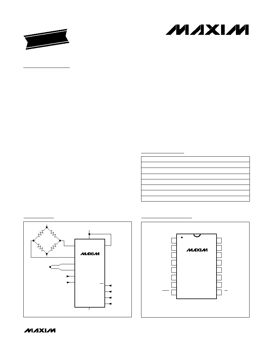
Typical Operating Circuit
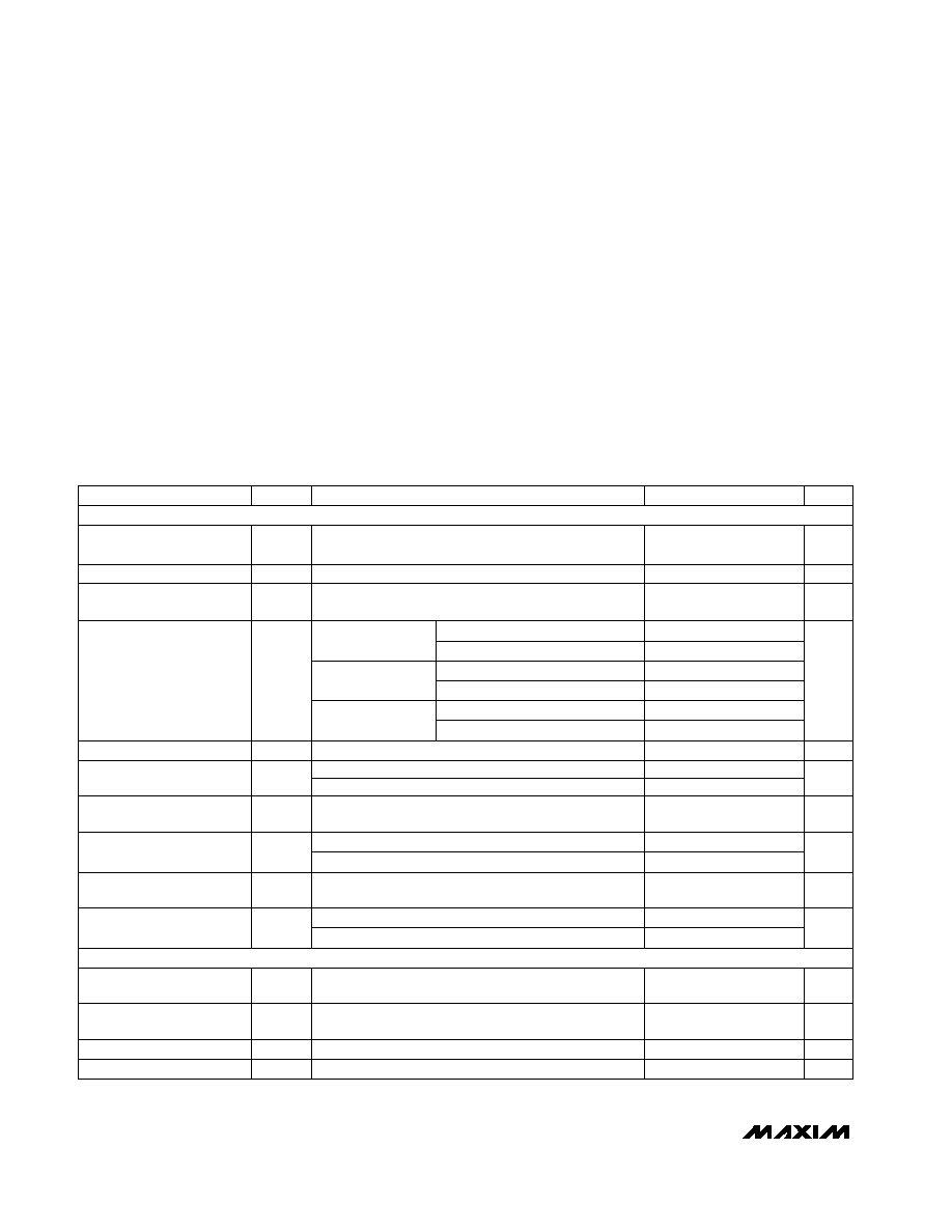
Pin Configurations
IN1+
IN1-
REF+
REF-
CS
RCSEL
SCLK
DIN
DOUT
IN2+
IN2-
V
DD
+5V
-5V (0V)
FROM
µ
C
MAX110
MAX111
( ) ARE FOR MAX111
V
SS
(AGND)
1
2
3
4
5
6
7
8
16
15
14
13
12
11
10
9
IN1+
REF-
REF+
V
DD
RCSEL
XCLK
SCLK
BUSY
IN1-
IN2+
IN2-
V
SS
(AGND)
GND
DIN
DOUT
CS
TOP VIEW
MAX110
MAX111
DIP/SO
( ) ARE FOR MAX111
PART
MAX110
ACPE
MAX110BCPE
MAX110ACWE
0∞C to +70∞C
0∞C to +70∞C
0∞C to +70∞C
TEMP. RANGE
PIN-PACKAGE
16 Plastic DIP
16 Plastic DIP
16 Wide SO
MAX110BCWE
0∞C to +70∞C
16 Wide SO
MAX110ACAP
0∞C to +70∞C
20 SSOP
MAX110BCAP
0∞C to +70∞C
20 SSOP
EVALUATION KIT
AVAILABLE
MAX110BC/D
0∞C to +70∞C
Dice*
Ordering Information continued at end of data sheet.
*
Contact factory for dice specifications.
SPI and QSPI are trademarks of Motorola, Inc. MICROWIRE is a trademark of National Semiconductor Corp.
Pin Configurations continued at end of data sheet.
INL(%)
±0.03
±0.05
±0.03
±0.05
±0.03
±0.05
±0.05
For free samples & the latest literature: http://www.maxim-ic.com, or phone 1-800-998-8800.
For small orders, phone 1-800-835-8769.
MAX110/MAX111
Low-Cost, 2-Channel, ±14-Bit Serial ADCs
2
_______________________________________________________________________________________
ABSOLUTE MAXIMUM RATINGS
V
DD
to GND ...........................................................................+6V
V
SS
to GND (MAX110)..............................................+0.3V to -6V
AGND to DGND.....................................................-0.3V to +0.3V
V
IN1+
, V
IN1-
......................................(V
DD
+ 0.3V) to (V
SS
- 0.3V)
V
IN2+
, V
IN2-
......................................(V
DD
+ 0.3V) to (V
SS
- 0.3V)
V
REF+
, V
REF-
....................................(V
DD
+ 0.3V) to (V
SS
- 0.3V)
Digital Inputs and Outputs .........................(V
DD
+ 0.3V) to -0.3V
Continuous Power Dissipation
16-Pin Plastic DIP (derate 10.53mW/∞C above +70∞C).....842mW
16-Pin Wide SO (derate 9.52mW/∞C above +70∞C) ......762mW
20-Pin SSOP (derate 8.00mW/∞C above +70∞C) ...........640mW
16-Pin CERDIP (derate 10.00mW/∞C above +70∞C)......800mW
Operating Temperature Ranges
MAX11_ _C_ _......................................................0∞C to +70∞C
MAX11_ _E_ _ ...................................................-40∞C to +85∞C
MAX11_BMJE .................................................-55∞C to +125∞C
Storage Temperature Range .............................-65∞C to +160∞C
Lead Temperature (soldering, 10sec) .............................+300∞C
Stresses beyond those listed under "Absolute Maximum Ratings" may cause permanent damage to the device. These are stress ratings only, and functional
operation of the device at these or any other conditions beyond those indicated in the operational sections of the specifications is not implied. Exposure to
absolute maximum rating conditions for extended periods may affect device reliability.
ELECTRICAL CHARACTERISTICS--MAX110
(V
DD
= 5V ±5%, V
SS
= -5V ±5%, f
XCLK
= 1MHz,
˜
2 mode (DV2 = 1), 81,920 CLK cycles/conv, V
REF+
= 1.5V, V
REF-
= -1.5V,
T
A
= T
MIN
to T
MAX
, unless otherwise noted. Typical values are at T
A
= +25∞C.)
LSB
nA
500
CONDITIONS
I
IN+
, I
IN-
Input Bias Current
(Note 3)
pF
10
-0.83 x V
REF
V
IN
0.83 x V
REF
-V
REF
V
IN
V
REF
-0.83 x V
REF
V
IN
0.83 x V
REF
Input Capacitance
-V
REF
V
IN
V
REF
V
V
SS
+
V
DD
-
2.25
2.25
V
IN+
,
V
IN-
Absolute Input Voltage
Range
V
-V
REF
+V
REF
V
IN
Differential Input Voltage
Range
ppm
30
Power-Supply Rejection
15
ppm/∞C
8
Full-Scale Error
Temperature Drift
%
±0.1
µV/∞C
0.003
Offset Error
Temperature Drift
(Note 6)
UNITS
MIN
TYP
MAX
SYMBOL
PARAMETER
mV
±4
Offset Error
±0.018
±0.03
±0.06
±0.015
±0.03
±0.04
V
IN+
= V
IN-
= 0V
MAX110BC/E
MAX110AC/E
After gain calibration (Note 5)
After offset null
V
SS
= -5V, V
DD
= 4.75V to 5.25V
V
DD
= 5V, V
SS
= -4.75V to -5.25V
(Notes 3, 4)
±2
DNL
Differential Nonlinearity
ppm/V
6
CMRR
Common-Mode Rejection
Ratio
-2.5V
(V
IN+
= V
IN-
)
2.5V
Uncalibrated
-8
0
Full-Scale Error
Uncalibrated
0.02
-V
REF
V
IN
V
REF
-0.83 x V
REF
V
IN
0.83 x V
REF
%FSR
INL
Relative Accuracy
(Notes 3, 5≠7)
±0.1
±0.05
MAX110BM
(Note 2)
14 + POL
+ OFL
RES
Resolution
Bits
No-Missing-Codes
Resolution
(Note 3)
13 + POL
+ OFL
Bits
ACCURACY
(Note 1)
ANALOG INPUTS

MAX110/MAX111
Low-Cost, 2-Channel, ±14-Bit Serial ADCs
_______________________________________________________________________________________
3
ELECTRICAL CHARACTERISTICS--MAX110 (continued)
(V
DD
= 5V ±5%, V
SS
= -5V ±5%, f
XCLK
= 1MHz,
˜
2 mode (DV2 = 1), 81,920 CLK cycles/conv, V
REF+
= 1.5V, V
REF-
= -1.5V,
T
A
= T
MIN
to T
MAX
, unless otherwise noted. Typical values are at T
A
= +25∞C.)
V
V
4.75
5.25
V
DD
Positive Supply Voltage
0.8
V
IL
V
-4.75
-5.25
V
SS
Negative Supply Voltage
µA
Input Low Voltage
550
950
780
I
DD
Positive Supply Current
V
DD
= 5.25V,
V
SS
= -5.25V
320
650
Performance guaranteed by supply rejection test
Performance guaranteed by supply rejection test
pF
10
0.4
V
DD
- 0.5
V
OH
Output High Voltage
Input Capacitance
f
XCLK
= 500kHz,
continuous-conversion mode
µA
µA
I
SS
Negative Supply Current
V
DD
= 5.25V,
V
SS
= -5.25V
±1
20.48
4
10
I
DD
I
LKG
Input Leakage Current
XCLK unloaded,
continuous-conversion mode, RC
oscillator operational (Note 9)
f
XCLK
= 500kHz,
continuous-conversion mode
(Note 3)
µA
±10
I
LKG
Leakage Current
pF
10
Output Capacitance
µA
0.05
2
Digital inputs at 0V or 5V
Power-Down Current
DOUT, BUSY, V
DD
= 4.75V, I
SOURCE
= 1.0mA
V
DD
= 5.25V, V
SS
= -5.25V, V
XCLK
= 0V, PD = 1
V
OUT
= 5V or 0V
(Note 3)
10,240 clock-cycles/conversion
DOUT, BUSY, I
SINK
= 1.6mA
CONDITIONS
UNITS
MIN
TYP
MAX
SYMBOL
PARAMETER
ms
204.80
t
CONV
Synchronous Conversion
Time (Note 7)
102,400 clock-cycles/conversion
MHz
0.25
1.25
f
OSC
Oversampling Clock
Frequency
(Note 8)
V
2.4
V
IH
Input High Voltage
I
SS
V
0
3.0
V
REF
Differential Reference
Input Voltage Range
pF
10
Reference Input
Capacitance
(Note 3)
V
0.4
V
OL
Output Low Voltage
XCLK, I
SINK
= 200µA
V
V
DD
- 0.5
XCLK, V
DD
= 4.75V, I
SOURCE
= 200µA
nA
500
I
REF+
,
I
REF-
Reference Input Current
V
REF+
= 2.5V, V
REF-
= 0V
V
V
SS
+
V
DD
-
2.25
2.25
V
REF+
,
V
REF-
Absolute Reference Input
Voltage Range
CONVERSION TIME
DIGITAL OUTPUTS
(DOUT, BUSY, and XCLK when RCSEL = V
DD
)
POWER REQUIREMENTS
(all digital inputs at 0V or 5V)
REFERENCE INPUTS
DIGITAL INPUTS
(CS, SCLK, DIN, and XCLK when RCSEL = 0V)

MAX110/MAX111
Low-Cost, 2-Channel, ±14-Bit Serial ADCs
4
_______________________________________________________________________________________
ELECTRICAL CHARACTERISTICS--MAX111
(V
DD
= 5V ±5%, f
XCLK
= 1MHz, ˜ 2 mode (DV2 = 1), 81,920 CLK cycles/conv, V
REF+
= 1.5V, V
REF-
= 0V, T
A
= T
MIN
to T
MAX
,
unless otherwise noted. Typical values are at T
A
= +25∞C.)
LSB
nA
500
CONDITIONS
I
IN+
, I
IN-
Input Bias Current
(Note 3)
pF
10
-0.667 x V
REF
V
IN
0.667 x V
REF
-V
REF
V
IN
V
REF
-0.667 x V
REF
V
IN
0.667 x V
REF
Input Capacitance
-V
REF
V
IN
V
REF
V
0
V
DD
- 3.2
V
IN+
,
V
IN-
Absolute Input Voltage
Range
V
-V
REF
+V
REF
V
IN
Differential Input Voltage
Range
-V
REF
V
IN
V
REF
ppm
15
V
DD
= 4.75V to 5.25V
Power-Supply Rejection
%FSR
INL
ppm/∞C
8
Full-Scale Error
Temperature Drift
Relative Accuracy,
Differential Input
(Notes 3, 5≠7)
(Notes 3, 4)
±0.25
±2
%
±0.2
±0.20
DNL
Differential Nonlinearity
(Note 6)
UNITS
MIN
TYP
MAX
SYMBOL
ppm/V
6
(Note 2)
PARAMETER
14 + POL
+ OFL
RES
Resolution
CMRR
mV
±4
Offset Error
Common-Mode Rejection
Ratio
10mV
(V
IN+
= V
IN-
)
2.0V
Bits
No-Missing-Codes
Resolution
±0.10
(Note 3)
-8
0
±0.05
±0.10
Full-Scale Error
Uncalibrated
±0.03
±0.05
MAX111BM
13 + POL
+ OFL
Bits
±0.18
V
IN+
= V
IN-
= 0V
MAX111BC/E
MAX111AC/E
After gain calibration (Note 5)
V
IN
0.667 x V
REF
0V
V
IN
V
REF
V
IN
0.667 x V
REF
0V
V
IN
V
REF
0V
V
IN
V
REF
V
IN
0.667 x V
REF
%FSR
INL
Relative Accuracy,
Single-Ended Input
(IN- = GND)
±0.25
±0.15
±0.10
±0.1
±0.06
MAX111BM
±0.18
MAX111BC/E
MAX111AC/E
ACCURACY (Note 1)
ANALOG INPUTS
-0.667 x V
REF
V
IN
0.667 x V
REF

MAX110/MAX111
Low-Cost, 2-Channel, ±14-Bit Serial ADCs
_______________________________________________________________________________________
5
ELECTRICAL CHARACTERISTICS--MAX111 (continued)
(V
DD
= 5V ±5%, f
XCLK
= 1MHz, ˜ 2 mode (DV2 = 1), 81,920 CLK cycles/conv, V
REF+
= 1.5V, V
REF-
= 0V, T
A
= T
MIN
to T
MAX
,
unless otherwise noted. Typical values are at T
A
= +25∞C.)
V
V
V
4.75
5.25
V
DD
Positive Supply Voltage
0.4
ms
V
OL
0.8
V
IL
204.80
Output Low Voltage
µA
Input Low Voltage
640
1200
t
CONV
Synchronous Conversion
Time (Note 7)
102,400 clock-cycles/conversion
XCLK, I
SINK
= 200µA
pF
10
Reference Input
Capacitance
MHz
0.25
1.25
nA
f
OSC
Oversampling Clock
Frequency
(Note 8)
V
2.4
V
IH
Input High Voltage
(Note 3)
V
0
1.5
V
REF
960
I
DD
Supply Current
V
DD
= 5.25V
Differential Reference
Input Voltage Range
Performance guaranteed by supply rejection test
500
I
REF+
,
I
REF-
Reference Input Current
pF
10
V
REF+
= 1.5V, V
REF-
= 0V
0.4
V
0
V
DD
- 3.2
V
REF+
,
V
REF-
V
DD
- 0.5
V
OH
Output High Voltage
Input Capacitance
Absolute Reference Input
Voltage Range
V
V
DD
- 0.5
f
XCLK
= 500kHz,
continuous-conversion mode
µA
±1
XCLK, V
DD
= 4.75V, I
SOURCE
= 200µA
20.48
4
10
I
DD
I
LKG
Input Leakage Current
XCLK unloaded,
continuous-conversion mode, RC
oscillator operational (Note 9)
(Note 3)
µA
±1
I
LKG
Leakage Current
pF
10
Output Capacitance
µA
Digital inputs at 0V or 5V
Power-Down Current
DOUT, BUSY, V
DD
= 4.75V, I
SOURCE
= 1.0mA
V
DD
= 5.25V, V
XCLK
= 0V, PD = 1
V
OUT
= 5V or 0V
(Note 3)
10,240 clock-cycles/conversion
DOUT, BUSY, I
SINK
= 1.6mA
CONDITIONS
UNITS
MIN
TYP
MAX
SYMBOL
PARAMETER
CONVERSION TIME
DIGITAL OUTPUTS
(DOUT, BUSY, and XCLK when RCSEL = V
DD
)
POWER REQUIREMENTS
(all digital inputs at 0V or 5V)
REFERENCE INPUTS
DIGITAL INPUTS
(CS, SCLK, DIN, and XCLK when RCSEL = 0V)