 | ÐлекÑÑоннÑй компоненÑ: MAX11015 | СкаÑаÑÑ:  PDF PDF  ZIP ZIP |
MAX11014 DS
General Description
The MAX11014/MAX11015 set and control bias condi-
tions for dual MESFET power devices found in point-to-
point communication and other microwave base
stations. The MAX11014 integrates complete dual ana-
log closed-loop drain-current controllers for Class A
MESFET amplifier operation, while the MAX11015 tar-
gets Class AB operation. Both devices integrate SRAM
lookup tables (LUTs) that can be used to store temper-
ature and drain-current compensation data.
Each device includes dual high-side current-sense
amplifiers to monitor the MESFET drain currents through
the voltage drop across the sense resistors in the 0 to
625mV range. External diode-connected transistors mon-
itor the MESFET temperatures while an internal tempera-
ture sensor measures the local die temperature of the
MAX11014/MAX11015. The internal DAC sets the volt-
ages across the current-sense resistors by controlling
the GATE voltages. The internal 12-bit SAR ADC digitizes
internal and external temperature, internal DAC voltages,
current-sense amplifier voltages, and external GATE volt-
ages. Two of the 11 ADC channels are available as gen-
eral-purpose analog inputs for analog system monitoring.
The MAX11014's gate-drive amplifier functions as an
integrator for the Class A drain-current control loop
while the MAX11015's gate-drive amplifier functions
with a gain of -2 for Class AB applications. The current-
limited gate-drive amplifier can be fast clamped to an
external voltage independent of the digital input from
the serial interface. Both the MAX11014 and the
MAX11015 include self-calibration modes to minimize
error over time, temperature, and supply voltage.
The MAX11014/MAX11015 feature an internal reference
and can operate from separate ADC and DAC external
references. The internal reference provides a well-regu-
lated, low-noise +2.5V reference for the ADC, DAC, and
temperature sensors. These integrated circuits operate
from a 4-wire 20MHz SPITM-/MICROWIRETM-compatible
or 3.4MHz I
2
C*-compatible serial interface (pin-selec-
table). Both devices operate from a +4.75V to +5.25V
analog supply (2.8mA typical supply current), a +2.7V
to +5.25V digital supply (1.5mA typical supply current),
and a -4.5V to -5.5V negative supply (1.1mA supply
current). The MAX11014/MAX11015 are available in a
48-pin thin QFN package specified over the -40°C to
+105°C temperature range.
*Purchase of I
2
C components from Maxim Integrated Products,
Inc. or one of its sublicensed Associated Companies, conveys
a license under the Phillips I
2
C Patent Rights to use these com-
ponents in an I
2
C system, provided that the system conforms to
the I
2
C Standard Specification as defined by Phillips.
Features
Dual Drain-Current-Sense Gain Amplifier
Preset Gain of 4
±0.5% Accuracy for Sense Voltages Between
75mV and 625mV (MAX11014)
Common-Mode Sense-Resistor Voltage Range
0.5V to 11V (MAX11014)
5V to 32V (MAX11015)
Low-Noise Output GATE Bias with ±10mA GATE
Drive
Fast Clamp and Power-On Reset
12-Bit DAC Controls MESFET GATE Voltage
Internal Temperature Sensor/Dual Remote Diode
Temperature Sensors
Internal 12-Bit ADC Measures Temperature and
Voltage
Pin-Selectable Serial Interface
3.4MHz I
2
C-Compatible Interface
20MHz SPI-/MICROWIRE-Compatible Interface
MAX11014/MAX11015
Automatic RF MESFET Amplifier
Drain-Current Controllers
________________________________________________________________ Maxim Integrated Products
1
PART
PIN-PACKAGE
PKG
CODE
AMPLIFIER
MAX11014BGTM+ 48 Thin QFN-EP** T4877-6
Class A
MAX11015BGTM+* 48 Thin QFN-EP** T4877-6
Class AB
Ordering Information
Applications
19-3985; Rev 0; 2/06
For pricing, delivery, and ordering information, please contact Maxim/Dallas Direct! at
1-888-629-4642, or visit Maxim's website at www.maxim-ic.com.
SPI is a trademark of Motorola, Inc.
MICROWIRE is a trademark of National Semiconductor Corp.
+ Denotes a lead-free package.
*Future product--contact factory for availability.
**EP = Exposed pad.
Note: All devices are specified over the -40°C to +105°C operating
temperature range.
Pin Configuration and Typical Operating Circuit appear at end
of data sheet.
Cellular Base-Station RF MESFET Bias Controllers
Point-to-Point or Point-to-Multipoint Links
Industrial Process Control
MAX11014/MAX11015
Automatic RF MESFET Amplifier
Drain-Current Controllers
2
_______________________________________________________________________________________
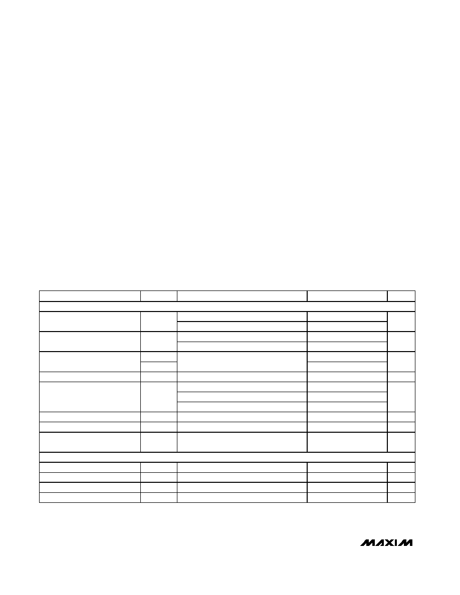
ABSOLUTE MAXIMUM RATINGS
Stresses beyond those listed under "Absolute Maximum Ratings" may cause permanent damage to the device. These are stress ratings only, and functional
operation of the device at these or any other conditions beyond those indicated in the operational sections of the specifications is not implied. Exposure to
absolute maximum rating conditions for extended periods may affect device reliability.
ELECTRICAL CHARACTERISTICS
(V
GATEVSS
= V
AVSS
= -5.5V to -4.75V, V
AVDD
= +4.75V to +5.25V, V
DVDD
= +2.7V to V
AVDD
, external V
REFADC
= +2.5V, external
V
REFDAC
= +2.5V, C
REFADC
= C
REFDAC
= 0.1µF, V
OPSAFE1
= V
OPSAFE2
= 0, V
RCS1+
= V
RCS2+
= +5V, C
FILT1
= C
FILT3
= 1nF, C
FILT2
=
C
FILT4
= 1nF, V
AGND
= V
DGND
= 0, V
ADCIN0
= V
ADCIN1
= 0, V
ACLAMP1
= V
ACLAMP2
= -5V, T
J
= T
MIN
to T
MAX
, unless otherwise noted.
All typical values are at T
J
= +25°C.)
PARAMETER
SYMBOL
CONDITIONS
MIN
TYP
MAX
UNITS
CURRENT-SENSE AMPLIFIER (Note 1)
MAX11014
0.5
11.0
Common-Mode Input Voltage
Range
V
RCS+
MAX11015
5
32
V
0.5V < V
RCS_+
< 11V for the MAX11014
90
Common-Mode Rejection Ratio
CMRR
5V < V
RCS_+
< 32V for the MAX11015
90
dB
I
RCS+
200
Input-Bias Current
I
RCS-
V
SENSE
< 100mV over the common-mode
range
±2
µA
Full-Scale Sense Voltage
V
SENSE
V
SENSE
= V
RCS+
- V
RCS-
625
mV
To within ±0.5% accuracy
75
625
To within ±2% accuracy
20
625
Sense Voltage Range
To within ±20% accuracy
2
625
mV
Total Current Set Error
V
SENSE
= 75mV
±0.1
±0.5
%
Current-Sense Settling Time
t
HSCS
Settles to within ±0.5% of final value
< 25
µs
Saturation Recovery Time
Settles to within ±0.5% accuracy, from
V
SENSE
= 1.875V
< 45
µs
CLASS AB INPUT CHANNEL
Untrimmed Offset
19
Bits
Offset Temperature Coefficient
0
Bits/
o
C
Gain
4
Gain Error
0.1
%
AV
DD
to AGND .........................................................-0.3V to +6V
DV
DD
to DGND.........................................................-0.3V to +6V
AGND to DGND.....................................................-0.3V to +0.3V
AV
SS
to AGND ...........................................................-0.3V to -6V
RCS1+, RCS1-, RCS2+, RCS2- to GATEV
SS
(MAX11014) ........................................................-0.3V to +13V
RCS1+, RCS1-, RCS2+, RCS2- to AGND
(MAX11015) ........................................................-0.3V to +34V
RCS1- to RCS1+.......................................................-6V to +0.3V
RCS2- to RCS2+.......................................................-6V to +0.3V
GATEV
SS
to AGND...................................................+0.3V to -6V
GATE1, GATE2 to AGND .....(GATEV
SS
- 0.3V) to (AV
DD
+ 0.3V)
DV
DD
to AV
DD
..........................................-0.3V to (AV
DD
+ 0.3V)
All Other Analog Inputs to AGND ............-0.3V to (AV
DD
+ 0.3V)
PGAOUT1, PGAOUT2 to AGND ..............-0.3V to (AV
DD
+ 0.3V)
SCLK/SCL, DIN/SDA,
CS/A0, N.C./A2, CNVST, OPSAFE1,
OPSAFE2 to DGND.............................-0.3V to (DV
DD
+ 0.3V)
DOUT/A1, SPI/I2C, ALARM, BUSY
to DGND ..............................................-0.3V to (DV
DD
+ 0.3V)
Maximum Current into Any Pin............................................50mA
Continuous Power Dissipation (T
A
= +70°C)
48-Pin Thin QFN (derate 27.0mW/°C
above +70°C)..........................................................2162.2mW
Operating Temperature Range .........................-40°C to +105°C
Storage Temperature Range ...............................-60°C to 150°C
Junction Temperature ......................................................+150°C
Lead Temperature (soldering, 10s) .................................+300°C
MAX11014/MAX11015
Automatic RF MESFET Amplifier
Drain-Current Controllers
_______________________________________________________________________________________
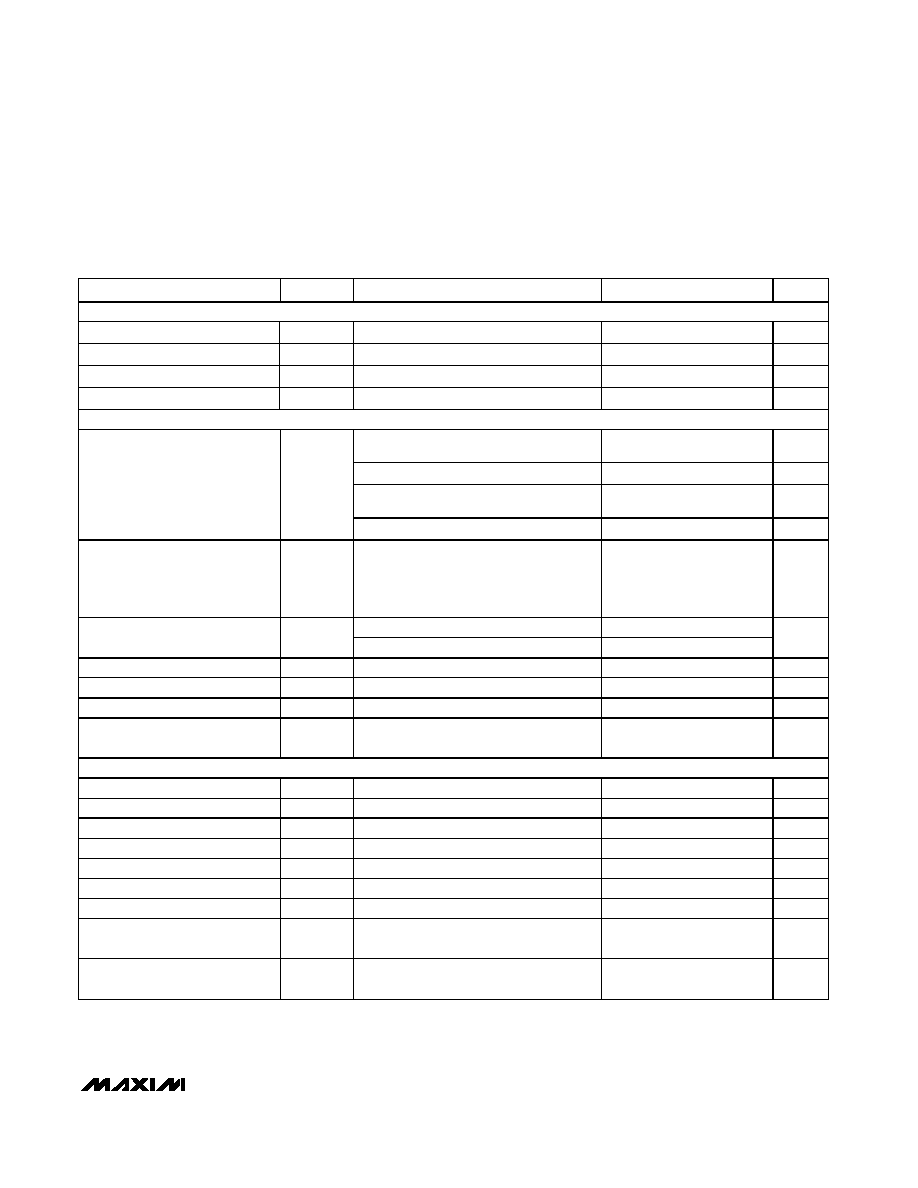
3
PARAMETER
SYMBOL
CONDITIONS
MIN
TYP
MAX
UNITS
CLASS AB OUTPUT CHANNEL
Untrimmed Offset
(Note 1)
50
µV
Offset Temperature Coefficient
0
mV/
o
C
Gain
-2
Gain Error
0.1
%
GATE-DRIVE AMPLIFIER/INTEGRATOR
I
GATE
= -1mA
V
GATEVSS
+
1
V
I
GATE
= +1mA
-0.15
-4
mV
I
GATE
= -10mA
V
GATEVSS
+
1.2
V
Output Gate-Drive Voltage Range
(Note 2)
V
GATE
I
GATE
= +10mA
-1
-20
mV
Gate Voltage Settling Time--
MAX11015
t
GATE
S ettl es to w i thi n ± 0.5% of fi nal val ue, R
S
=
50
, C
GAT E
= 15µF, see GATE O utp ut
Resi stance vs. GATE V ol tag e i n the Typ i cal
O p er ati ng C har acter i sti cs
1.1
ms
No series resistance, R
S
= 0
0
0.5
Output Capacitive Load (Note 3)
C
GATE
R
S
= 500
0
15,000
nF
Gate Voltage Noise
RMS noise, 1kHz to 1MHz
250
nV/
Hz
Maximum Power-On Transient
C
LOAD
= 1nF
±100
mV
Output Short-Circuit Current Limit
I
SC
Sinking or sourcing
±25
mA
Output Safe Switch On-
Resistance
R
OPSW
Clamp GATE1 to ACLAMP1, GATE2 to
ACLAMP2 (Note 4)
3.6
k
ADC DC ACCURACY
Resolution
12
Bits
Differential Nonlinearity
DNL
ADC
No missing codes
±1
LSB
Integral Nonlinearity
INL
ADC
(Note 5)
±1.25
LSB
Offset Error
±2
±4
LSB
Gain Error
(Note 6)
±2
±4
LSB
Gain Temperature Coefficient
±0.4
ppm/
o
C
Offset Temperature Coefficient
±0.4
ppm/
o
C
Channel-to-Channel Offset
Matching
±0.1
LSB
Channel-to-Channel Gain
Matching
±0.1
LSB
ELECTRICAL CHARACTERISTICS (continued)
(V
GATEVSS
= V
AVSS
= -5.5V to -4.75V, V
AVDD
= +4.75V to +5.25V, V
DVDD
= +2.7V to V
AVDD
, external V
REFADC
= +2.5V, external
V
REFDAC
= +2.5V, C
REFADC
= C
REFDAC
= 0.1µF, V
OPSAFE1
= V
OPSAFE2
= 0, V
RCS1+
= V
RCS2+
= +5V, C
FILT1
= C
FILT3
= 1nF, C
FILT2
=
C
FILT4
= 1nF, V
AGND
= V
DGND
= 0, V
ADCIN0
= V
ADCIN1
= 0, V
ACLAMP1
= V
ACLAMP2
= -5V, T
J
= T
MIN
to T
MAX
, unless otherwise noted.
All typical values are at T
J
= +25°C.)
MAX11014/MAX11015
Automatic RF MESFET Amplifier
Drain-Current Controllers
4
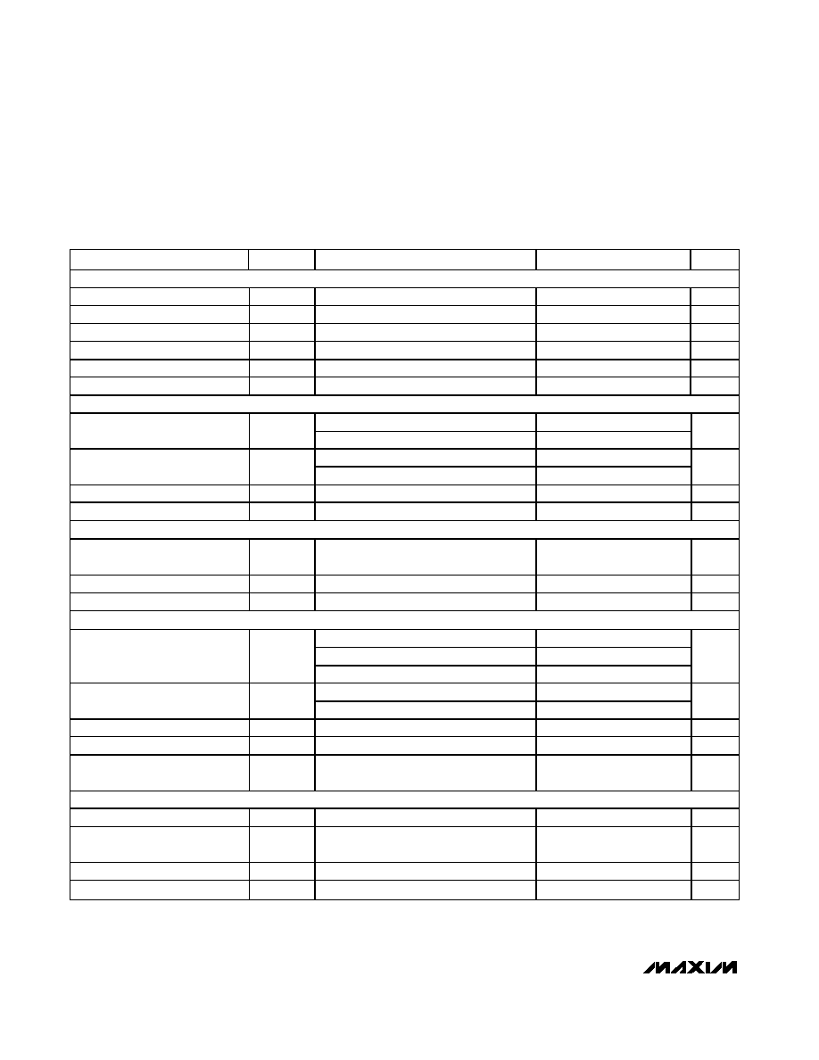
_______________________________________________________________________________________
PARAMETER
SYMBOL
CONDITIONS
MIN
TYP
MAX
UNITS
ADC DYNAMIC ACCURACY (1kHz sine-wave input, -0.5dB from full scale, 94.4ksps)
Signal-to-Noise Plus Distortion
SINAD
70
dB
Total Harmonic Distortion
THD
Up to the 5th harmonic
-84
dB
Spurious-Free Dynamic Range
SFDR
86
dB
Intermodulation Distortion
IMD
f
IN1
= 9.9kHz, f
IN2
= 10.2kHz
76
dB
Full-Power Bandwidth
-3dB point
1
MHz
Full-Linear Bandwidth
S / (N + D) > 68dB
100
kHz
ADC CONVERSION RATE
External reference
0.8
Power-Up Time
t
PU
Internal reference
50
µs
GATE_ and sense voltage measurements
40
Acquisition Time (Note 3)
t
ACQ
All other measurements
1.5
µs
Conversion Time
t
CONV
Internally clocked
6.5
µs
Aperture Delay
30
ns
ADCIN1, ADCIN2 INPUTS
Input Range
V
ADCIN_
Relative to AGND (Note 7)
0
V
REFADC
V
Input Leakage Current
V
ADCIN_
= 0V or V
AVDD
±0.01
±1
µA
Input Capacitance
C
ADCIN_
34
pF
TEMPERATURE MEASUREMENTS
T
J
= +25°C
±0.25
T
J
= -40°C to +85°C (Note 3)
±1.0
±2.5
Internal Sensor Measurement
Error
T
J
= -40°C to +105°C (Note 3)
±1.0
±3.5
°C
T
J
= +25°C
±1.0
External Sensor Measurement
Error (Note 8)
T
J
= -40°C to +105°C
±3
°C
Temperature Resolution
0.125
°C/LSB
External Diode Drive
3.26
75.00
µA
External Temperature Sensor
Drive Current Ratio
16.6
INTERNAL REFERENCE
Reference Output Voltage
V
REFADC
= V
REFDAC
+2.490
+2.500
+2.510
V
Reference Output Temperature
Coefficient
±15
ppm/
o
C
Reference Output Impedance
6.5
k
Power-Supply Rejection Ratio
PSRR
V
AVDD
= +5V ±5%
-83
dB
ELECTRICAL CHARACTERISTICS (continued)
(V
GATEVSS
= V
AVSS
= -5.5V to -4.75V, V
AVDD
= +4.75V to +5.25V, V
DVDD
= +2.7V to V
AVDD
, external V
REFADC
= +2.5V, external
V
REFDAC
= +2.5V, C
REFADC
= C
REFDAC
= 0.1µF, V
OPSAFE1
= V
OPSAFE2
= 0, V
RCS1+
= V
RCS2+
= +5V, C
FILT1
= C
FILT3
= 1nF, C
FILT2
=
C
FILT4
= 1nF, V
AGND
= V
DGND
= 0, V
ADCIN0
= V
ADCIN1
= 0, V
ACLAMP1
= V
ACLAMP2
= -5V, T
J
= T
MIN
to T
MAX
, unless otherwise noted.
All typical values are at T
J
= +25°C.)
MAX11014/MAX11015
Automatic RF MESFET Amplifier
Drain-Current Controllers
_______________________________________________________________________________________
5
PARAMETER
SYMBOL
CONDITIONS
MIN
TYP
MAX
UNITS
EXTERNAL REFERENCES
REFADC Input Voltage Range
V
REFADC
+1.0
V
AVDD
V
V
REFADC
= +2.5V, f
SAMPLE
= 178ksps
60
REFADC Input Current
I
REFADC
Acquisition/between conversions
±0.01
µA
REFDAC Input Voltage Range
V
REFDAC
+0.50
+2.52
V
REFDAC Input Current
26
µA
DAC DC ACCURACY
Resolution
12
Bits
Integral Nonlinearity
INL
DAC
Measured at FILT_
±1
LSB
Differential Nonlinearity
DNL
DAC
Measured at FILT_, guaranteed monotonic
±0.4
±1
LSB
POWER SUPPLIES
Analog Supply Voltage
V
AVDD
+4.75
+5.25
V
Digital Supply Voltage
V
DVDD
+2.7
AV
DD
V
Negative Supply Voltage
V
GATEVSS
,
V
AVSS
V
GATEVSS
= V
AVSS
-5.50
-4.75
V
Analog Supply Current
I
AVDD
V
AVDD
= +5.25V
2.8
5
mA
Digital Supply Current
I
DVDD
V
DVDD
= +5.25V
1.5
5
mA
Negative Supply Current
I
GATEVSS
+ I
AVSS
V
GATEVSS
= V
AVSS
= -5.5V
1.1
1.7
mA
Analog Shutdown Current
V
AVDD
= +5.25V
0.8
µA
Digital Shutdown Current
V
DVDD
= +5.25V
0.2
µA
Negative Shutdown Current
V
GATEVSS
= V
AVSS
= -5.5V
0.6
µA
SERIAL-INTERFACE SUPPLIES
V
IL
0.3 x
DV
DD
Input Voltage
V
IH
0.7 x
DV
DD
V
Input Hysteresis
V
HYS
0.05 x
DV
DD
V
Output Low Voltage
V
OL
BUSY: I
SINK
= 0.5mA;
DOUT, ALARM: I
SINK
= 3mA
0.4
V
Output High Voltage
V
OH
SPI/
I2C = DV
DD
;
BUSY: I
SOURCE
= 0.5mA;
DOUT, ALARM: I
SOURCE
= 2mA
DV
DD
-
0.5V
V
Input Current
I
IN
±0.01
±10
µA
Input Capacitance
C
IN
5
pF
ELECTRICAL CHARACTERISTICS (continued)
(V
GATEVSS
= V
AVSS
= -5.5V to -4.75V, V
AVDD
= +4.75V to +5.25V, V
DVDD
= +2.7V to V
AVDD
, external V
REFADC
= +2.5V, external
V
REFDAC
= +2.5V, C
REFADC
= C
REFDAC
= 0.1µF, V
OPSAFE1
= V
OPSAFE2
= 0, V
RCS1+
= V
RCS2+
= +5V, C
FILT1
= C
FILT3
= 1nF, C
FILT2
=
C
FILT4
= 1nF, V
AGND
= V
DGND
= 0, V
ADCIN0
= V
ADCIN1
= 0, V
ACLAMP1
= V
ACLAMP2
= -5V, T
J
= T
MIN
to T
MAX
, unless otherwise noted.
All typical values are at T
J
= +25°C.)