General Description
The MAX11041/MAX11042 wired remote controllers
convert up to six or 30 different pushbuttons into an
I
2
C* register. Together with low-cost pushbutton switch-
es and 1% resistors, the MAX11041/MAX11042 are
total solutions over a single-wire interface. A wired
remote controller easily piggybacks to a standard
3.5mm headphone jack using a fourth contact or one of
the audio signals.
To conserve battery life, the MAX11041/MAX11042
consume only 5µA (typ) while reading keypresses in
real time without microprocessor (µP) polling. The
devices send the debounced keypress along with key
duration to the application processor over the I
2
C inter-
face. An 8-word FIFO buffer records up to four key-
press events to allow plenty of time for the application
processor to respond to the MAX11041/MAX11042.
The MAX11041/MAX11042 include ±15kV ESD protec-
tion devices on the FORCE and SENSE inputs to ensure
IEC 61000-4-2 compliance without any external
ESD devices.
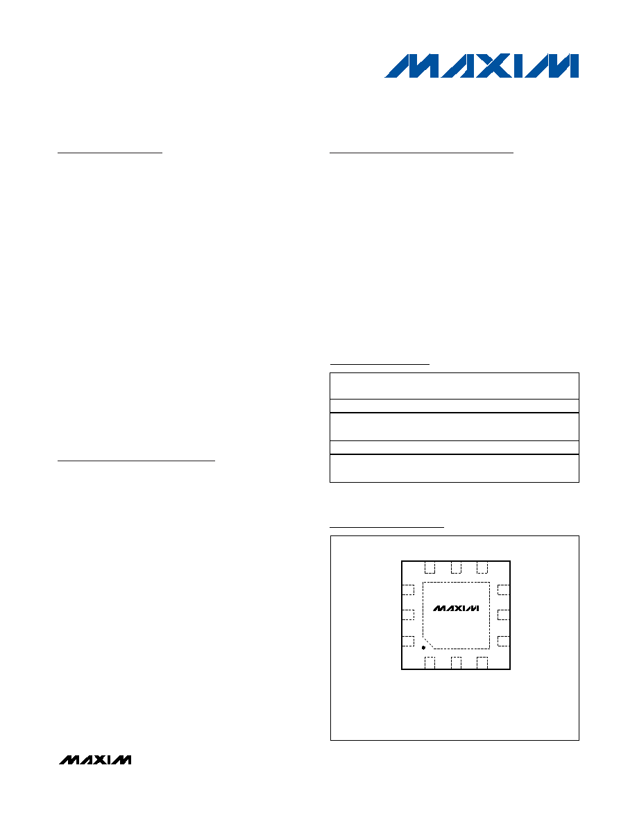
The MAX11041/MAX11042 are available in 12-bump
UCSPTM and 12-pin TQFN packages. The devices are
specified over the extended temperature range
(-40∞C to +85∞C).
Applications
Features
Detect Up to Six (MAX11042) or 30 (MAX11041)
Different Keys and Jack Insertion/Removal
Work with Either 32 or 16 Headphones
Add Remote-Control Functionality to Devices
Using a Simple Resistor and Switch Array
Low-Power Operation Consuming a Supply
Current of Only 5µA (typ)
Work with Standard 2.5mm or 3.5mm 4-Pin
Headphone Jacks
Support Hold Function to Lockout Keys
100kHz/400kHz I
2
C Interface
Single 1.6V to 3.6V Supply Voltage Range
±15kV ESD Protection (IEC 61000-4-2)
MAX11041/MAX11042
Wired Remote Controllers
________________________________________________________________ Maxim Integrated Products
1
19-3984; Rev 0; 1/06
For pricing, delivery, and ordering information, please contact Maxim/Dallas Direct! at
1-888-629-4642, or visit Maxim's website at www.maxim-ic.com.
12
11
10
4
5
SENSE
V
DD
6
GND
SCL
SHDN
SDA
1
2
V
DD
3
9
8
7
FORCE
A0
A1
N.C.
MAX11041
MAX11042
INT
THIN QFN
(4mm x 4mm x 0.6mm)
TOP VIEW
EXPOSED PAD CONNECTED TO GND.
Pin Configurations
Ordering Information
UCSP is a trademark of Maxim Integrated Products, Inc.
*Purchase of I
2
C components from Maxim Integrated Products,
Inc., or one of its sublicensed Associated Companies, conveys
a license under the Philips I
2
C Patent Rights to use these com-
ponents in an I
2
C system, provided that the system conforms
to the I
2
C Standard Specification as defined by Philips.
*EP = Exposed pad.
**Future product--contact factory for availability.
Pin Configurations continued at end of data sheet.
Multimedia Controls for
Multimedia-Enabled
Cell Phones
Keyboard Encoder for
Slider, Flip, and other
Cell Phones
Portable Media Players
MP3, CD, DVD Players
PDAs
Digital Still Cameras
PDA Accessory
Keyboards
Multimedia Desktop
Speakers
Portable Game
Consoles
PART
TEMP
RANGE
PIN-
PACKAGE
PKG
CODE
MAX11041ETC
-40∞C to +85∞C 12 TQFN-EP*
T1244-4
M AX 11041E BC - T**
-40∞C to +85∞C
12 UCSP
(4 x 4 Array)
B16-5
MAX11042ETC**
-40∞C to +85∞C 12 TQFN-EP*
T1244-4
M AX 11042E BC - T**
-40∞C to +85∞C
12 UCSP
(4 x 4 Array)
B16-5

MAX11041/MAX11042
Wired Remote Controllers
2
_______________________________________________________________________________________
ABSOLUTE MAXIMUM RATINGS
Stresses beyond those listed under "Absolute Maximum Ratings" may cause permanent damage to the device. These are stress ratings only, and functional
operation of the device at these or any other conditions beyond those indicated in the operational sections of the specifications is not implied. Exposure to
absolute maximum rating conditions for extended periods may affect device reliability.
V
DD
to GND ...........................................................-0.3V to +4.0V
INT to GND .................................................-0.3V to (V
DD
+ 0.3V)
SCL, SDA, A1, A0, SHDN to GND.........................-0.3V to +4.0V
FORCE, SENSE to GND.........................................................±6V
Current into Any Pin..........................................................±50mA
Maximum ESD per IEC 61000-4-2
Human Body Model, FORCE, SENSE............................±15kV
FORCE, SENSE Short to GND....................................Continuous
Junction Temperature ......................................................+150∞C
Operating Temperature Range ...........................-40∞C to +85∞C
Storage Temperature Range .............................-65∞C to +150∞C
Lead Temperature (soldering, 10s) .................................+300∞C
ELECTRICAL CHARACTERISTICS
(V
DD
= +1.6V to 3.6V, C
SENSE
= 10nF, R
SENSE
= 10k
, T
A
= T
MIN
to T
MAX
, unless otherwise noted. Typical values are at T
A
= +25∞C.)
PARAMETER
SYMBOL
CONDITIONS
MIN
TYP
MAX
UNITS
KEY DETECTION CHARACTERISTICS
MAX11041
30
Detectable Keys
Provided the keys meet
the next three
specifications; R
JACK
connected; use
recommended circuit
MAX11042
6
Keys
Maximum Switch Resistance
(Note 1)
100
Maximum Switch Bounce Time
(Note 1)
13
ms
External Resistor Tolerance
(Note 1)
±1
%
SWITCH DEBOUNCE
Debounce Analog Time Constant
C
SENSE
= 10nF, external resistor from
FORCE to SENSE is 10k
(R
SENSE
)
0.4
ms
Chatter Rejection
Pulses shorter than this are ignored
18
ms
Rising Voltage Debounce Time
t
CPW
Time required for a new voltage (due to
keypress) to be detected and stored in
FIFO
18
ms
Falling Voltage Debounce Time
t
LPWS
Time required for detection of key release
and final time duration to be stored in FIFO
18
ms
Jack Insertion Debounce Time
(Note 2)
18
ms
Jack Removal Debounce Time
(Note 2)
18
ms
DURATION COUNTER
Duration-Counter Resolution
One tick
32
ms
Duration-Counter Range
MSB is overflow bit
0
127
Counts
Duration-Counter Accuracy
±20
%
DIGITAL INPUTS (SDA, SCL,
SHDN, A0, A1)
Input High Voltage
V
IH
0.7 x
V
DD
V
Input Low Voltage
V
IL
0.3 x
V
DD
V
Input Leakage Current
I
IH
, I
IL
-10
+10
µA
Input Hysteresis
9
%V
DD
Input Capacitance
10
pF
MAX11041/MAX11042
Wired Remote Controllers
ELECTRICAL CHARACTERISTICS (continued)
(V
DD
= +1.6V to 3.6V, C
SENSE
= 10nF, R
SENSE
= 10k
, T
A
= T
MIN
to T
MAX
, unless otherwise noted. Typical values are at T
A
= +25∞C.)
PARAMETER
SYMBOL
CONDITIONS
MIN
TYP
MAX
UNITS
DIGITAL OUTPUTS (SDA,
INT)
Output High Voltage (INT)
V
OH
I
SOURCE
2mA
0.9 x
V
DD
V
Output Low Voltage (INT)
V
OLINT
I
SINK
2mA
0.1 x
V
DD
V
Output High Leakage Current
I
OHL
V
OUT
= V
DD
1
µA
I
OL
= 3mA for V
DD
> 2V
0.4
V
Output Low Voltage (SDA)
V
OLSDA
I
OL
= 3mA for V
DD
< 2V
0.2 x
V
DD
V
I2C TIMING CHARACTERISTICS (see Figure 1)
Serial Clock Frequency
f
SCL
0
400
kHz
Bus Free Time Between STOP
and START Conditions
t
BUF
1.3
µs
Hold Time (Repeated) START
Condition
t
HD,STA
0.6
µs
SCL Pulse-Width Low
t
LOW
1.3
µs
SCL Pulse-Width High
t
HIGH
0.6
µs
Setup Time for a Repeated
START Condition
t
SU,STA
0.6
µs
Data Hold Time
t
HD,DAT
0
900
ns
Data Setup Time
t
SU,DAT
100
ns
SDA and SCL Receiving Rise
Time
t
RR
(Note 3)
20 +
C
b
/ 10
300
ns
SDA and SCL Receiving Fall
Time
t
FR
(Note 3)
20 +
C
b
/ 10
300
ns
SDA Transmitting Rise Time
t
RT
V
DD
= 3.6V (Note 3)
20 +
C
b
/ 10
250
ns
V
DD
= 2.4V to 3.6V
20 +
C
b
/ 20
250
SDA Transmitting Fall Time
t
FT
V
DD
= 1.6V to 2.4V
20 +
C
b
/ 20
375
ns
Setup Time for STOP Condition
t
SU,STO
0.6
µs
Bus Capacitance
C
b
400
pF
Pulse Width of Suppressed Spike
t
SP
0
50
ns
____________________________________________________________________________________
3
MAX11041/MAX11042
Wired Remote Controllers
4
_______________________________________________________________________________________
Note 1: Recommended properties of external switch for proper detection of 30 keys or key combinations.
Note 2: See the Jack Insertion/Removal Detection section.
Note 3: C
b
is the bus capacitance in pF.
Note 4: Key current depends on external key resistors and is calculated by V
DD
/ (30.1k
+ R
SW
).
Figure 1. I
2
C Serial-Interface Timing
ELECTRICAL CHARACTERISTICS (continued)
(V
DD
= +1.6V to 3.6V, C
SENSE
= 10nF, R
SENSE
= 10k
, T
A
= T
MIN
to T
MAX
, unless otherwise noted. Typical values are at T
A
= +25∞C.)
PARAMETER
SYMBOL
CONDITIONS
MIN
TYP
MAX
UNITS
POWER SUPPLIES
Power-Supply Voltage
V
DD
1.6
3.6
V
Excluding jack/key current
5
20
Average Operational Supply
Current
I
DDOP
Jack inserted, R
JACK
= 619k
8
µA
Shutdown Power-Supply Current
I
DDSHDN
Excluding jack/key current
1
µA
Jack Current
I
DDJACK
Flowing when jack is inserted
4
µA
Key Current
I
DDBUTTON
Flowing when keys pressed (Note 4)
90
µA
SHDN High to Part Active
Wake-up time
5
ms
t
HD,STA
t
SU,DAT
SDA
t
HD,DAT
SCL
STOP CONDITION
(P)
t
SU,STA
t
SU,STO
t
LOW
t
BUF
START CONDITION
(S)
t
HD,STA
t
HIGH
t
RR,
t
RT
t
FR,tFT
t
RR
t
FR
START CONDITION
(S)
REPEAT START CONDITION
(Sr)

MAX11041/MAX11042
Wired Remote Controllers
10ms/div
V
SENSE
INT
MAX11041/42 TOC01
µP READS FIFO
DEBOUNCED KEY
ADDED TO FIFO
DEBOUNCE SCOPE SHOT (FALLING)
10ms/div
V
SENSE
INT
MAX11041/42 TOC02
µP READS
FIFO
DEBOUNCE KEY ADDED
TO FIFO
DEBOUNCE SCOPE SHOT (RISING)
10ms/div
V
SENSE
INT
MAX11041/42 TOC03
µP READS
FIFO
DEBOUNCE KEY ADDED
TO FIFO
KEYPRESS RELEASE SCOPE SHOT*
4.0
5.0
4.5
6.0
5.5
6.5
7.0
1.6
2.6
2.1
3.1
3.6
V
DD
SUPPLY CURRENT vs. VOLTAGE
MAX11041/42 TOC04
V
DD
(V)
I
DD
(
µ
A)
NO JACK INSERTED
T
A
= +85
∞C
T
A
= +25
∞C
T
A
= -40
∞C
1.00
0.75
0.50
0.25
0
1.6
2.6
2.1
3.1
3.6
V
DD
SHUTDOWN SUPPLY CURRENT
vs. VOLTAGE
MAX11041/42 TOC05
V
DD
(V)
I
DD
(
µ
A)
NO JACK INSERTED
T
A
= +85
∞C
T
A
= -40
∞C
T
A
= +25
∞C
Typical Operating Characteristics
(T
A
= +25∞C, unless otherwise noted.)
____________________________________________________________________________________
5
*Oscilloscope shots are taken with simulated bounce and chatter. Real switches will exhibit different bounce and chatter characteristics.