Äîêóìåíòàöèÿ è îïèñàíèÿ www.docs.chipfind.ru
General Description
The MAX1115/MAX1116 low-power, 8-bit, analog-to-
digital converters (ADCs) feature an internal track/hold
(T/H), voltage reference, V
DD
monitor, clock, and serial
interface. The MAX1115 is specified from +2.7V to
+5.5V, and the MAX1116 is specified from +4.5V to
+5.5V. Both parts consume only 175µA at 100ksps.
The full-scale analog input range is determined by the
internal reference of +2.048V (MAX1115) or +4.096V
(MAX1116). The MAX1115/MAX1116 also feature
AutoShutdownTM power-down mode which reduces
power consumption to <1µA when the device is not in
use. The 3-wire serial interface directly connects to
SPITM, QSPITM, and MICROWIRETM devices without
external logic. Conversions up to 100ksps are per-
formed using an internal clock.
The MAX1115/MAX1116 are available in an 8-pin
SOT23 package with a footprint that is just 30% of an
8-pin SO.
________________________Applications
Low-Power, Hand-Held Portable Devices
System Diagnostics
Battery-Powered Test Equipment
Receive-Signal-Strength Indicators
4mA to 20mA Powered Remote Data-Acquisition
Systems
Features
o Single Supply
+2.7V to +3.6V (MAX1115)
+4.5V to +5.5V (MAX1116)
o Input Voltage Range: 0 to V
REF
o Internal Track/Hold; 100kHz Sampling Rate
o Internal Reference
+2.048V (MAX1115)
+4.096V (MAX1116)
o SPI/QSPI/MICROWIRE-Compatible Serial Interface
o Small 8-Pin SOT23 Package
o Automatic Power-Down
o Low Power
175µA at 100ksps
18µA at +3V and 10ksps
1µA in Power-Down Mode
MAX1115/MAX1116
Single-Supply, Low-Power, Serial 8-Bit ADCs
________________________________________________________________ Maxim Integrated Products
1
1
2
3
4
8
7
6
5
SCLK
DOUT
CONVST
GND
I.C.
CH0
V
DD
MAX1115
MAX1116
SOT23
TOP VIEW
I.C.
Pin Configuration
19-1822; Rev 1; 2/02
Ordering Information
PART
TEMP RANGE
PIN-
PA CK A G E
TO P
M A RK
MAX1115EKA
-40°C to +85°C
8 SOT23
AADU
MAX1116EKA
-40°C to +85°C
8 SOT23
AADV
AutoShutdown is a trademark of Maxim Integrated Products.
SPI/QSPI are trademarks of Motorola, Inc.
MICROWIRE is a trademark of National Semiconductor, Corp.
For pricing, delivery, and ordering information, please contact Maxim/Dallas Direct! at
1-888-629-4642, or visit Maxim's website at www.maxim-ic.com.
MAX1115/MAX1116
Single-Supply, Low-Power, Serial 8-Bit ADCs
2
_______________________________________________________________________________________
ABSOLUTE MAXIMUM RATINGS
ELECTRICAL CHARACTERISTICS
(V
DD
= +2.7V to +3.6V (MAX1115), V
DD
= +4.5V to +5.5V (MAX1116), T
A
= T
MIN
to T
MAX
, unless otherwise noted.)
Stresses beyond those listed under "Absolute Maximum Ratings" may cause permanent damage to the device. These are stress ratings only, and functional
operation of the device at these or any other conditions beyond those indicated in the operational sections of the specifications is not implied. Exposure to
absolute maximum rating conditions for extended periods may affect device reliability.
V
DD
to GND ...........................................................-0.3V to +6.0V
CH0 to GND ...............................................-0.3V to (V
DD
+ 0.3V)
Digital Output to GND ................................-0.3V to (V
DD
+ 0.3V)
Digital Input to GND ..............................................-0.3V to +6.0V
Maximum Current into Any Pin .........................................±50mA
Continuous Power Dissipation (T
A
= +70°C)
8-Pin SOT23 (derate 8.9mW/°C above +70°C)............714mW
Operating Temperature Range
MAX111_EKA ..................................................-40°C to + 85°C
Junction Temperature ......................................................+150°C
Storage Temperature Range .............................-60°C to +150°C
Lead Temperature (soldering, 10s) .................................+300°C
PARAMETER
SYMBOL
CONDITIONS
MIN
TYP
MAX
UNITS
DC ACCURACY
Resolution
8
Bits
Relative Accuracy
INL
(Note 1)
±1
LSB
Differential Nonlinearity
DNL
±1
LSB
Offset Error
0.5
LSB
Gain Error
±5
%FSR
Gain Temperature Coefficient
90
ppm/
°C
V
DD
/2 Sampling Error
±2
±7
%
DYNAMIC PERFORMANCE (25kHz sine-wave input, V
IN
= V
REF
(
P-P
), f
SCLK
= 5MHz, f
SAMPLE
= 100ksps, R
IN
= 100
)
Signal-to-Noise Plus Distortion
SINAD
48
dB
Total Harmonic Distortion
(up to the 5th Harmonic)
THD
-69
dB
Spurious-Free Dynamic Range
SFDR
66
dB
Small-Signal Bandwidth
f
-3dB
4
MHz
ANALOG INPUT
Input Voltage Range
0
V
REF
V
Input Leakage Current
V
CH
= 0 or V
DD
±0.7
±10
µA
Input Capacitance
C
IN
18
pF
INTERNAL REFERENCE
MAX1115
2.048
Voltage
V
REF
MAX1116
4.096
V
POWER REQUIREMENTS
MAX1115
2.7
5.5
Supply Voltage
V
DD
MAX1116
4.5
5.5
V
f
SAMPLE
= 10ksps
14
21
MAX1115
f
SAMPLE
= 100ksps
135
190
f
SAMPLE
= 10ksps
19
25
MAX1116
f
SAMPLE
= 100ksps
182
230
Supply Current (Note 2)
I
DD
Shutdown
0.8
10
µA
MAX1115/MAX1116
Single-Supply, Low-Power, Serial 8-Bit ADCs
_______________________________________________________________________________________
3
Note 1: Relative accuracy is the deviation of the analog value at any code from its theoretical value after the full-scale range and off-
set have been calibrated.
Note 2: Input = 0, with logic input levels of 0 and V
DD
.
PARAMETER
SYMBOL
CONDITIONS
MIN
TYP
MAX
UNITS
Supply Rejection Ratio
PSRR
Full-scale or zero input
±0.5
±1
LSB/V
DIGITAL INPUTS (CNVST AND SCLK)
Input High Voltage
V
IH
2
V
Input Low Voltage
V
IL
0.8
V
Input Hystersis
V
HYST
0.2
V
Input Current High
I
IH
±10
µA
Input Current Low
I
IL
±10
µA
Input Capacitance
C
IN
2
pF
DIGITAL OUTPUT (DOUT)
Output High Voltage
V
OH
I
SOURCE
= 2mA
V
DD
- 0.5
V
I
SINK
= 2mA
0.4
Output Low Voltage
V
OL
I
SINK
= 4mA
0.8
V
Three-State Leakage Current
I
L
±0.01
±10
µA
Three-State Output Capacitance
C
OUT
4
pF
TIMING CHARACTERISTICS (Figures 6a6d)
CNVST High Time
t
csh
100
ns
CNVST Low Time
t
csl
100
ns
Conversion Time
t
conv
7.5
µs
Serial Clock High Time
t
ch
75
ns
Serial Clock Low Time
t
cl
75
ns
Serial Clock Period
t
cp
200
ns
Falling of CNVST to DOUT
Active
t
csd
C
LOAD
= 100pF, Figure 1
100
ns
Serial Clock Falling Edge to
DOUT
t
cd
C
LOAD
= 100pF
10
100
ns
Serial Clock Rising Edge
To DOUT High-Z
t
chz
C
LOAD
= 100pF, Figure 2
100
500
ns
Last S er i al C l ock to N ext C N V S T
( successi ve conver si ons on C H 0)
t
ccs
50
ns
ELECTRICAL CHARACTERISTICS (continued)
(V
DD
= +2.7V to +3.6V (MAX1115), V
DD
= +4.5V to +5.5V (MAX1116), T
A
= T
MIN
to T
MAX
, unless otherwise noted.)
MAX1115/MAX1116
Single-Supply, Low-Power, Serial 8-Bit ADCs
4
_______________________________________________________________________________________
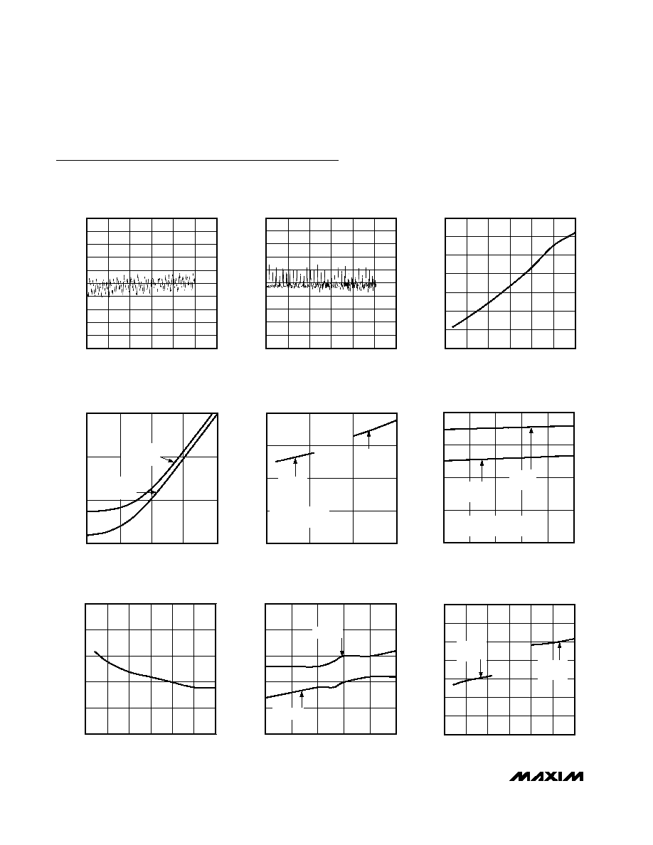
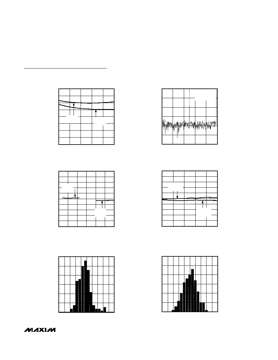
Typical Operating Characteristics
(V
DD
= +3V (MAX1115), V
DD
= +5V (MAX1116), fscu = 5MHz, fsample = 100ksps, C
LOAD
= 100pF, T
A
= +25°C, unless otherwise
noted.)
-1.0
-0.4
-0.6
-0.8
-0.2
0
0.2
0.4
0.6
0.8
1.0
0
100
50
150
200
250
300
INTEGRAL NONLINEARITY
vs. OUTPUT CODE
MAX1115 toc01
OUTPUT CODE
INL (LSB)
-0.2
-0.4
-0.6
0
0.2
0.4
0.6
0.8
1.0
0
100
50
150
200
250
300
DIFFERENTIAL NONLINEARITY
vs. OUTPUT CODE
MAX1115 toc02
OUTPUT CODE
DNL (LSB)
-0.8
-1.0
0
0.2
0.1
0.4
0.3
0.6
0.5
0.7
SHUTDOWN SUPPLY CURRENT
vs. SUPPLY VOLTAGE
MAX1115 toc03
SUPPLY VOLTAGE (V)
SHUTDOWN CURRENT (
µ
A)
2.5
3.5
4.5
5.5
100.0
0
0.01
0.1
1
10
100
SUPPLY CURRENT vs.
CONVERSION RATE
1.0
MAX1115 toc04
CONVERSION (ksps)
SUPPLY CURRENT (
µ
A)
10.0
MAX1116
V
DD
= +5V
MAX1115
V
DD
= +3V
0
50
100
150
200
2.5
3.5
4.5
5.5
SUPPLY CURRENT
vs. SUPPLY VOLTAGE
MAX1115 toc05
SUPPLY VOLTAGE (V)
SUPPLY CURRENT (
µ
A)
MAX1115
MAX1116
D
OUT
= 00000000
V
DD
= V
DIGITAL INPUTS
0
50
100
150
200
-40
-15
10
35
60
85
SUPPLY CURRENT
vs. TEMPERATURE
MAX1115 toc06
TEMPERATURE (
°C)
SUPPLY CURRENT (
µ
A)
D
OUT
= 00000000
V
DD
= V
REF
= V
DIGITAL INPUTS
MAX1115
V
DD
= +3V
MAX1116
V
DD
= +5V
5.0
5.2
5.3
5.1
5.4
5.5
2.5
3.5
4.5
5.5
CONVERSION TIME
vs. SUPPLY VOLTAGE
MAX1115 toc07
SUPPLY VOLTAGE (V)
CONVERSION TIME (
µ
s)
MAX1115 toc08
5.0
5.2
5.3
5.1
5.4
5.5
-40
-15
10
35
60
85
CONVERSION TIME
vs. TEMPERATURE
TEMPERATURE (
°C)
CONVERSION TIME (
µ
s)
V
DD
= +3V
V
DD
= +5V
0
0.6
0.8
0.4
0.2
1.2
1.0
1.4
2.5
4.5
3.5
5.5
GAIN ERROR vs.
SUPPLY VOLTAGE
MAX1115 toc09
SUPPLY VOLTAGE (V)
GAIN ERROR (%FSR)
MAX1116
V
DD
= +5V
MAX1115
V
DD
= +3V
MAX1115/MAX1116
Single-Supply, Low-Power, Serial 8-Bit ADCs
_______________________________________________________________________________________
5
MAX1115 toc10
-2.0
0
0.5
-1.0
-0.5
-1.5
1.5
1.0
2.0
-40
60
35
10
-15
85
GAIN ERROR
vs. TEMPERATURE
TEMPERATURE (
°C)
GAIN ERROR (%FSR)
MAX1116
V
DD
= +5V
MAX1115
V
DD
= +3V
-120
-80
-100
-60
-40
-20
0
0
20k
10k
30k
40k
50k
FFT PLOT
MAX1115 toc11
ANALOG INPUT FREQUENCY (Hz)
AMPLITUDE (dB)
f
SAMPLE
= 100kHz
f
IN
= 25.1kHz
A
IN
= 0.9xV
REF
p-p
-0.5
0
-0.1
0.1
-0.2
-0.3
-0.4
0.3
0.2
0.4
0.5
2.5
3.0
4.0
5.0
4.5
3.5
5.5
OFFSET ERROR vs.
SUPPLY VOLTAGE
MAX1115 toc12
SUPPLY VOLTAGE (V)
OFFSET ERROR (LSB)
MAX1116
VDD = +3V
MAX1115
VDD = +3V
-0.5
0
-0.1
0.1
-0.2
-0.3
-0.4
0.3
0.2
0.4
0.5
-40
-15
60
35
10
85
OFFSET ERROR vs.
TEMPERATURE
MAX1115 toc13
TEMPERATURE (
°C)
OFFSET ERROR (LSB)
MAX1116
VDD = +3V
MAX1115
VDD = +5V
0
10.5%
7.0%
3.5%
17.5%
21.0%
14.0%
1.982
2.008
2.086
2.060
2.034
2.112
MAX1115
REFERENCE VOLTAGE
vs. NUMBER OF PIECES
MAX1115 toc14
REFERENCE VOLTAGE (V)
0
7.0%
3.5%
14.0%
10.5%
17.5%
3.980
4.020
4.140
4.100
4.060
4.180
MAX1116
REFERENCE VOLTAGE
vs. NUMBER OF PIECES
MAX1115 toc15
REFERENCE VOLTAGE (V)
21.0%
Typical Operating Characteristics (continued)
(V
DD
= +3V (MAX1115), V
DD
= +5V (MAX1116), fscu = 5MHz, fsample = 100ksps, C
LOAD
= 100pF, T
A
= +25°C, unless otherwise
noted.)