
_______________General Description
The MAX1125 is a monolithic, flash analog-to-digital con-
verter (ADC) capable of digitizing a 2V analog input signal
into 8-bit digital words at a typical 300Msps update rate.
For most applications, no external sample-and-hold is
required for accurate conversion due to the device's
narrow aperture time, wide bandwidth, and low input
capacitance. A single standard -5.2V power supply is
required to operate the MAX1125, with nominal 2.2W
power dissipation. A special decoding scheme reduces
metastable errors to 1LSB.
The part is packaged in a 42-pin ceramic sidebraze
that is pin compatible with the CX20116 and
CX41396D. The surface-mount 44-pin CERQUAD pack-
age allows access to additional reference ladder taps,
an overrange bit, and a data-ready output. The pin-
compatible 150Msps MAX1114 is also available.
________________________Applications
Digital Oscilloscopes
Transient Capture
Radar, EW, ECM
Direct RF Down-Conversion
Medical Electronics
Ultrasound, CAT Instrumentation
____________________________Features
o
Metastable Errors Reduced to 1LSB
o
10pF Input Capacitance
o
210MHz Input Bandwidth
o
300Msps Conversion Rate
o
2.2W Typical Power Dissipation
o
Single -5.2V Supply
MAX1125
8-Bit, 300Msps Flash ADC
________________________________________________________________
Maxim Integrated Products
1
19-1100; Rev 0; 6/96
For free samples & the latest literature: http://www.maxim-ic.com, or phone 1-800-998-8800
Functional Diagram appears at end of data sheet.
______________Ordering Information
____Pin Configurations (continued)
_________________Pin Configurations
42
41
40
39
38
37
36
35
34
33
32
31
30
29
28
27
26
25
24
23
22
1
2
3
4
5
6
7
8
9
10
11
12
13
14
15
16
17
18
19
20
21
V
EE
N.C.
LINV
V
EE
AGND
DGND
DO (LSB)
D1
D2
D3
D4
D5
D6
D7 (MSB)
DGND
AGND
V
EE
MINV
N.C.
CLK
CLK
N.C.
VRTF
N.C.
V
EE
V
EE
N.C.
N.C.
AGND
VIN
AGND
VR2
AGND
VIN
AGND
N.C.
N.C.
V
EE
V
EE
N.C.
VRBF
N.C.
TOP VIEW
Ceramic SB
MAX1125
MAX1125
CERQUAD
23
24
25
26
27
28
29
30
31
32
V
EE
LINV
N.C.
DRINV
N.C.
V
EE
AGND
AGND
VRTS
VRTF
33
AGND
2
3
4
5
6
7
8
9
10
11
VRBF
VRBS
AGND
AGND
V
EE
CLK
CLK
MINV
V
EE
AGND
1
DGND
38
39
40
41
42
34
35
36
37
43
44
D7
D6
D5
D4
D3
D2
D1
D0 (LSB)
DREADY
DGND
D8 (MSB)
15
18
20
19
21
22
16
17
13
14
AGND
VR1
AGND
VIN
AGND
VR2
AGND
VIN
V
EE
VR3
12
V
EE
TOP VIEW
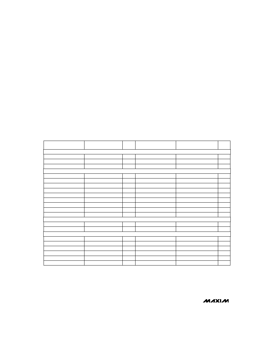
PART
MAX1125AIDO
MAX1125BIDO
MAX1125AIBH
-20∞C to +85∞C
-20∞C to +85∞C
-20∞C to +85∞C
TEMP. RANGE PIN-PACKAGE
42 Ceramic SB
42 Ceramic SB
44 CERQUAD
MAX1125BIBH
-20∞C to +85∞C 44 CERQUAD
±1
±0.75
±1
±0.75
INL (LSBs)
EVALUATION KIT
AVAILABLE
MAX1125
8-Bit, 300Msps Flash ADC
2
_______________________________________________________________________________________
ABSOLUTE MAXIMUM RATINGS
ELECTRICAL CHARACTERISTICS
(V
EE
= -5.2V, R
SOURCE
= 50
, VRBF = -2.00V, VR2 = -1.00V, VRTF = 0.00V, f
CLK
= 150MHz, 50% Duty Cycle, T
A
= T
MIN
to T
MAX
,
unless otherwise noted.)
Stresses beyond those listed under "Absolute Maximum Ratings" may cause permanent damage to the device. These are stress ratings only, and functional
operation of the device at these or any other conditions beyond those indicated in the operational sections of the specifications is not implied. Exposure to
absolute maximum rating conditions for extended periods may affect device reliability.
Negative Supply Voltage (V
EE
TO GND) ..............-7.0V to +0.5V
Ground Voltage Differential ...................................-0.5V to +0.5V
Analog Input Voltage ...............................................V
EE
to +0.5V
Reference Input Voltage ..........................................V
EE
to +0.5V
Digital Input Voltage ................................................V
EE
to +0.5V
Reference Current V
RTF
to V
RBF
........................................25mA
Digital Output Current ...........................................0mA to -30mA
Operating Temperature Range ...........................-25∞C to +85∞C
Junction Temperature ......................................................+150∞C
Storage Temperature Range .............................-65∞C to +150∞C
Lead Temperature (soldering, 10sec). ............................+300∞C
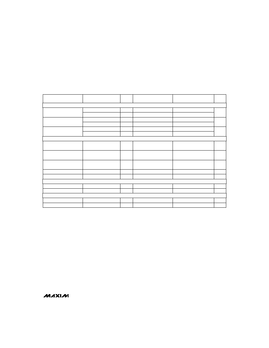
V
V
V
VI
V
V
VI
VI
V
VI
VI
V
V
V
VI
IV
V
IV
V
TEST
LEVEL
ns
1.5
Acquisition Time
ps
5
Aperture Jitter
ns
2.0
CLK-to-Data Ready Delay (t
D
)
ps/∞C
2
Output Delay TEMPCO
ns
2.4
Clock to Data Delay
Msps
250
300
Maximum Sample Rate
MHz
10
Reference Bandwidth
100
200
300
Ladder Resistance
MHz
335
IN = 500mVp-p
Small Signal Bandwidth
MHz
210
VIN = full scale
Large Signal Bandwidth
V/µs
1,000
Input Slew Rate
LSB
-0.75
+0.75
Differential Linearity
LSB
-0.75
±0.60
+0.75
Integral Linearity
µA
250
500
Input Current
k
15
Input Resistance
pF
10
Over full input range
Input Capacitance
V
-2.0
0.0
Input Voltage Range
Guaranteed
No Missing Codes
mV
-30
+30
Offset Error V
RT
mV
-30
+30
Offset Error V
RB
UNITS
MAX1125A
MIN
TYP
MAX
CONDITIONS
PARAMETER
1.5
5
2.0
2
2.4
250
300
10
100
200
300
335
210
1,000
-0.95
+0.95
-0.95
±0.80
+0.95
250
500
15
10
-2.0
0.0
Guaranteed
-30
+30
-30
+30
MAX1125B
MIN
TYP
MAX
DC ACCURACY
ANALOG INPUT
REFERENCE INPUT
TIMING CHARACTERISTICS
MAX1125
8-Bit, 300Msps Flash ADC
_______________________________________________________________________________________
3
ELECTRICAL CHARACTERISTICS (continued)
(V
EE
= -5.2V, R
SOURCE
= 50
, VRBF = -2.00V, VR2 = -1.00V, VRTF = 0.00V, f
CLK
= 150MHz, 50% Duty Cycle, T
A
= T
MIN
to T
MAX
,
unless otherwise noted.)
I
VI
I
V
VI
VI
VI
VI
VI
VI
VI
VI
VI
VI
V
VI
TEST
LEVEL
W
2.2
2.9
T
A
= +25 ∞C
Power Dissipation
mA
425
550
T
A
= +25 ∞C
Supply Current
ns
2.4
V
-1.5
50
to -2V
Digital Output Low Voltage
V
-1.1
50
to -2V
Digital Output High Voltage
ns
2
1.8
Clock High Width, T
PWH
ns
2
1.8
Clock Low Width, T
PWL
µA
40
Clock Synchronous
Input Currents
39
42
dB
45
47
F
IN
= 3.58MHz
Signal-to-Noise Ratio
V
-2.0
-1.5
Digital Input High Voltage
(MINV, LINV)
V
-1.1
-0.7
dB
-48
-52
F
IN
= 3.58MHz
Total Harmonic Distortion
-40
-43
F
IN
= 100MHz
dB
44
46
F
IN
= 3.58MHz
Signal-to-Noise and
Distortion (SINAD)
37
39
F
IN
= 100MHz
UNITS
MAX1114A
MIN
TYP
MAX
CONDITIONS
PARAMETER
2.2
2.9
425
550
2.4
-1.5
-1.1
2
1.8
2
1.8
40
38
41
44
46
-2.0
-1.5
-1.1
-0.7
-46
-50
-39
-42
42
44
35
37
MAX1114B
MIN
TYP
MAX
Digital Input Low Voltage
(MINV, LINV)
F
IN
= 100MHz
TEST LEVEL CODES
All electrical characteristics are subject to the
following conditions:
All parameters having min/max specifications are
guaranteed. The Test Level column indicates the
specific device testing actually performed during
production and Quality Assurance inspection.
Any blank section in the data column indicates
that the specification is not tested at the specified
condition.
Unless otherwise noted, all tests are pulsed;
therefore, T
j
= T
C
= T
A
.
TEST LEVEL
I
II
III
IV
V
VI
TEST PROCEDURE
100% production tested at the specified temperature.
100% production tested at T
A
= +25∞C, and sample tested at the
specified temperatures.
QA sample tested only at the specified temperatures.
Parameter is guaranteed (but not tested) by design and
characterization data.
Parameter is a typical value for information purposes only.
100% production tested at T
A
= +25∞C. Parameter is guaranteed
over specified temperature range.
POWER-SUPPLY REQUIREMENTS
DIGITAL OUTPUTS
DIGITAL INPUTS
DYNAMIC PERFORMANCE

MAX1125
8-Bit, 300Msps Flash ADC
4
_______________________________________________________________________________________
52
1
10
100
SIGNAL-TO-NOISE RATIO
vs. INPUT FREQUENCY
36
34
INPUT FREQUENCY (MHz)
SNR (dB)
40
38
44
42
46
48
50
f
s
= 250Msps
MAX1125 -01
__________________________________________Typical Operating Characteristics
75
1
10
100
TOTAL HARMONIC DISTORTION
vs. INPUT FREQUENCY
35
30
INPUT FREQUENCY (MHz)
THD (dB)
45
40
55
50
60
65
70
f
s
= 250Msps
MAX1125 -02
52
1
10
100
SIGNAL-TO-NOISE AND DISTORTION
vs. INPUT FREQUENCY
36
34
INPUT FREQUENCY (MHz)
SINAD (dB)
40
38
44
42
46
48
50
f
s
= 250Msps
MAX1125 -03
50
80
SNR, THD, SINAD
vs. TEMPERATURE
45
TEMPERATURE (
∞
C)
SNR, THD, SINAD (dB)
0
35
30
-40
-20
60
40
20
40
SNR
SINAD
THD
f
s
= 250Msps
f
IN
= 100MHz
MAX1125 -04
MAX1125
8-Bit, 300Msps Flash ADC
_______________________________________________________________________________________
5
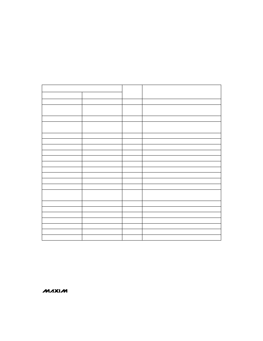
21
1, 4, 17, 25, 26, 38, 39
Negative Analog Supply (nominally -5.2V)
ECL Clock Input Pin
2, 19, 22, 24, 27, 28, 36,
37, 40, 42
No Connect. Not internally connected.
20
PIN
6, 15
Digital Ground
Inverse ECL Clock Input Pin
7
Digital Data Output (LSB)
--
--
Overrange Output
Reference Voltage Bottom, Sense
30, 34
14
Digital Data Output (MSB)
Analog Input. Can be connected to the input
signal or used as a sense.
8≠13
Digital Data Output
32
Reference Voltage Tap 2 (typically -1V)
--
Reference Voltage Top, Sense
41
Reference Voltage Top, Force
--
--
Data-Ready Output
Data-Ready Inverse
CLK
V
EE
N.C.
CLK
DGND
D0
VRBS
D8
VIN
D7
D1≠D6
VR2
VRTS
VRTF
DRINV
DREADY
6
3, 7, 12, 22, 27, 32
28, 30
5
1, 34
36
10
44
15, 19
43
37≠42
17
24
23
29
35
3
D0≠D6 Output Inversion Control
LINV
31
5, 16, 29, 31, 33, 35
Analog Ground
AGND
2, 8, 9, 14, 16, 18, 20,
25, 26, 33
23
Reference Voltage Bottom, Force
VRBF
11
--
Reference Voltage Tap 1 (typically -1.5V)
VR1
13
--
Reference Voltage Tap 3 (typically -0.5V)
VR3
21
______________________________________________________________Pin Description
FUNCTION
Ceramic SB
NAME
CERQUAD
The MAX1125 is a 300Msps, monolithic, 8-bit parallel
flash analog-to-digital converter (ADC) with an analog
bandwidth of over 200MHz. A major advance over pre-
vious flash converters is the inclusion of 256 input pre-
amplifiers between the reference ladder and input
comparators. (See
Functional Diagram.) This feature
not only reduces clock-transient kickback to the input
and reference ladder due to a low AC beta, but also
reduces the effect of the dynamic state of the input sig-
nal on the latching characteristics of the input compara-
tors. The preamplifiers act as buffers and stabilize the
input capacitance so it remains constant for varying
input voltages and frequencies, making the part easier
to drive than previous flash converters. The MAX1125
incorporates a special decoding scheme that reduces
metastable errors (sparkle codes or flyers) to a maxi-
mum of 1LSB.
_______________Detailed Description
18
D7 Output Inversion Control
MINV
4