 | –≠–ª–µ–∫—Ç—Ä–æ–Ω–Ω—ã–π –∫–æ–º–ø–æ–Ω–µ–Ω—Ç: MAX1127 | –°–∫–∞—á–∞—Ç—å:  PDF PDF  ZIP ZIP |

General Description
The MAX1127 quad, 12-bit analog-to-digital converter
(ADC) features fully differential inputs, a pipelined
architecture, and digital error correction. This ADC is
optimized for low-power, high-dynamic performance for
medical imaging, communications, and instrumentation
applications. The MAX1127 operates from a 1.7V to
1.9V single supply and consumes only 563mW while
delivering a 69.6dB signal-to-noise ratio (SNR) at a
19.3MHz input frequency. In addition to low operating
power, the MAX1127 features a 675µA power-down
mode for idle periods.
An internal 1.24V precision bandgap reference sets the
ADC's full-scale range. A flexible reference structure
allows the use of an external reference for applications
requiring increased accuracy or a different input volt-
age range.
A single-ended clock controls the conversion process.
An internal duty-cycle equalizer allows for wide varia-
tions in input-clock duty cycle. An on-chip phase-
locked loop (PLL) generates the high-speed serial
low-voltage differential signaling (LVDS) clock.
The MAX1127 provides serial LVDS outputs for data,
clock, and frame alignment signals. The output data is
presented in two's complement or binary format.
Refer to the MAX1126 data sheet for a pin-compatible
40Msps version of the MAX1127.
The MAX1127 is available in a small, 10mm x 10mm x
0.9mm, 68-pin QFN package with exposed paddle and
is specified for the extended industrial (-40∞C to +85∞C)
temperature range.
Applications
Ultrasound and Medical Imaging
Positron Emission Tomography (PET) Imaging
Multichannel Communication Systems
Instrumentation
Features
Four ADC Channels with Serial LVDS/SLVS
Outputs
Excellent Dynamic Performance
69.6dB SNR at f
IN
= 19.3MHz
92dBc SFDR at f
IN
= 19.3MHz
-87dB Channel Isolation
Ultra-Low Power
135mW per Channel (Normal Operation)
1.2mW Total (Shutdown Mode)
Accepts 20% to 80% Clock Duty Cycle
Self-Aligning Data-Clock to Data-Output Interface
Fully Differential Analog Inputs
Wide ±1.4V
P-P
Differential Input Voltage Range
Internal/External Reference Option
Test Mode for Digital Signal Integrity
LVDS Outputs Support Up to 30in FR-4 Backplane
Connections
Small, 68-Pin QFN with Exposed Paddle
Evaluation Kit Available (MAX1127EVKIT)
MAX1127
Quad, 12-Bit, 65Msps, 1.8V ADC with
Serial LVDS Outputs
________________________________________________________________
Maxim Integrated Products
1
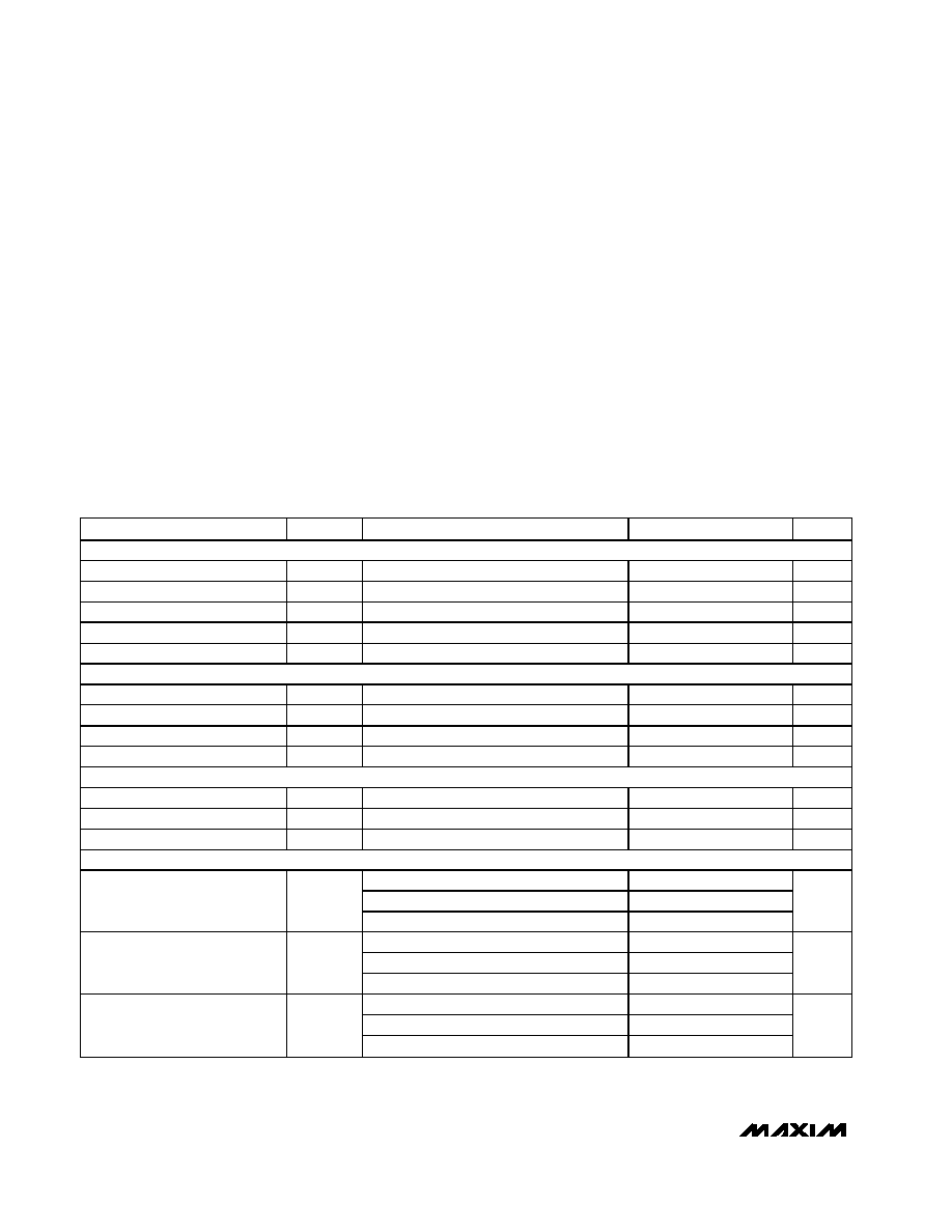
Ordering Information
19-3144; Rev 1; 3/04
For pricing, delivery, and ordering information, please contact Maxim/Dallas Direct! at
1-888-629-4642, or visit Maxim's website at www.maxim-ic.com.
PART
TEMP RANGE
PIN-PACKAGE
MAX1127EGK
-40∞C to +85∞C
68 QFN 10mm x
x 10mm x 0.9mm
35 OUT3N
36 OUT3P
37 OV
DD
38 OUT2N
39 OUT2P
40 OV
DD
41 FRAMEN
42 FRAMEP
43 OV
DD
44 CLKOUTN
45 CLKOUTP
46 OV
DD
47 OUT1N
48 OUT1P
49 OV
DD
50 OUT0N
51 OUT0P
52
OV
DD
53
PD0
54
PD1
55
PD2
56
PD3
57
PDALL
58
AV
DD
59
AV
DD
60
AV
DD
61
AV
DD
62
AV
DD
63
64
L
VDSTEST
65
GND
66
REFIO
67
68
GND
1
GND
2
IN0P
3
IN0N
4
GND
5
IN1P
6
IN1N
7
GND
8
AV
DD
9
AV
DD
10
AV
DD
11
GND
12
IN2P
13
IN2N
14
GND
15
IN3P
16
IN3N
17
GND
18
AV
DD
19
I.C.
20
AV
DD
21
CV
DD
22
GND
23
CLK
24
GND
25
AV
DD
26
AV
DD
27
AV
DD
28
DT
29
30
PLL0
31
PLL1
32
PLL2
33
PLL3
34
OV
DD
SL
VS/L
VDS
INTREF
T/B
MAX1127
QFN
10mm x 10mm x 0.9mm
EP
Pin Configuration
MAX1127
Quad, 12-Bit, 65Msps, 1.8V ADC with
Serial LVDS Outputs
2
_______________________________________________________________________________________
ABSOLUTE MAXIMUM RATINGS
ELECTRICAL CHARACTERISTICS
(AV
DD
= 1.8V, OV
DD
= 1.8V, CV
DD
= 1.8V, GND = 0, external V
REFIO
= 1.24V, INTREF = AV
DD
, C
REFIO
to GND = 0.1µF,
f
CLK
= 65MHz (50% duty cycle), DT = 0, T
A
= T
MIN
to T
MAX
, unless otherwise noted. Typical values are at T
A
= +25∞C.) (Note 1)
Stresses beyond those listed under "Absolute Maximum Ratings" may cause permanent damage to the device. These are stress ratings only, and functional
operation of the device at these or any other conditions beyond those indicated in the operational sections of the specifications is not implied. Exposure to
absolute maximum rating conditions for extended periods may affect device reliability.
AV
DD
to GND.........................................................-0.3V to +2.0V
CV
DD
to GND ........................................................-0.3V to +3.6V
OV
DD
to GND ........................................................-0.3V to +2.0V
IN_P, IN_N to GND...................................-0.3V to (AV
DD
+ 0.3V)
CLK to GND .............................................-0.3V to (CV
DD
+ 0.3V)
OUT_P, OUT_N, FRAME_,
CLKOUT_ to GND................................-0.3V to (OV
DD
+ 0.3V)
DT, SLVS/LVDS to GND ...........................-0.3V to (AV
DD
+ 0.3V)
PLL0, PLL1, PLL2, PLL3 to GND .............-0.3V to (AV
DD
+ 0.3V)
PD0, PD1, PD2, PD3, PDALL to GND......-0.3V to (AV
DD
+ 0.3V)
T/B, LVDSTEST to GND ...........................-0.3V to (AV
DD
+ 0.3V)
REFIO, INTREF to GND............................-0.3V to (AV
DD
+ 0.3V)
I.C. to GND...............................................-0.3V to (AV
DD
+ 0.3V)
Continuous Power Dissipation (T
A
= +70∞C)
68-Pin QFN 10mm x 10mm x 0.9mm
(derated 41.7mW/∞C above +70∞C)........................3333.3mW
Operating Temperature Range ...........................-40∞C to +85∞C
Maximum Junction Temperature .....................................+150∞C
Storage Temperature Range .............................-65∞C to +150∞C
Lead Temperature Range (soldering, 10s)......................+300∞C
PARAMETER
SYMBOL
CONDITIONS
MIN
TYP
MAX
UNITS
DC ACCURACY
Resolution
N
12
Bits
Integral Nonlinearity
INL
(Note 2)
±0.4
LSB
Differential Nonlinearity
DNL
(Note 2)
±0.25
LSB
Offset Error
Fixed external reference (Note 2)
±1
% FS
Gain Error
Fixed external reference (Note 2)
±1.5
% FS
ANALOG INPUTS (IN_P, IN_N)
Input Differential Range
V
ID
Differential input
1.4
V
P-P
Common-Mode Voltage Range
V
CMO
(Note 3)
0.75
V
Differential Input Impedance
R
IN
Switched capacitor load
2
k
Differential Input Capacitance
C
IN
12.5
pF
CONVERSION RATE
Maximum Conversion Rate
f
SMAX
65
MHz
Minimum Conversion Rate
f
SMIN
16
MHz
Data Latency
6.5
Cycles
DYNAMIC CHARACTERISTICS (differential inputs, 4096-point FFT)
f
IN
= 5.3MHz at -0.5dBFS
69.7
f
IN
= 19.3MHz at -0.5dBFS, T
A
+25∞C
66.6
69.6
Signal-to-Noise Ratio (Note 2)
SNR
f
IN
= 30.3MHz at -0.5dBFS
69.4
dB
f
IN
= 5.3MHz at -0.5dBFS
69.6
f
IN
= 19.3MHz at -0.5dBFS, T
A
+25∞C
66.5
69.5
Signal-to-Noise and Distortion
(First Four Harmonics) (Note 2)
SINAD
f
IN
= 30.3MHz at -0.5dBFS
69.3
dB
f
IN
= 5.3MHz at -0.5dBFS
11.4
f
IN
= 19.3MHz at -0.5dBFS, T
A
+25∞C
11.4
Effective Number of Bits (Note 2)
ENOB
f
IN
= 30.3MHz at -0.5dBFS
11.3
Bits

MAX1127
Quad, 12-Bit, 65Msps, 1.8V ADC with
Serial LVDS Outputs
_______________________________________________________________________________________
3
ELECTRICAL CHARACTERISTICS (continued)
(AV
DD
= 1.8V, OV
DD
= 1.8V, CV
DD
= 1.8V, GND = 0, external V
REFIO
= 1.24V, INTREF = AV
DD
, C
REFIO
to GND = 0.1µF,
f
CLK
= 65MHz (50% duty cycle), DT = 0, T
A
= T
MIN
to T
MAX
, unless otherwise noted. Typical values are at T
A
= +25∞C.) (Note 1)
PARAMETER
SYMBOL
CONDITIONS
MIN
TYP
MAX
UNITS
f
IN
= 5.3MHz at -0.5dBFS
93.3
f
IN
= 19.3MHz at -0.5dBFS, T
A
+25∞C
77.5
92
Spurious-Free Dynamic Range
(Note 2)
SFDR
f
IN
= 30.3MHz at -0.5dBFS
88.9
dBc
f
IN
= 5.3MHz at -0.5dBFS
-91
f
IN
= 19.3MHz at -0.5dBFS, T
A
+25∞C
-91
-77.5
Total H ar m oni c D i stor ti on ( N ote 2)
THD
f
IN
= 30.3MHz at -0.5dBFS
-88
dBc
Inter m od ul ati on D i stor ti on
IMD
f
1
= 12.348685MHz at -6.5dBFS,
f
2
= 13.650845MHz at -6.5dBFS ( N ote 2)
91.2
dBc
Third-Order Intermodulation
IM3
(Note 2)
95.7
dBc
Aperture Jitter
t
AJ
(Note 2)
<0.4
ps
RMS
Aperture Delay
t
AD
(Note 2)
1
ns
Small-Signal Bandwidth
SSBW
Input at -20dBFS (Notes 2 and 4)
100
MHz
Full-Power Bandwidth
LSBW
Input at -0.5dBFS (Notes 2 and 4)
100
MHz
Output Noise
INP = IN_N
0.35
LSB
RMS
Overdrive Recovery Time
t
OR
R
S
= 25, C
S
= 50pF
1
Clock
cycles
INTERNAL REFERENCE (
INTREF
= GND, bypass REFIO to GND with 0.1µF)
INTREF Internal Reference Mode
Enable Voltage
(Note 5)
0.1
V
INTREF Low-Leakage Current
200
µA
REFIO Output Voltage
V
REFIO
1.18
1.24
1.30
V
Reference Temperature
Coefficient
TC
REFIO
100
ppm/∞C
EXTERNAL REFERENCE (
INTREF
= AV
DD
)
INTREF External Reference Mode
Enable Voltage
(Note 5)
AV
DD
-
0.1V
V
INTREF High-Leakage Current
200
µA
REFIO Input Voltage Range
1.24
V
REFIO Input Current
I
REFIO
<1
µA
CLOCK INPUT (CLK)
Input High Voltage
V
CLKH
0.8 x
CV
DD
V
Input Low Voltage
V
CLKL
0.2 x
CV
DD
V
Clock Duty Cycle
50
%
Clock Duty-Cycle Tolerance
±30
%

MAX1127
Quad, 12-Bit, 65Msps, 1.8V ADC with
Serial LVDS Outputs
4
_______________________________________________________________________________________
ELECTRICAL CHARACTERISTICS (continued)
(AV
DD
= 1.8V, OV
DD
= 1.8V, CV
DD
= 1.8V, GND = 0, external V
REFIO
= 1.24V, INTREF = AV
DD
, C
REFIO
to GND = 0.1µF,
f
CLK
= 65MHz (50% duty cycle), DT = 0, T
A
= T
MIN
to T
MAX
, unless otherwise noted. Typical values are at T
A
= +25∞C.) (Note 1)
PARAMETER
SYMBOL
CONDITIONS
MIN
TYP
MAX
UNITS
Input at GND
5
Input Leakage
DI
IN
Input at AV
DD
80
µA
Input Capacitance
DC
IN
5
pF
DIGITAL INPUTS (PLL_, LVDSTEST, DT, SLVS/
LVDS
, PD_, PDALL,
T
/B)
Input High Threshold
V
IH
0.8 x
AV
DD
V
Input Low Threshold
V
IL
0.2 x
AV
DD
V
Input at GND, except PLL2 and PLL3
5
Input at AV
DD
, except PLL2 and PLL3
80
Input Leakage
DI
IN
PLL2 and PLL3 only
200
µA
Input Capacitance
DC
IN
5
pF
LVDS OUTPUTS (OUT_P, OUT_N, SLVS/
LVDS
= 0)
Differential Output Voltage
V
OHDIFF
R
TERM
= 100
250
450
mV
Output Common-Mode Voltage
V
OCM
R
TERM
= 100
1.125
1.375
V
Rise Time (20% to 80%)
t
R
R
TERM
= 100, C
LOAD
= 5pF
150
ps
Fall Time (80% to 20%)
t
F
R
TERM
= 100, C
LOAD
= 5pF
150
ps
SLVS OUTPUTS (OUT_P, OUT_N, CLKOUTP, CLKOUTN, FRAMEP, FRAMEN), SLVS/
LVDS
= 1, DT = 1
Differential Output Voltage
V
OHDIFF
R
TERM
= 100
240
mV
Output Common-Mode Voltage
V
OCM
R
TERM
= 100
220
mV
Rise Time (20% to 80%)
t
R
R
TERM
= 100, C
LOAD
= 5pF
120
ps
Fall Time (80% to 20%)
t
F
R
TERM
= 100, C
LOAD
= 5pF
120
ps
POWER-DOWN
PD Fall to Output Enable
t
ENABLE
132
µs
PD Rise to Output Disable
t
DISABLE
10
ns
POWER REQUIREMENTS
AV
DD
Supply Voltage
AV
DD
1.7
1.8
1.9
V
OV
DD
Supply Voltage
OV
DD
1.7
1.8
1.9
V
CV
DD
Supply Voltage
CV
DD
1.7
1.8
3.6
V
MAX1127
Quad, 12-Bit, 65Msps, 1.8V ADC with
Serial LVDS Outputs
_______________________________________________________________________________________
5
ELECTRICAL CHARACTERISTICS (continued)
(AV
DD
= 1.8V, OV
DD
= 1.8V, CV
DD
= 1.8V, GND = 0, external V
REFIO
= 1.24V, INTREF = AV
DD
, C
REFIO
to GND = 0.1µF,
f
CLK
= 65MHz (50% duty cycle), DT = 0, T
A
= T
MIN
to T
MAX
, unless otherwise noted. Typical values are at T
A
= +25∞C.) (Note 1)
PARAMETER
SYMBOL
CONDITIONS
MIN
TYP
MAX
UNITS
PDALL = 0, all channels
active
257
295
PDALL = 0, all channels
active, DT = 1
257
PDALL = 0, 1 channel active
82
PDALL = 0, PD[3:0] = 1111
23
mA
AV
DD
Supply Current
I
AVDD
f
IN
=
19.3MHz at
-0.5dBFS
PDALL = 1, global power
down, PD[3:0] =1111, no
clock input
300
µA
PDALL = 0, all channels
active
56
65
PDALL = 0, all channels
active, DT = 1
72
PDALL = 0, 1 channel active
42
PDALL = 0, PD[3:0] = 1111
37
mA
OV
DD
Supply Current
I
OVDD
f
IN
=
19.3MHz at
-0.5dBFS
PDALL = 1, global power-
down, PD[3:0] =1111, no
clock input
375
µA
CV
DD
Supply Current
I
CVDD
CV
DD
is used only to bias ESD-protection
diodes on CLK input, Figure 2
0
mA
Power Dissipation
P
DISS
f
IN
= 19.3MHz at -0.5dBFS
563
648
mW
TIMING CHARACTERISTICS
(Note 6)
Data Valid to CLKOUT Rise/Fall
t
OD
f
CLK
= 65MHz, Figure 5 (Notes 6 and 7)
(t
SAMPLE
/
24)
- 0.15
t
SAMPLE
/
24
(t
SAMPLE
/
24)
+ 0.15
ns
CLKOUT Output Width High
t
CH
Figure 5
t
S AMP LE
/
12
ns
CLKOUT Output Width Low
t
CL
Figure 5
t
S AMP LE
/
12
ns
FRAME Rise to CLKOUT Rise
t
CF
Figure 4 (Note 7)
(t
SAMPLE
/
24)
- 0.15
t
SAMPLE
/
24
( t
SAMPLE
/
24)
+ 0.15
ns
Sample CLK Rise to Frame Rise
t
SF
Figure 4 (Notes 7 and 8)
(t
SAMPLE
/
2)
+0.9
(t
SAMPLE
/
2)
+1.3
(t
SAMPLE
/
2)
+1.7
ns