Äîêóìåíòàöèÿ è îïèñàíèÿ www.docs.chipfind.ru
General Description
The MAX1144/MAX1145 are 150ksps, 14-bit ADCs.
These serially interfaced ADCs connect directly to
SPITM, QSPITM, and MICROWIRETM devices without
external logic. They combine an input scaling network,
internal track/hold, clock, and three general-purpose
digital output pins (for external multiplexer or PGA con-
trol) in a 20-pin SSOP package. The excellent dynamic
performance (THD
90dB), high speed (150ksps in
bipolar mode), and low power (8.0mA) of these ADCs
make them ideal for applications such as industrial
process control, instrumentation, and medical applica-
tions.
The MAX1144 accepts input signals of 0 to +6V (unipo-
lar) or ±6V (bipolar), while the MAX1145 accepts input
signals of 0 to +2.048V (unipolar) or ±2.048V (bipolar).
Operating from a single 3.135V to 3.465V analog digital
supply, powerdown modes reduce current consump-
tion to 0.15mA at 10ksps and further reduce supply
current to less than 20µA slower data rates.
A serial strobe output (SSTRB) allows direct connection
to the TMS320 family digital-signal processors. The
MAX1144/MAX1145 user can select either the internal
clock or an external serial-interface clock for the ADC to
perform analog-to-digital conversions.
The MAX1144/MAX1145 feature internal calibration cir-
cuitry to correct linearity and offset errors. On-demand
calibration allows the user to optimize performance.
Three user-programmable logic outputs are provided
for the control of an 8-channel mux or PGA.
The MAX1144/MAX1145 are available in a 20-pin SSOP
package and are fully specified over the -40°C to
+85°C temperature range.
Applications
Industrial Process Control
Industrial I/O Modules
Data-Acquisition Systems
Medical Instruments
Portable and Battery-Powered Equipment
Features
o 150ksps (Bipolar) and 125ksps (Unipolar)
Sampling ADC
o 14 Bits, No Missing Codes
o 1LSB INL Guaranteed
o -100dB THD
o 3.3V Single-Supply Operation
o Low-Power Operation
5mA typ (Unipolar Mode)
o 1.2µA Shutdown Mode
o Software-Configurable Unipolar and Bipolar Input
Ranges
0 to +6V and ±6V (MAX1144)
0 to +2.048V and ±2.048V (MAX1145)
o Internal or External Clock
o SPI/QSPI/MICROWIRE TMS320-Compatible Serial
Interface
o Three User-Programmable Logic Outputs
o Small 20-Pin SSOP Package
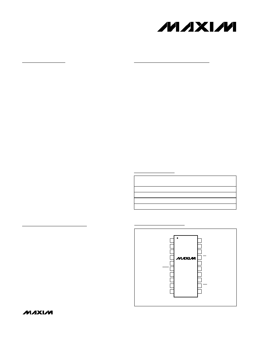
MAX1144/MAX1145
14-Bit ADCs, 150ksps, 3.3V Single Supply
________________________________________________________________ Maxim Integrated Products
1
20
19
18
17
16
15
14
13
1
2
3
4
5
6
7
8
AIN
AGND
CREF
CS
AV
DD
AGND
AV
DD
REF
TOP VIEW
DIN
DV
DD
DGND
SCLK
P1
P2
SHDN
DGND
12
11
9
10
RST
DOUT
SSTRB
PO
MAX1144
MAX1145
SSOP
Pin Configuration
Ordering Information
19-2465; Rev 0; 4/02
For pricing, delivery, and ordering information, please contact Maxim/Dallas Direct! at
1-888-629-4642, or visit Maxim's website at www.maxim-ic.com.
Ordering Information continued at end of data sheet.
Functional Diagram and Typical Application Circuit appear
at end of data sheet.
PART
TEMP
RANGE
PIN-
PACKAGE
INL
(LSB)
MAX1144ACAP
0
°C to +70°C
20 SSOP
±1
MAX1144BCAP
0
°C to +70°C
20 SSOP
±2
MAX1144AEAP
-40
°C to +85°C
20 SSOP
±1
MAX1144BEAP
-40
°C to +85°C
20 SSOP
±2
SPI and QSPI are trademarks of Motorola, Inc.
MICROWIRE is a trademark of National Semiconductor, Corp.
MAX1144/MAX1145
14-Bit ADCs, 150ksps, 3.3V Single Supply
2
_______________________________________________________________________________________
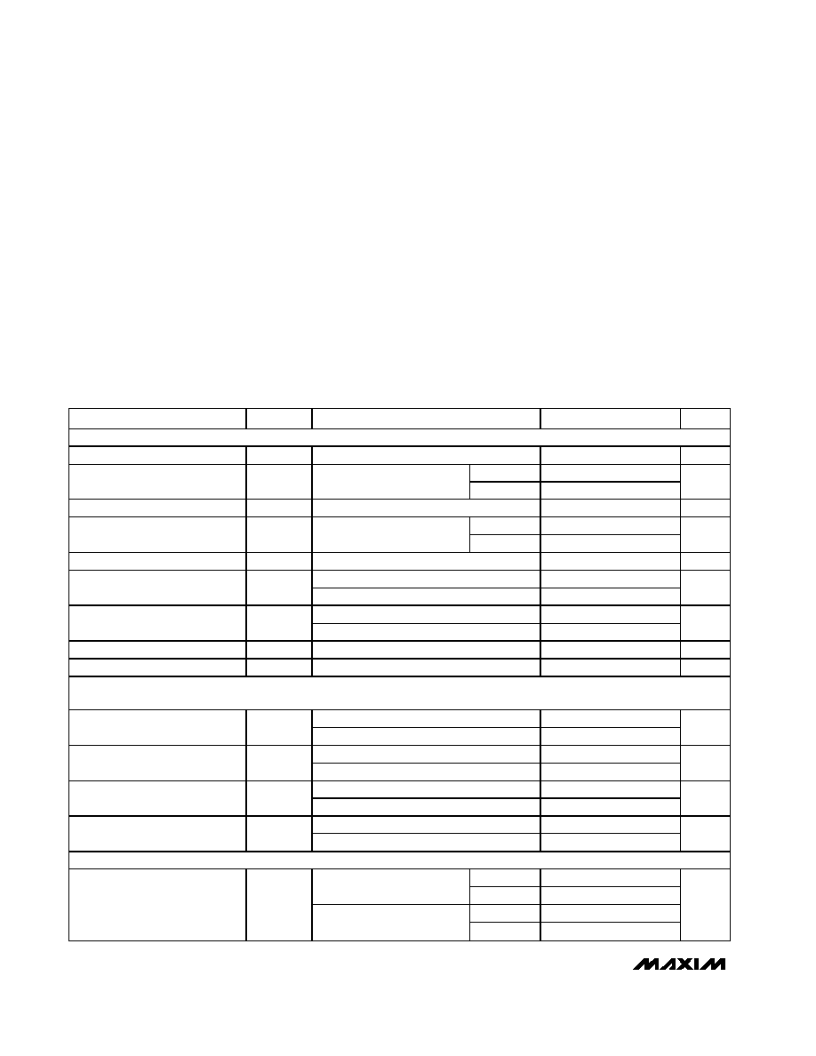
ABSOLUTE MAXIMUM RATINGS
ELECTRICAL CHARACTERISTICS
(AV
DD
= DV
DD
= 3.3V ±5%, f
SCLK
= 3.6MHz, external clock (50% duty cycle), 24 clocks/conversion (150ksps), bipolar input, V
REF
=
2.048V, C
REF
= 4.7µF, C
CREF
= 1µF, T
A
= T
MIN
to T
MAX
, unless otherwise noted. Typical values are at T
A
= +25°C.)
Stresses beyond those listed under "Absolute Maximum Ratings" may cause permanent damage to the device. These are stress ratings only, and functional
operation of the device at these or any other conditions beyond those indicated in the operational sections of the specifications is not implied. Exposure to
absolute maximum rating conditions for extended periods may affect device reliability.
AV
DD
to AGND, DV
DD
to DGND ..............................-0.3V to +6V
AGND to DGND.....................................................-0.3V to +0.3V
AIN to AGND ....................................................................±16.5V
CREF, REF to AGND ................................-0.3V to (AV
DD
+ 0.3V)
Digital Inputs to DGND.............................................-0.3V to +6V
Digital Outputs to DGND .........................-0.3V to (DV
DD
+ 0.3V)
Continuous Power Dissipation (T
A
= +70°C)
20-Pin SSOP (derate 8.00mW/°C above +70°C) .........640mW
Operating Temperature Ranges
MAX114_ _CAP...................................................0°C to +70°C
MAX114_ _EAP ................................................-40°C to +85°C
Storage Temperature Range .............................-60°C to +150°C
Junction Temperature ......................................................+150°C
Lead Temperature (soldering, 10s) .................................+300°C
PARAMETER
SYMBOL
CONDITIONS
MIN
TYP
MAX
UNITS
DC ACCURACY (Note 1)
Resolution
14
Bits
MAX114_A
±1
Relative Accuracy
INL
Bipolar mode (Note 2)
MAX114_B
±2
LSB
No Missing Codes
14
Bits
MAX114_A
-1
+1
Differential Nonlinearity
DNL
Bipolar mode
MAX114_B
-1.00
+1.75
LSB
Transition Noise
0.47
LSB
RMS
Unipolar
±4
Offset Error
Bipolar
±6
mV
Unipolar
±0.2
Gain Error (Note 3)
Bipolar
±0.3
%FSR
Offset Drift (Bipolar and Unipolar)
Excluding reference drift
±1
ppm/°C
Gain Drift (Bipolar and Unipolar)
Excluding reference drift
±4
ppm/°C
D YNA M IC SPEC IF IC A T IO N S ( 5 k Hz SINE- WAVE IN PU T, 1 50 k s ps , 3 .6M H Z C L O CK , BIPO LA R IN PU T M O DE. M A X1 14 4 , 1 2 V
P-P
. M A X1 14 5 ,
4 .09 6 V
P-P
.)
f
IN
= 5kHz
78
82
Signal-to-Noise Plus Distortion
(SINAD)
f
IN
= 75kHz
81
dB
f
IN
= 5kHz
78
82
Signal-to-Noise Ratio
(SNR)
f
IN
= 75kHz
81
dB
f
IN
= 5kHz
-100
-90
Total Harmonic Distortion
(THD)
f
IN
= 75kHz
-94
dB
f
IN
= 5kHz
92
105
Spurious-Free-Dynamic Range
(SFDR)
f
IN
= 75kHz
98
dB
ANALOG INPUT
Unipolar
0
+6
MAX1144
Bipolar
-6
+6
Unipolar
0
+2.048
Input Range
MAX1145
Bipolar
-2.048
+2.048
V
MAX1144/MAX1145
14-Bit ADCs, 150ksps, 3.3V Single Supply
_______________________________________________________________________________________
3
ELECTRICAL CHARACTERISTICS (continued)
(AV
DD
= DV
DD
= 3.3V ±5%, f
SCLK
= 3.6MHz, external clock (50% duty cycle), 24 clocks/conversion (150ksps), bipolar input, V
REF
=
2.048V, C
REF
= 4.7µF, C
CREF
= 1µF, T
A
= T
MIN
to T
MAX
, unless otherwise noted. Typical values are at T
A
= +25°C.)
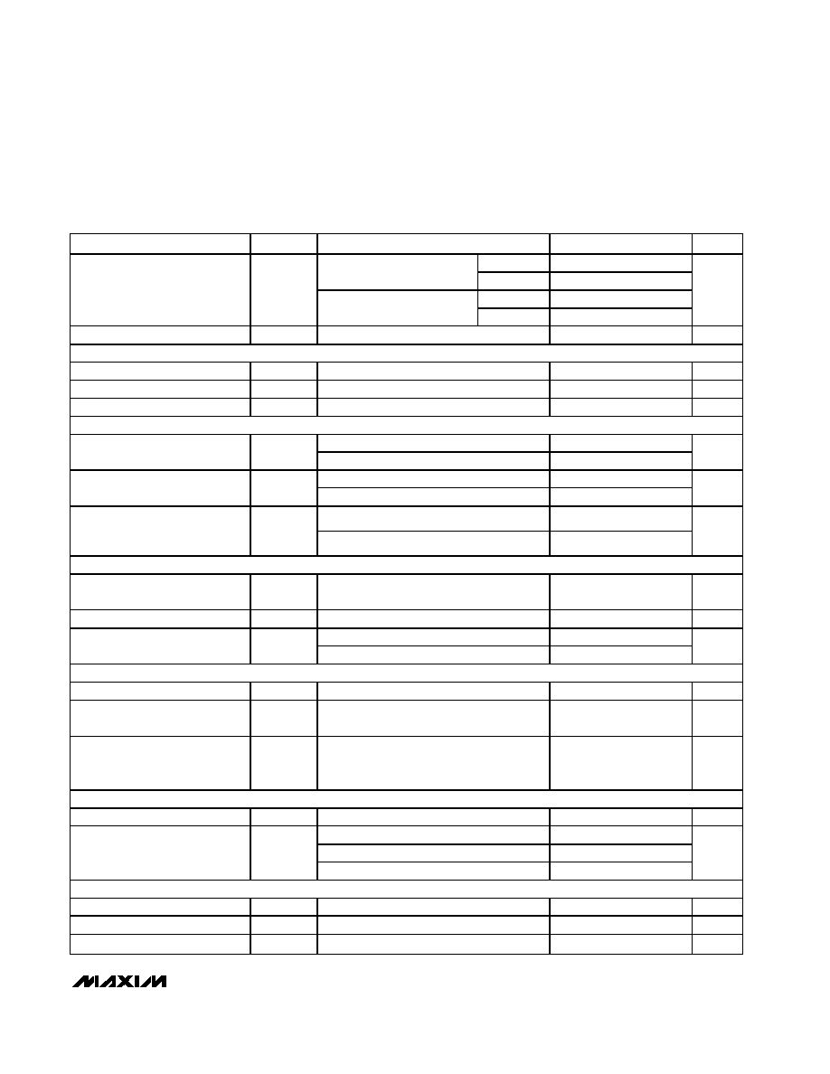
PARAMETER
SYMBOL
CONDITIONS
MIN
TYP
MAX
UNITS
Unipolar
7.5
10.5
MAX1144
Bipolar
5.9
8.4
Unipolar
100
1000
Input Impedance
MAX1145
Bipolar
3.4
5.3
k
Input Capacitance
32
pF
CONVERSION RATE
Internal Clock Frequency
3
MHz
Aperture Delay
t
AD
10
ns
Aperture Jitter
t
AJ
50
ps
MODE 1 (24 EXTERNAL CLOCK CYCLES PER CONVERSION)
Unipolar
0.1
3.0
External Clock Frequency
f
SCLK
Bipolar
0.1
3.6
MHz
Unipolar
4.17
125
Sample Rate
f
S
=
f
SCLK
/ 24
Bipolar
4.17
150
ksps
Unipolar
8
240
Conversion Time (Note 4)
t
CONV+ACQ
= 24 / f
SCLK
Bipolar
6.7
240
µs
MODE 2 (INTERNAL CLOCK)
External Clock Frequency
(Data Transfer Only)
4
MHz
Conversion Time
(SSTRB low pulse width)
5.3
7
µs
Unipolar
1.67
Acquisition Time (Note 5)
Bipolar
1.39
µs
MODE 3 (32 EXTERNAL CLOCK CYCLES PER CONVERSION)
External Clock Frequency
f
SCLK
Unipolar or bipolar
0.1
3.6
MHz
Sample Rate
f
S
=
f
SCLK
/ 32
Unipolar or bipolar
3.125
112
ksps
Conversion Time (Note 4)
t
CONV+ACQ
= 32 / f
SCLK
Unipolar or bipolar
8.89
320
µs
EXTERNAL REFERENCE
Input Range
(Notes 6, 7)
1.9
2.048
2.2
V
V
REF
= 2.048V, f
SCLK
= 3.6MHz
110
V
REF
= 2.048V, f
SCLK
= 0
100
Input Current
In power-down, f
SCLK
= 0
0.1
µA
DIGITAL INPUTS
Input High Voltage
V
IH
2.4
V
Input Low Voltage
V
IL
0.8
V
Input Leakage
I
IN
V
IN
= 0 or DV
DD
-1
+1
µA
MAX1144/MAX1145
14-Bit ADCs, 150ksps, 3.3V Single Supply
4
_______________________________________________________________________________________
PARAMETER
SYMBOL
CONDITIONS
MIN
TYP
MAX
UNITS
Input Hysteresis
V
HYST
0.2
V
Input Capacitance
C
IN
10
pF
DIGITAL OUTPUTS
Output High Voltage
V
OH
I
SOURCE
= 0.5mA
DV
DD
-
0.5
V
I
SINK
= 5mA
0.4
Output Low Voltage
V
OL
I
SINK
= 16mA
0.8
V
Three-State Leakage Current
I
L
CS = DV
DD
-10
+10
µA
Three-State Output Capacitance
CS = DV
DD
10
pF
POWER SUPPLIES
Analog Supply
AV
DD
3.135
3.3
3.465
V
Digital Supply
DV
DD
3.135
3.3
3.465
V
Unipolar mode
3.9
8
Bipolar mode
7
11
mA
Analog Supply Current
I
ANALOG
SHDN = 0, or software power-down mode
0.1
10
µA
Unipolar or bipolar mode
1
2
mA
Digital Supply Current
I
DIGITAL
SHDN = 0, or software power-down mode
1.1
10
µA
Power-Supply Rejection Ratio
(Note 8)
PSRR
AV
DD
= DV
DD
= 3.135V to 3.465V
65
dB
ELECTRICAL CHARACTERISTICS (continued)
(AV
DD
= DV
DD
= 3.3V ±5%, f
SCLK
= 3.6MHz, external clock (50% duty cycle), 24 clocks/conversion (150ksps), bipolar input, V
REF
=
2.048V, C
REF
= 4.7µF, C
CREF
= 1µF, T
A
= T
MIN
to T
MAX
, unless otherwise noted. Typical values are at T
A
= +25°C.)
TIMING CHARACTERISTICS (Figures 5 and 6)
(AV
DD
= DV
DD
= 3.3V ±5%, T
A
= T
MIN
to T
MAX
, unless otherwise noted.)
PARAMETER
SYMBOL
CONDITIONS
MIN
TYP
MAX
UNITS
DIN to SCLK Setup
t
DS
50
ns
DIN to SCLK Hold
t
DH
0
ns
SCLK to DOUT Valid
t
DO
70
ns
CS Fall to DOUT Enable
t
DV
C
LOAD
= 50pF
80
ns
CS Rise to DOUT Disable
t
TR
C
LOAD
= 50pF
80
ns
CS to SCLK Rise Setup
t
CSS
100
ns
CS to SCLK Rise Hold
t
CSH
0
ns
SCLK High Pulse Width
t
CH
120
ns
SCLK Low Pulse Width
t
CL
120
ns
SCLK Fall to SSTRB
t
SSTRB
C
LOAD
= 50pF
80
ns
CS Fall to SSTRB Enable
t
SDV
C
LOAD
= 50pF, external clock mode
80
ns
CS Rise to SSTRB Disable
t
STR
C
LOAD
= 50pF, external clock mode
80
ns
SSTRB Rise to SCLK Rise
t
SCK
Internal clock mode
0
ns
RST Pulse Width
t
RS
278
70
ns
MAX1144/MAX1145
14-Bit ADCs, 150ksps, 3.3V Single Supply
_______________________________________________________________________________________
5
TIMING CHARACTERISTICS (Figures 5 and 6) (continued)
(AV
DD
= DV
DD
= 3.3V ±5%, T
A
= T
MIN
to T
MAX
, unless otherwise noted.)
Note 1: Tested at AV
DD
= DV
DD
= 3.3V, bipolar input mode.
Note 2: Relative accuracy is the deviation of the analog value at any code from its theoretical value after the gain error and offset
error have been nullified.
Note 3: Offset nullified.
Note 4: Conversion time is defined as the number of clock cycles multiplied by the clock period; clock has 50% duty cycle. Includes
the acquisition time.
Note 5: Acquisition time is 5 clock cycles in short acquisition mode and 13 clock cycles in long acquisition mode.
Note 6: Performance is limited by the converter's noise floor, typically 300µV
P-P
.
Note 7: When an external reference has a different voltage than the specified typical value, the full scale of the ADC scales propor-
tionally.
Note 8: Defined as the change in positive full scale caused by a ±5% variation in the nominal supply voltage.
Typical Operating Characteristics
(MAX1144/MAX1145, AV
DD
= DV
DD
= 3.3V, f
SCLK
= 3.6MHz, external clock (50% duty cycle), 24 clocks/conversion (150ksps),
bipolar input, REF = 2.048V, 4.7µF on REF, 1µF on CREF, T
A
= +25°C, unless otherwise noted.)
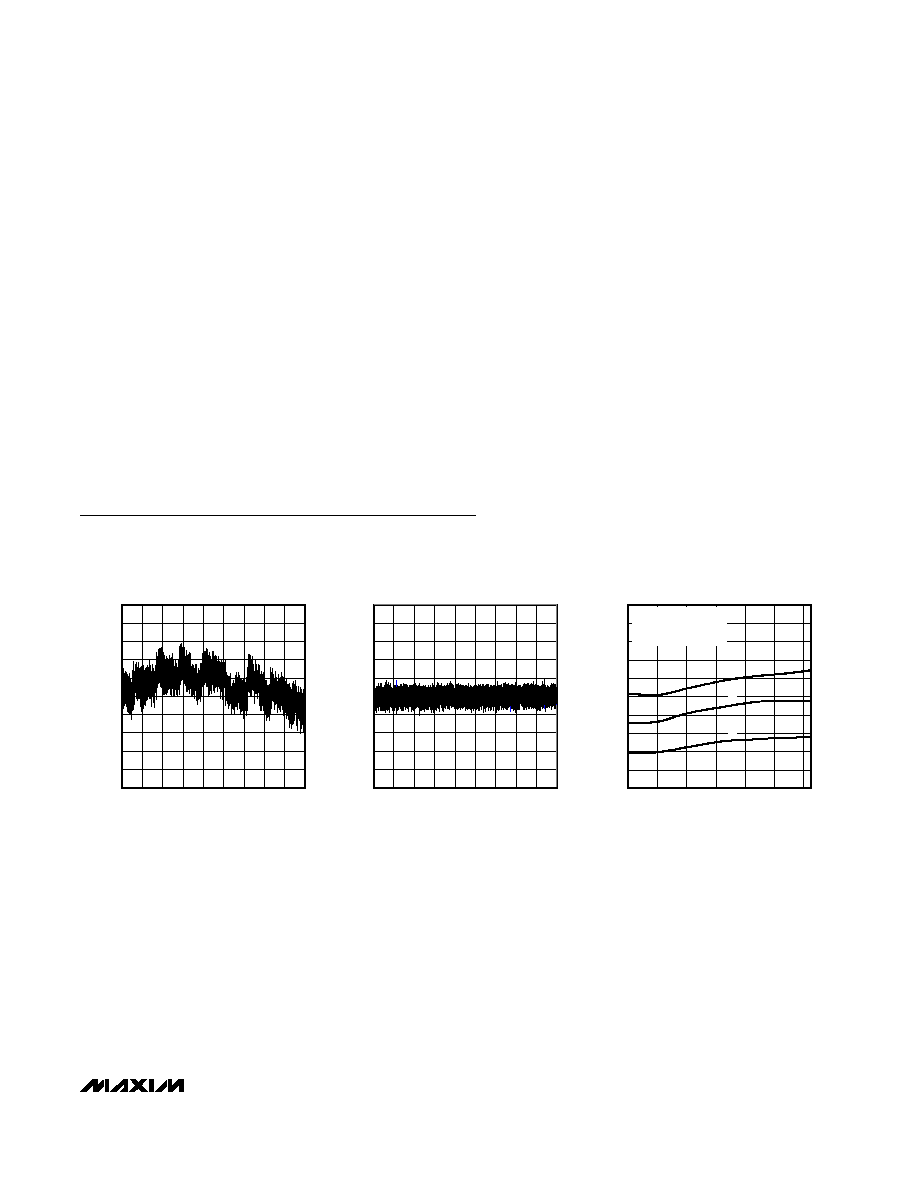
INTEGRAL NONLINEARITY
vs. DIGITAL OUTPUT CODE
MAX1144/45 toc01
DIGITAL OUTPUT CODE
INTEGRAL NONLINEARITY (LSB)
13649
11943
8531
10237
3413
5119
6825
1707
-0.8
-0.6
-0.4
-0.2
0
0.2
0.4
0.6
0.8
1.0
-1.0
1
15355
DIFFERENTIAL NONLINEARITY
vs. DIGITAL OUTPUT CODE
MAX1144/45 toc02
DIGITAL OUTPUT CODE
DIFFERENTIAL NONLINEARITY (LSB)
13649
11943
8531
10237
3413
5119
6825
1707
-0.8
-0.6
-0.4
-0.2
0
0.2
0.4
0.6
0.8
1.0
-1.0
1
15355
TOTAL SUPPLY CURRENT
vs. TEMPERATURE
MAX1144/45 toc03
TEMPERATURE (
°C)
TOTAL SUPPLY CURRENT (mA)
80
60
20
40
0
-20
8.1
8.2
8.3
8.4
8.5
8.6
8.7
8.8
8.9
9.0
8.0
-40
A: AV
DD
, DV
DD
= 3.135V
B: AV
DD
, DV
DD
= 3.3V
C: AV
DD
, DV
DD
= 3.465V
C
B
A