 | ÐлекÑÑоннÑй компоненÑ: MAX1154 | СкаÑаÑÑ:  PDF PDF  ZIP ZIP |
MAX1153 DS
General Description
The MAX1153/MAX1154 are stand-alone, 10-channel (8
external, 2 internal) 10-bit system monitor ADCs with
internal reference. A programmable single-ended/dif-
ferential mux accepts voltage and remote-diode tem-
perature-sensor inputs. These devices independently
monitor the input channels without microprocessor
interaction and generate an interrupt when any variable
exceeds user-defined limits. The MAX1153/MAX1154
configure both high and low limits, as well as the num-
ber of fault cycles allowed, before generating an inter-
rupt. These ADCs can also perform recursive data
averaging for noise reduction. Programmable wait inter-
vals between conversion sequences allow the selection
of the sample rate.
At the maximum sampling rate of 94ksps (auto mode,
single channel enabled), the MAX1153 consumes only
5mW (1.7mA at 3V). AutoShutdown
TM
reduces supply
current to 190µA at 2ksps and to less than 8µA at 50sps.
Stand-alone operation, combined with ease of use in a
small package (16-pin TSSOP), makes the MAX1153/
MAX1154 ideal for multichannel system-monitoring
applications. Low power consumption also makes
these devices a good fit for hand-held and battery-pow-
ered applications.
Applications
System Supervision
Remote Telecom Networks
Server Farms
Remote Data Loggers
Features
o Monitor 10 Signals Without Processor
Intervention
o Eight External Channels Programmable as
Temperature or Voltage Monitors
o Intelligent Circuitry for Reliable Autonomous
Measurement
Programmable Digital Averaging Filter
Programmable Fault Counter
o Precision Measurements
10-Bit Resolution
±0.5 LSB INL, ±0.5 LSB DNL
±0.75°C Temperature Accuracy (typ)
o Flexible
Automatic Channel Scan Sequencer with
Programmable Intervals
Programmable Inputs: Single Ended/Differential,
Voltage/Temperature
Programmable Wait State
o Internal 2.5V/4.096V Reference
(MAX1153/MAX1154)
o Remote Temperature Sensing Up to 10m
(Differential Mode)
o Single 3V or 5V Supply Operation
o Small 16-Pin TSSOP Package
MAX1153/MAX1154
Stand-Alone, 10-Channel, 10-Bit System Monitors
with Internal Temperature Sensor and V
DD
Monitor
________________________________________________________________ Maxim Integrated Products
1
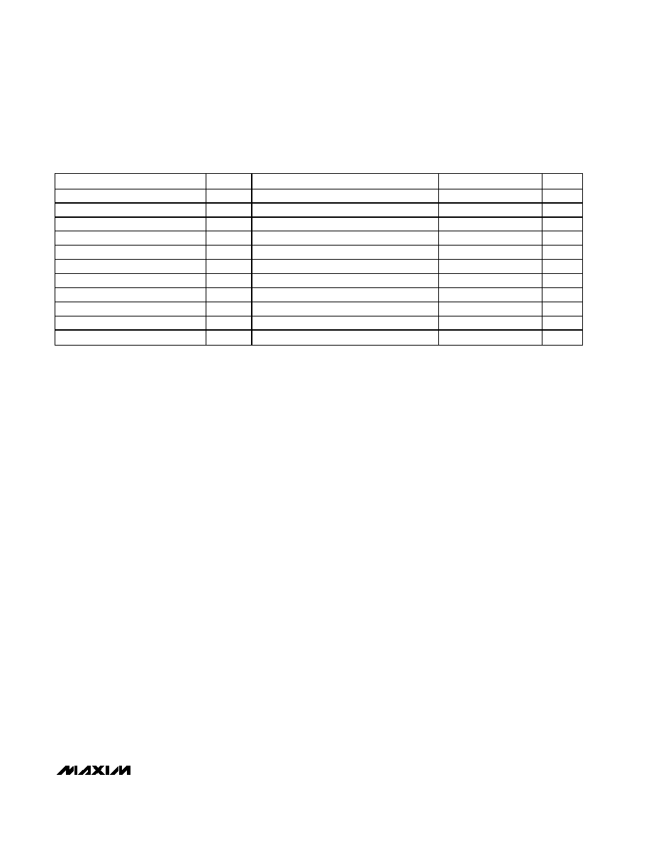
Selector Guide
19-2839; Rev 0; 4/03
For pricing, delivery, and ordering information, please contact Maxim/Dallas Direct! at
1-888-629-4642, or visit Maxim's website at www.maxim-ic.com.
Typical Application Circuit appears at end of data sheet.
AutoShutdown is a trademark of Maxim Integrated Products, Inc.
PART
INL (LSB)
TEMP
ERROR (°C)
SUPPLY
VOLTAGE (V)
MAX1153AEUE*
±0.5
±1.0
2.7 to 3.6
MAX1153BEUE
±0.5
±3.0
2.7 to 3.6
MAX1154AEUE*
±0.5
±1.0
4.5 to 5.5
MAX1154BEUE
±0.5
±2.5
4.5 to 5.5
16
15
14
13
12
11
10
9
1
2
3
4
5
6
7
8
AIN0
SCLK
CS
DIN
V
DD
GND
DOUT
INT
REF
TOP VIEW
MAX1153
MAX1154
TSSOP
AIN1
AIN2
AIN5
AIN3
AIN4
AIN6
AIN7
Pin Configuration
Ordering Information
PART
TEMP RANGE
PIN-PACKAGE
MAX1153AEUE*
-40°C to +85°C
16 TSSOP
MAX1153BEUE
-40°C to +85°C
16 TSSOP
MAX1154AEUE*
-40°C to +85°C
16 TSSOP
MAX1154BEUE
-40°C to +85°C
16 TSSOP
*Future product--contact factory for availability.
*Future product--contact factory for availability.
MAX1153/MAX1154
Stand-Alone, 10-Channel, 10-Bit System Monitors
with Internal Temperature Sensor and V
DD
Monitor
2
_______________________________________________________________________________________
ABSOLUTE MAXIMUM RATINGS
Stresses beyond those listed under "Absolute Maximum Ratings" may cause permanent damage to the device. These are stress ratings only, and functional
operation of the device at these or any other conditions beyond those indicated in the operational sections of the specifications is not implied. Exposure to
absolute maximum rating conditions for extended periods may affect device reliability.
VDD to GND .............................................................-0.3V to +6V
Analog Inputs to GND (AIN0AIN7, REF) ... -0.3V to (V
DD
+ 0.3V)
Digital Inputs to GND (DIN, SCLK, CS) .... -0.3V to (V
DD
+ 0.3V)
Digital Outputs to GND (DOUT, INT) ........ -0.3V to (V
DD
+ 0.3V)
Digital Outputs Sink Current ............................................. 25mA
Maximum Current into Any Pin .......................................... 50mA
Continuous Power Dissipation (TA = +70°C)
16-Pin TSSOP (derate 8.7mW/°C above +70°C) .........696mW
Operating Temperature Range ...........................-40°C to +85°C
Junction Temperature ......................................................+150°C
Storage Temperature Range .............................-65°C to +150°C
Lead Temperature (soldering, 10s) .................................+300°C
PARAMETER
SYMBOL
CONDITIONS
MIN
TYP
MAX
UNITS
DC ACCURACY
Resolution
RES
10
Bits
Grade A
±0.5
Integral Nonlinearity (Note 1)
INL
Grade B
±0.5
LSB
Differential Nonlinearity
DNL
No missing codes overtemperature
±0.5
LSB
Offset Error
±1.0
LSB
External reference
±1.0
LSB
Gain Error (Note 2)
Internal reference
2.0
%FSR
Offset Error Tempco
±5
p p m /°C
External reference
±2
Gain and Temperature Coefficient
Internal reference
±30
p p m /°C
C hannel - to- C hannel Offset M atchi ng
±0.1
LSB
V
DD
M oni tor Accur acy
Internal reference
±2.5
%
DYNAMIC ACCURACY
(10kHz sine-wave input, 2.5VP-P (MAX1153), 4.096VP-P (MAX1154), 64ksps, fSCLK = 10MHz, bipolar input mode)
Signal-to-Noise Plus Distortion
SINAD
70
dB
Total Harmonic Distortion
THD
Up to the 5th harmonic
-76
dB
Spurious-Free Dynamic Range
SFDR
72
dB
Full-Power Bandwidth
-3dB point
1
MHz
Full Linear Bandwidth
S / (N + D) > 68dB
100
kHz
CONVERSION RATE
Voltage measurement, all ref modes
10.6
11.7
Temp-sensor ref modes 01, 10
46
50.7
Conversion Time (Note 3)
t
CONV
Temp-sensor ref mode 00
73
80
µs
Single-Channel Throughput
Manual trigger, voltage measurement
70
ksps
Power-Up Time
t
PU
Internal reference (Note 4)
40
45
µs
ANALOG INPUT (AIN0AIN7)
U ni p ol ar , si ng l e- end ed , or d i ffer enti al i np uts
0
V
REF
Input Voltage Range (Note 5)
Bipolar, differential inputs
-V
REF
/ 2
+V
REF
/ 2
V
Common-Mode Range
Differentially configured inputs
0
V
DD
V
ELECTRICAL CHARACTERISTICS
(V
DD
= +2.7V to +3.6V (MAX1153), V
DD
= +4.5V to +5.5V (MAX1154), V
REF
= +2.5V (MAX1153), V
REF
= +4.096V (MAX1154), f
SCLK
= 10MHz (50% duty cycle), T
A
= T
MIN
to T
MAX
, unless otherwise noted. Typical values are at T
A
= +25°C.)
MAX1153/MAX1154
Stand-Alone, 10-Channel, 10-Bit System Monitors
with Internal Temperature Sensor and V
DD
Monitor
_______________________________________________________________________________________
3
PARAMETER
SYMBOL
CONDITIONS
MIN
TYP
MAX
UNITS
Common-Mode Rejection
Differentially configured inputs,
V
CM
= 0 to V
DD
90
dB
Input Leakage Current
On-/off- leakage, V
IN
= 0 or V
DD
±0.1
±1
µA
Input Capacitance
(Note 6)
18
pF
TEMPERATURE MEASUREMENTS
T
A
= -20°C to +85°C
±0.5
±1.0
T
A
= -40°C to +85°C
±0.75
±1.5
Grade A
MAX1153
MAX1154
T
A
= +25°C
±0.3
T
A
= -40°C to +85°C
±1.2
±3.0
Grade B
MAX1153
T
A
= +25°C
±0.7
T
A
= -40°C to +85°C
±1.2
±2.5
Internal Sensor Measurement Error
(Note 7)
Grade B
MAX1154
T
A
= +25°C
±0.7
°C
T
A
= -40°C to +85°C
±2
Differential
T
A
= +25°C
±1
T
A
= -40°C to +85°C
±5
External Sensor Measurement
Error (Note 8)
Single ended
T
A
= +25°C
±2
°C
Differentially configured inputs and internal
sensor
0.1
Temperature Measurement Noise
Single-ended configured, external sensor
0.5
°C
Temperature Resolution
0.5
°C/LSB
Low
4
External Sensor Bias Current
High
66
µA
Differentially configured inputs and internal
sensor
0.3
Power-Supply Rejection
PSR
Single-ended configured, external sensor
0.1
°C/V
INTERNAL REFERENCE
MAX1153
2.456
2.500
2.544
REF Output Voltage
V
REF
MAX1154
2.456
4.096
4.168
V
Grade A
8
REF Temperature Coefficient
TC
REF
Grade B
30
p p m /°C
REF Output Resistance
7
k
MAX1153
200
µV
RMS
REF Output Noise
MAX1154
160
dB
MAX1153
-70
-50
V
REF Power-Supply Rejection
MAX1154
-70
-50
µA
EXTERNAL REFERENCE
REF Input Voltage Range
V
REF
1.0
V
DD
+ 0.05
V
V
REF
= +2.5V; f
SAMPLE
= 94ksps
15
40
REF Input Current
I
REF
V
REF
= +2.5V; f
SAMPLE
= 0
±1
µA
ELECTRICAL CHARACTERISTICS (continued)
(V
DD
= +2.7V to +3.6V (MAX1153), V
DD
= +4.5V to +5.5V (MAX1154), V
REF
= +2.5V (MAX1153), V
REF
= +4.096V (MAX1154), f
SCLK
= 10MHz (50% duty cycle), T
A
= T
MIN
to T
MAX
, unless otherwise noted. Typical values are at T
A
= +25°C.)
MAX1153/MAX1154
Stand-Alone, 10-Channel, 10-Bit System Monitors
with Internal Temperature Sensor and V
DD
Monitor
4
_______________________________________________________________________________________
ELECTRICAL CHARACTERISTICS (continued)
(V
DD
= +2.7V to +3.6V (MAX1153), V
DD
= +4.5V to +5.5V (MAX1154), V
REF
= +2.5V (MAX1153), V
REF
= +4.096V (MAX1154), f
SCLK
= 10MHz (50% duty cycle), T
A
= T
MIN
to T
MAX
, unless otherwise noted. Typical values are at T
A
= +25°C.)
PARAMETER
SYMBOL
CONDITIONS
MIN
TYP
MAX
UNITS
DIGITAL INPUTS (SCLK, DIN, CS)
Input Voltage Low
V
IL
V
DD
+ 0.3
V
Input Voltage High
V
IH
V
DD
+ 0.7
V
Input Hysteresis
V
HYST
200
mV
Input Leakage Current
I
IN
V
IN
= 0 or V
DD
±10
µA
Input Capacitance
C
IN
2
pF
DIGITAL OUTPUTS (INT, DOUT)
I
SINK
= 8mA, DOUT
0.5
Output Voltage Low
V
OL
I
SINK
= 2mA, INT
0.5
V
I
SOURCE
= 8mA, DOUT
V
DD
+ 0.5
Output Voltage High
V
OH
I
SOURCE
= 2mA, INT
V
DD
+ 0.5
V
Tri-State Leakage Current
I
L
CS = V
DD
±10
µA
Tri-State Output Capacitance
C
OUT
CS = V
DD
5
pF
POWER REQUIREMENTS
MAX1153
2.7
3.6
Positive Supply Voltage
V
DD
MAX1154
2.7
5.5
V
MAX1153 internal reference (Note 9)
3.3
MAX1153 internal reference (Note 10)
2.9
MAX1153 internal reference (Note 10)
2.2
MAX1154 internal reference (Note 9)
5.0
MAX1154 internal reference (Note 10)
4.0
MAX1154 internal reference (Note 10)
3.0
mA
Supply Current
I
DD
Both internal reference, mode 01 (Note 11)
8
µA
MAX1153
480
Full Power-Down Supply Current
I
SHDN
Full power-down state
MAX1154
860
nA
Power-Supply Rejection Ratio
PSRR
Analog inputs at full scale (Note 12)
±0.4
±1.6
µA
MAX1153/MAX1154
Stand-Alone, 10-Channel, 10-Bit System Monitors
with Internal Temperature Sensor and V
DD
Monitor
_______________________________________________________________________________________
5
TIMING CHARACTERISTICS
(V
DD
= +2.7V to +3.6V (MAX1153), V
DD
= +4.5V to +5.5V (MAX1154), T
A
= T
MIN
to T
MAX
, unless otherwise noted.) (Figures 1, 2, and 4)
PARAMETER
SYMBOL
CONDITIONS
MIN
TYP
MAX
UNITS
SCLK Clock Period
t
CP
100
ns
SCLK Pulse Width High Time
t
CH
45
ns
SCLK Pulse Width Low Time
t
CL
45
ns
DIN to SCLK Setup Time
t
DS
25
ns
DIN to SCLK Hold Time
t
DH
0
ns
CS Fall to SCLK Rise Setup
t
CSS
25
ns
SCLK Rise to CS Rise Hold
t
CSH
50
ns
SCLK Fall to DOUT Valid
t
DOV
C
L
= 30pF
50
ns
CS Rise to DOUT Disable
t
DOD
C
L
= 30pF
40
ns
CS Fall to DOUT Enable
t
DOE
C
L
= 30pF
40
ns
CS Pulse Width High
t
CSW
50
ns
Note 1:
Relative accuracy is the deviation of the analog value at any code from its theoretical value after the gain and offset errors
have been calibrated.
Note 2:
Offset nulled.
Note 3:
In reference mode 00, the reference system powers up for each temperature measurement. In reference mode 01, the ref-
erence system powers up once per sequence of channels scanned. If a sample wait <80µs is programmed, the reference
system is on all the time. In reference mode 10, the reference system is on all the time (see Table 7).
Note 4:
No external capacitor on REF.
Note 5:
The operational input voltage range for each individual input of a differentially configured pair (AIN0AIN7) is from GND to
V
DD
. The operational input voltage difference is from -VREF/2 to +VREF/2.
Note 6:
See Figure 3 and the Sampling Error vs. Input Source Impedance graph in the Typical Operating Characteristics section.
Note 7:
Grade A tested at +10°C and +55°C. -20°C to +85°C and -40°C to +85°C specifications guaranteed by design. Grade B
tested at +25°C. T
MIN
to T
MAX
specification guaranteed by design.
Note 8:
External temperature measurement mode using an MMBT3904 (Diodes Inc.) as a sensor. External temperature sensing
from -40°C to +85°C; MAX1153/MAX1154 held at +25°C.
Note 9:
Performing eight single-ended external channels' temperature measurements, an internal temperature measurement, and
an internal V
DD
measurement with no sample wait results in a conversion rate of 2ksps per channel.
Note 10: Performing eight single-ended voltage measurements, an internal temperature measurement, and an internal V
DD
mea-
surement with no sample wait results in a conversion rate of 7ksps per channel.
Note 11: Performing eight single-ended voltage measurements, an internal temperature measurement, and an internal V
DD
mea-
surement with maximum sample wait results in a conversion rate of 3ksps per channel.
Note 12: Defined as the shift in the code boundary as a result of supply voltage change. V
DD
= min to max; full-scale input, mea-
sured using external reference.