Äîêóìåíòàöèÿ è îïèñàíèÿ www.docs.chipfind.ru
General Description
The MAX1156/MAX1158/MAX1174 14-bit, low-power,
successive-approximation analog-to-digital converters
(ADCs) feature automatic power-down, a factory-
trimmed internal clock, and a byte-wide parallel inter-
face. The devices operate from a single +4.75V to
+5.25V analog supply and feature a separate digital
supply input for direct interface with +2.7V to +5.25V
digital logic.
The MAX1156 accepts a 0 to +10V analog input volt-
age range. The MAX1158 accepts a ±10V bipolar ana-
log input voltage range, while the MAX1174 accepts a
±5V bipolar analog input voltage range. All devices
consume no more than 26.5mW at a sampling rate of
135ksps when using an external reference, and 31mW
when using the internal +4.096V reference.
AutoShutdownTM reduces supply current to 0.4mA (typ)
at 10ksps.
The MAX1156/MAX1158/MAX1174 are ideal for high-
performance, battery-powered, data-acquisition appli-
cations. Excellent AC performance (THD = -100dB) and
DC accuracy (±1LSB INL) make the MAX1156/
MAX1158/MAX1174 ideal for industrial process control,
instrumentation, and medical applications.
The MAX1156/MAX1158/MAX1174 are available in a
20-pin TSSOP package and are fully specified over the
-40°C to +85°C extended temperature range and the
0°C to +70°C commercial temperature range.
Applications
Temperature Sensing and Monitoring
Industrial Process Control
I/O Modules
Data-Acquisition Systems
Precision Instrumentation
Features
o Byte-Wide Parallel Interface
o Analog Input Voltage Range: ±10V, ±5V, 0 to 10V
o Single +4.75V to +5.25V Analog Supply Voltage
o Interface with +2.7V to +5.25V Digital Logic
o ±1LSB INL (max)
o ±1LSB DNL (max)
o Low Supply Current (max)
2.9mA (External Reference)
3.8mA (Internal Reference)
5µA AutoShutdown Mode
o Small Footprint
o 20-Pin TSSOP Package
MAX1156/MAX1158/MAX1174
14-Bit, 135ksps, Single-Supply ADCs with
Bipolar Analog Input Range
________________________________________________________________ Maxim Integrated Products
1
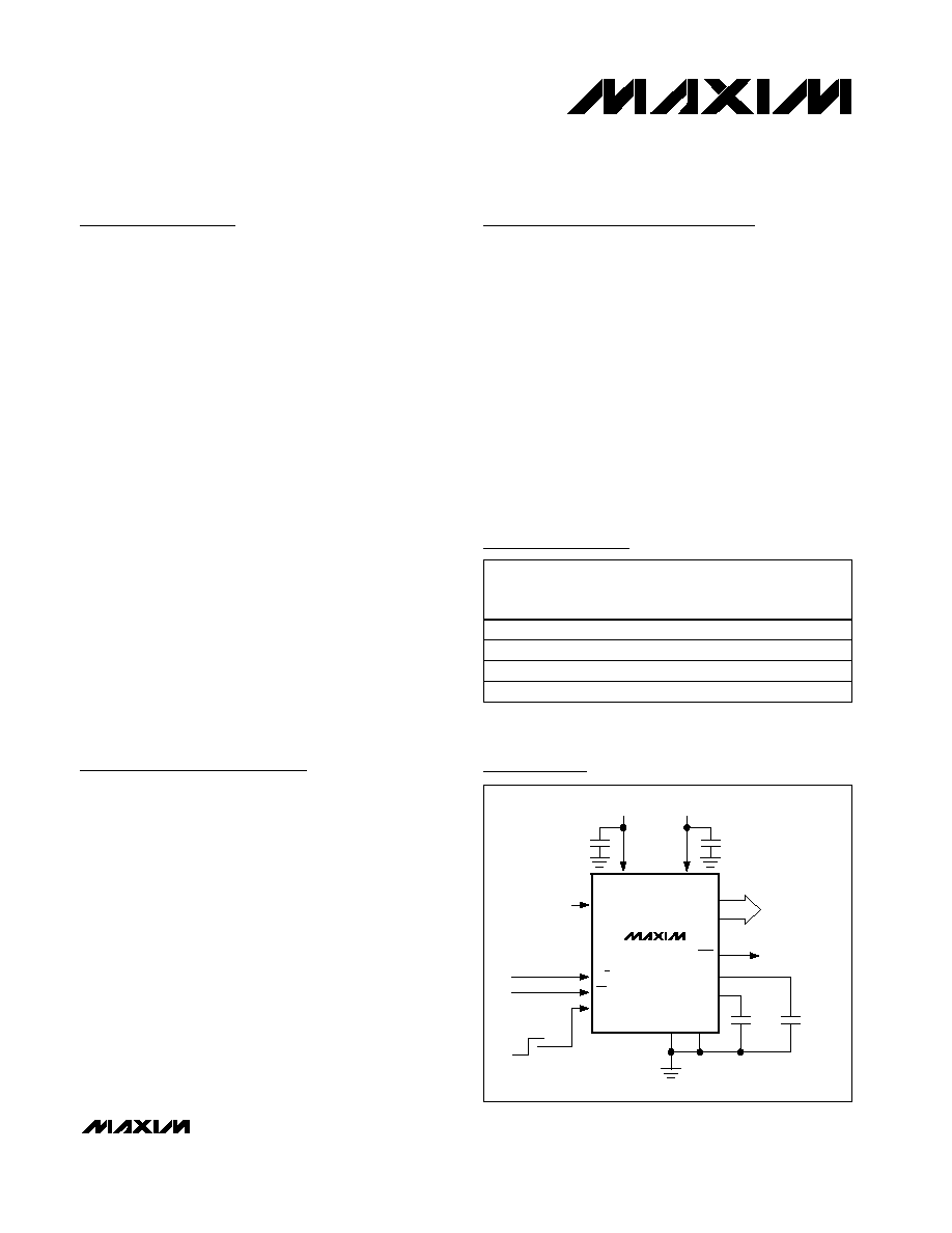
D0D7
OR
D8D13
µP DATA
BUS
AV
DD
DV
DD
AGND DGND
+5V ANALOG
+5V DIGITAL
ANALOG INPUT
AIN
HBEN
EOC
CS
R/C
REF
REFADJ
HIGH
BYTE
LOW
BYTE
10
µF
0.1
µF
0.1
µF
0.1
µF
MAX1156
MAX1158
MAX1174
Typical Operating Circuit
19-2736; Rev 0; 1/03
For pricing, delivery, and ordering information, please contact Maxim/Dallas Direct! at
1-888-629-4642, or visit Maxim's website at www.maxim-ic.com.
AutoShutdown is a trademark of Maxim Integrated Products, Inc.
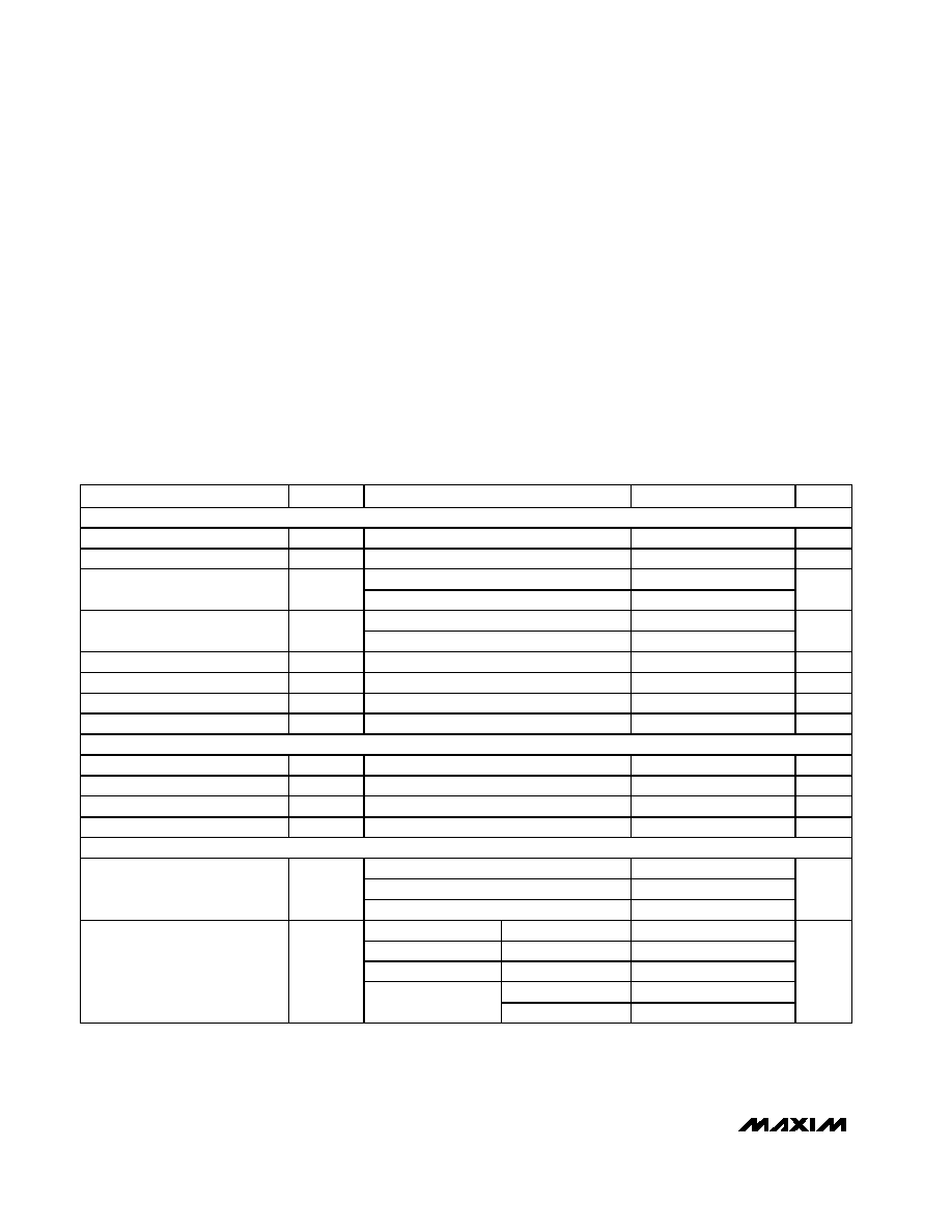
Ordering Information
PART
TEMP RANGE
PIN-
PACKAGE
INPUT
VOLTAGE
RANGE
MAX1156ACUP
0°C to +70°C
20 TSSOP
0 to +10V
MAX1156BCUP
0°C to +70°C
20 TSSOP
0 to +10V
MAX1156AEUP
-40°C to +85°C
20 TSSOP
0 to +10V
MAX1156BEUP
-40°C to +85°C
20 TSSOP
0 to +10V
Pin Configuration appears at end of data sheet.
Ordering Information continued at end of data sheet.
MAX1156/MAX1158/MAX1174
14-Bit, 135ksps, Single-Supply ADCs with
Bipolar Analog Input Range
2
_______________________________________________________________________________________
ABSOLUTE MAXIMUM RATINGS
Stresses beyond those listed under "Absolute Maximum Ratings" may cause permanent damage to the device. These are stress ratings only, and functional
operation of the device at these or any other conditions beyond those indicated in the operational sections of the specifications is not implied. Exposure to
absolute maximum rating conditions for extended periods may affect device reliability.
AV
DD
to AGND .........................................................-0.3V to +6V
DV
DD
to DGND.........................................................-0.3V to +6V
AGND to DGND.....................................................-0.3V to +0.3V
AIN to AGND .....................................................-16.5V to +16.5V
REF, REFADJ to AGND............................-0.3V to (AV
DD
+ 0.3V)
CS, R/C, HBEN to DGND .........................................-0.3V to +6V
D_, EOC to DGND ...................................-0.3V to (DV
DD
+ 0.3V)
Maximum Continuous Current into any Pin.........................50mA
Continuous Power Dissipation (T
A
= +70°C)
20-Pin TSSOP (derate 10.9mW/°C above +70°C) .......879mW
Operating Temperature Range
MAX11_ _ _CUP..................................................0°C to +70°C
MAX11_ _ _EUP ...............................................-40°C to +85°C
Storage Temperature Range .............................-65°C to +150°C
Junction Temperature ......................................................+150°C
Lead Temperature (soldering, 10s) .................................+300°C
ELECTRICAL CHARACTERISTICS
(AV
DD
= DV
DD
= +5V ±5%, external reference = +4.096V, C
REF
= 10µF, C
REFADJ
= 0.1µF, V
REFADJ
= AV
DD
, T
A
= T
MIN
to T
MAX
,
unless otherwise noted. Typical values are at T
A
= +25°C.)
PARAMETER
SYMBOL
CONDITIONS
MIN
TYP
MAX
UNITS
DC ACCURACY
Resolution
RES
14
Bits
Differential Nonlinearity
DNL
No missing codes over temperature
-1
+1
LSB
MAX11_ _A
-1
+1
Integral Nonlinearity
INL
MAX11_ _B
-2
+2
LSB
RMS noise, external reference
0.32
Transition Noise
Internal reference
0.34
LSB
RMS
Offset Error
-10
0
+10
mV
Gain Error
0
±0.2
%FSR
Offset Drift
16
µV/°C
Gain Drift
±1
ppm/°C
AC ACCURACY (f
IN
= 1kHz, V
AIN
= full range, 135ksps)
Signal-to-Noise Plus Distortion
SINAD
81
85
dB
Signal-to-Noise Ratio
SNR
82
85
dB
Total Harmonic Distortion
THD
-100
-86
dB
Spurious-Free Dynamic Range
SFDR
87
103
dB
ANALOG INPUT
MAX1156
0
+10
MAX1158
-10
+10
Input Range
V
AIN
MAX1174
-5
+5
V
MAX1156/MAX1174
Normal operation
5.3
6.9
9.2
MAX1156
Shutdown mode
5.3
MAX1174
Shutdown mode
3.0
Normal operation
7.8
10
13.0
Input Resistance
R
AIN
MAX1158
Shutdown mode
6.0
k
MAX1156/MAX1158/MAX1174
14-Bit, 135ksps, Single-Supply ADCs with
Bipolar Analog Input Range
_______________________________________________________________________________________
3
ELECTRICAL CHARACTERISTICS (continued)
(AV
DD
= DV
DD
= +5V ±5%, external reference = +4.096V, C
REF
= 10µF, C
REFADJ
= 0.1µF, V
REFADJ
= AV
DD
, T
A
= T
MIN
to T
MAX
,
unless otherwise noted. Typical values are at T
A
= +25°C.)
PARAMETER
SYMBOL
CONDITIONS
MIN
TYP
MAX
UNITS
MAX1156, 0
V
AIN
+10V
-0.1
+2.0
Normal operation
-1.8
+1.2
MAX1158,
-10V
V
AIN
+10V
Shutdown mode
-1.8
+1.8
Normal operation
-1.8
+0.4
Input Current
I
AIN
MAX1174,
-5V
V
AIN
+5V
Shutdown mode
-1.8
+1.8
mA
MAX1158, V
AIN
= +10V, shutdown mode to
operating mode
0.5
0.7
Input Current Step at Power-Up
I
PU
MAX1174, V
AIN
= +5V, shutdown mode to
operating mode
1
1.4
mA
Input Capacitance
C
IN
10
pF
INTERNAL REFERENCE
REF Output Voltage
V
REF
4.056
4.096
4.136
V
REF Output Tempco
±35
ppm/°C
REF Short-Circuit Current
I
REF-SC
±10
mA
EXTERNAL REFERENCE
REF and REFADJ Input Voltage
Range
3.8
4.2
V
REFADJ Buffer Disable Threshold
AV
DD
-
0.4
AV
DD
-
0.1
V
Normal mode, f
SAMPLE
= 135ksps
60
100
REF Input Current
I
REF
Shutdown mode (Note 1)
±0.1
±10
µA
REFADJ Input Current
I
REFADJ
REFADJ = AV
DD
16
µA
DIGITAL INPUTS/OUTPUTS
Output High Voltage
V
OH
I
SOURCE
= 0.5mA, DV
DD
= +2.7V to +5.25V,
AV
DD
= +5.25V
DV
DD
-
0.4
V
Output Low Voltage
V
OL
I
SINK
= 1.6mA, DV
DD
= +2.7V to +5.25V,
AV
DD
= +5.25V
0.4
V
Input High Voltage
V
IH
0.7
×
DV
DD
V
Input Low Voltage
V
IL
0.3
×
DV
DD
V
Input Leakage Current
Digital input = DV
DD
or 0V
-1
+1
µA
Input Hysteresis
V
HYST
0.2
V
Input Capacitance
C
IN
15
pF
Three-State Output Leakage
I
OZ
±10
µA
Three-State Output Capacitance
C
OZ
15
pF
MAX1156/MAX1158/MAX1174
14-Bit, 135ksps, Single-Supply ADCs with
Bipolar Analog Input Range
4
_______________________________________________________________________________________
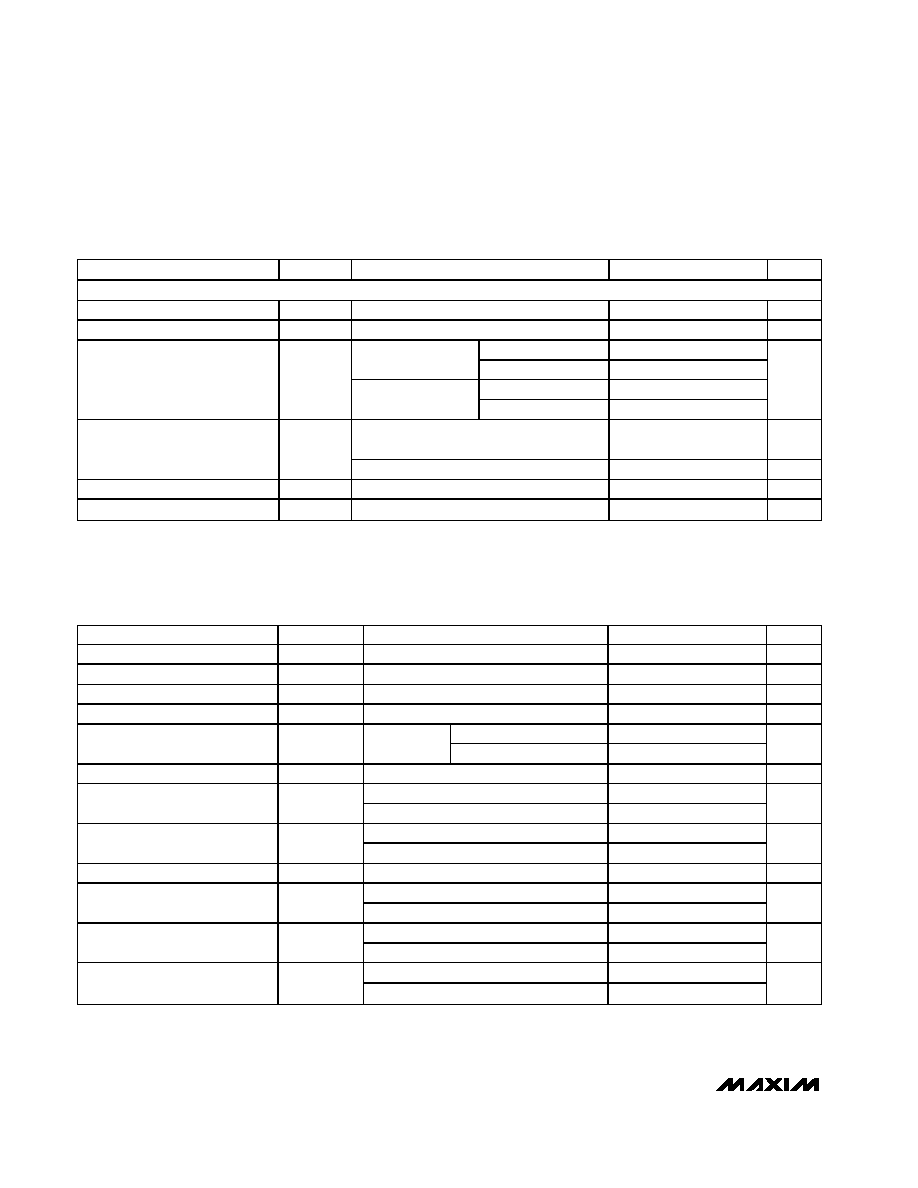
TIMING CHARACTERISTICS (Figures 1 and 2)
(AV
DD
= +4.75V to +5.25V ±5%, DV
DD
= +2.7V to AV
DD
, external reference = +4.096V, C
REF
= 10µF, C
REFADJ
= 0.1µF, V
REFADJ
=
AV
DD
, C
LOAD
= 20pF, T
A
= T
MIN
to T
MAX
.)
PARAMETER
SYMBOL
CONDITIONS
MIN
TYP
MAX
UNITS
Maximum Sampling Rate
f
SAMPLE-MAX
135
ksps
Acquisition Time
t
ACQ
2
µs
Conversion Time
t
CONV
4.7
µs
CS Pulse Width High
t
CSH
(Note 2)
40
ns
DV
DD
= +4.75V to +5.25V
40
CS Pulse Width Low
t
CSL
(Note 2)
DV
DD
= +2.7V to +5.25V
60
ns
R/C to CS Fall Setup Time
t
DS
0
ns
DV
DD
= +4.75V to +5.25V
40
R/C to CS Fall Hold Time
t
DH
DV
DD
= +2.7V to +5.25V
60
ns
DV
DD
= +4.75V to +5.25V
40
CS to Output Data Valid
t
DO
DV
DD
= +2.7V to +5.25V
80
ns
EOC Fall to CS Fall
t
DV
0
ns
DV
DD
= +4.75V to +5.25V
40
CS Rise to EOC Rise
t
EOC
DV
DD
= +2.7V to +5.25V
80
ns
DV
DD
= +4.75V to +5.25V
40
Bus Relinquish Time
t
BR
DV
DD
= +2.7V to +5.25V
80
ns
DV
DD
= +4.75V to +5.25V
40
HBEN Transition to Output Data
Valid
t
DO
1
DV
DD
= +2.7V to +5.25V
80
ns
ELECTRICAL CHARACTERISTICS (continued)
(AV
DD
= DV
DD
= +5V ±5%, external reference = +4.096V, C
REF
= 10µF, C
REFADJ
= 0.1µF, V
REFADJ
= AV
DD
, T
A
= T
MIN
to T
MAX
,
unless otherwise noted. Typical values are at T
A
= +25°C.)
PARAMETER
SYMBOL
CONDITIONS
MIN
TYP
MAX
UNITS
POWER SUPPLIES
Analog Supply Voltage
AV
DD
4.75
5.25
V
Digital Supply Voltage
DV
DD
2.70
5.25
V
MAX1156
2.9
External reference,
135ksps
MAX1158/MAX1174
4
5.3
MAX1156
3.8
Analog Supply Current
I
AVDD
Internal reference,
135ksps
MAX1158/MAX1174
5.2
6.2
mA
Shutdown mode (Note 1), digital input =
DV
DD
or 0V
0.5
5
µA
Shutdown Supply Current
I
SHDN
Standby mode
3.7
mA
Digital Supply Current
I
DVDD
0.75
mA
Power-Supply Rejection
AV
DD
= DV
DD
= +4.75V to +5.25V
1
LSB
Note 1: Maximum specification is limited by automated test equipment.
Note 2: To ensure best performance, finish reading the data and wait t
BR
before starting a new acquisition.
MAX1156/MAX1158/MAX1174
14-Bit, 135ksps, Single-Supply ADCs with
Bipolar Analog Input Range
_______________________________________________________________________________________
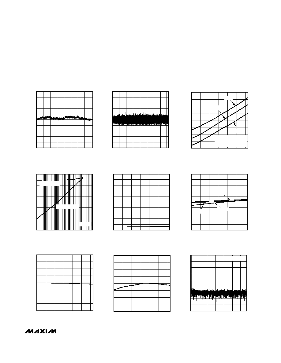
5
INL vs. CODE
MAX1156/58/74 toc01
-2.5
-1.5
-2.0
-0.5
-1.0
0.5
0
1.0
2.0
1.5
2.5
INL (LSB)
0
4000 6000 8000
2000
10000 12000 14000 16000
CODE
DNL vs. CODE
MAX1156/58/74 toc02
-1.0
-0.6
-0.8
-0.2
-0.4
0.2
0
0.4
0.8
0.6
1.0
DNL (LSB)
0
4000 6000 8000
2000
10000 12000 14000 16000
CODE
4.40
4.50
4.45
4.60
4.55
4.75
4.70
4.65
4.80
-40
0
-20
20
40
60
80
SUPPLY CURRENT (AV
DD
+ DV
DD
)
vs. TEMPERATURE
MAX1156/58/74 toc03
TEMPERATURE (
°C)
SUPPLY CURRENT (mA)
5.25V
5.0V
4.75V
f
SAMPLE
= 135ksps
SHUTDOWN MODE
BETWEEN CONVERSIONS
SUPPLY CURRENT (AV
DD
+ DV
DD
)
vs. SAMPLE RATE
MAX1156/58/74 toc04
SAMPLE RATE (ksps)
SUPPLY CURRENT (mA)
100
10
1
0.1
0.001
0.01
0.1
1
10
0.0001
0.01
1000
V
AIN
= 0V
SHUTDOWN MODE
STANDBY MODE
0
1.5
1.0
0.5
2.5
2.0
4.5
4.0
3.5
3.0
5.0
-40
-20
0
20
40
60
80
SHUTDOWN CURRENT (AV
DD
+ DV
DD
)
vs. TEMPERATURE
MAX1156/58/74 toc05
TEMPERATURE (
°C)
SHUTDOWN SUPPLY CURRENT (
µ
A)
NO CONVERSIONS
-10
-4
-6
-8
0
-2
8
6
4
2
10
-40
-20
0
20
40
60
80
OFFSET ERROR vs. TEMPERATURE
MAX1156/58/74 toc06
TEMPERATURE (
°C)
OFFSET ERROR (mV)
MAX1174
MAX1158
MAX1156
-0.20
-0.10
-0.15
0
-0.05
0.15
0.10
0.05
0.20
-40
0
-20
20
40
60
80
GAIN ERROR vs. TEMPERATURE
MAX1156/58/74 toc07
TEMPERATURE (
°C)
GAIN ERROR (%FSR)
4.056
4.076
4.066
4.096
4.086
4.126
4.116
4.106
4.136
-40
0
-20
20
40
60
80
INTERNAL REFERENCE
vs. TEMPERATURE
MAX1156/58/74 toc08
TEMPERATURE (
°C)
INTERNAL REFERENCE (V)
-180
-140
-160
-80
-100
-120
-20
-40
-60
0
0
20
30
10
40
50
60
FFT AT 1kHz
MAX1156/58/74 toc09
FREQUENCY (kHz)
MAGNITUDE (dB)
f
SAMPLE
= 131ksps
Typical Operating Characteristics
(AV
DD
= DV
DD
= +5V, external reference = +4.096V, C
REF
= 10µF, C
REFADJ
= 0.1µF, V
REFADJ
= AV
DD
, C
LOAD
= 20pF, T
A
= T
MIN
to
T
MAX
, unless otherwise noted. Typical values are at T
A
= +25°C.) (Typical Application Circuit)