Äîêóìåíòàöèÿ è îïèñàíèÿ www.docs.chipfind.ru
General Description
The MAX1192 is an ultra-low-power, dual, 8-bit, 22Msps
analog-to-digital converter (ADC). The device features
two fully differential wideband track-and-hold (T/H) inputs.
These inputs have a 440MHz bandwidth and accept fully
differential or single-ended signals. The MAX1192 deliv-
ers a typical signal-to-noise and distortion (SINAD) of
48.6dB at an input frequency of 5.5MHz and a sampling
rate of 22Msps while consuming only 27.3mW. This ADC
operates from a 2.7V to 3.6V analog power supply. A sep-
arate 1.8V to 3.6V supply powers the digital output driver.
In addition to ultra-low operating power, the MAX1192
features three power-down modes to conserve power
during idle periods. Excellent dynamic performance,
ultra-low power, and small size make the MAX1192 ideal
for applications in imaging, instrumentation, and digital
communications.
An internal 1.024V precision bandgap reference sets
the full-scale range of the ADC to ±0.512V. A flexible
reference structure allows the MAX1192 to use its inter-
nal reference or accept an externally applied reference
for applications requiring increased accuracy.
The MAX1192 features parallel, multiplexed, CMOS-
compatible tri-state outputs. The digital output format is
offset binary. A separate digital power input accepts a
voltage from 1.8V to 3.6V for flexible interfacing to dif-
ferent logic levels. The MAX1192 is available in a 5mm
× 5mm, 28-pin thin QFN package, and is specified for
the extended industrial (-40°C to +85°C) temperature
range.
For higher sampling frequency applications, refer to the
MAX1195MAX1198 dual 8-bit ADCs. Pin-compatible
versions of the MAX1192 are also available. Refer to the
MAX1191 data sheet for 7.5Msps, and the MAX1193
data sheet for 45Msps.
Applications
Ultrasound and Medical Imaging
IQ Baseband Sampling
Battery-Powered Portable Instruments
Low-Power Video
WLAN, Mobile DSL, WLL Receiver
Features
o Ultra-Low Power
27.3mW (Normal Operation: 22Msps)
1.8µW (Shutdown Mode)
o Excellent Dynamic Performance
48.6dB/47.2dB SNR at f
IN
= 5.5MHz/125MHz
70dBc/69dBc SFDR at f
IN
= 5.5MHz/125MHz
o 2.7V to 3.6V Single Analog Supply
o 1.8V to 3.6V TTL/CMOS-Compatible Digital
Outputs
o Fully Differential or Single-Ended Analog Inputs
o Internal/External Reference Option
o Multiplexed CMOS-Compatible Tri-State Outputs
o 28-Pin Thin QFN Package
o Evaluation Kit Available (Order MAX1193EVKIT)
MAX1192
Ultra-Low-Power, 22Msps, Dual 8-Bit ADC
________________________________________________________________ Maxim Integrated Products
1
28
27
26
25
24
23
22
8
9
10
11
12
13
14
15
16
17
18
19
20
21
7
6
5
4
3
2
1
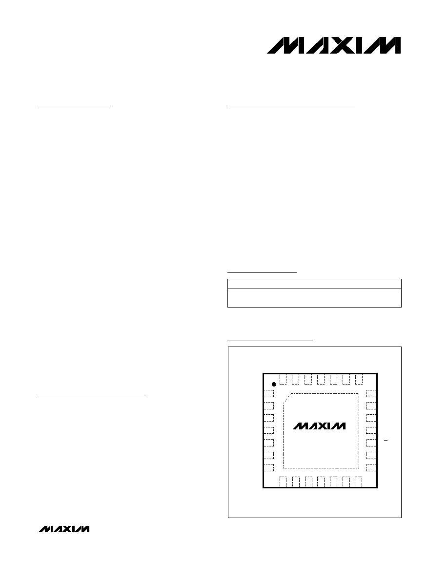
MAX1192
5mm x 5mm THIN QFN
TOP VIEW
INA+
EXPOSED PADDLE
INA-
GND
CLK
GND
INB+
INB-
V
DD
REFP
REFN
COM
REFIN
PD0
PD1
D0
D1
D2
D3
A/B
D4
D5
D6
D7
OV
DD
OGND
GND
V
DD
V
DD
Pin Configuration
Ordering Information
19-2835; Rev 1; 9/03
For pricing, delivery, and ordering information, please contact Maxim/Dallas Direct! at
1-888-629-4642, or visit Maxim's website at www.maxim-ic.com.
PART
TEMP RANGE
PIN-PACKAGE
MAX1192ETI-T
-40°C to +85°C
28 Thin QFN-EP*
(5mm x 5mm)
*EP = Exposed paddle.
MAX1192
Ultra-Low-Power, 22Msps, Dual 8-Bit ADC
2
_______________________________________________________________________________________
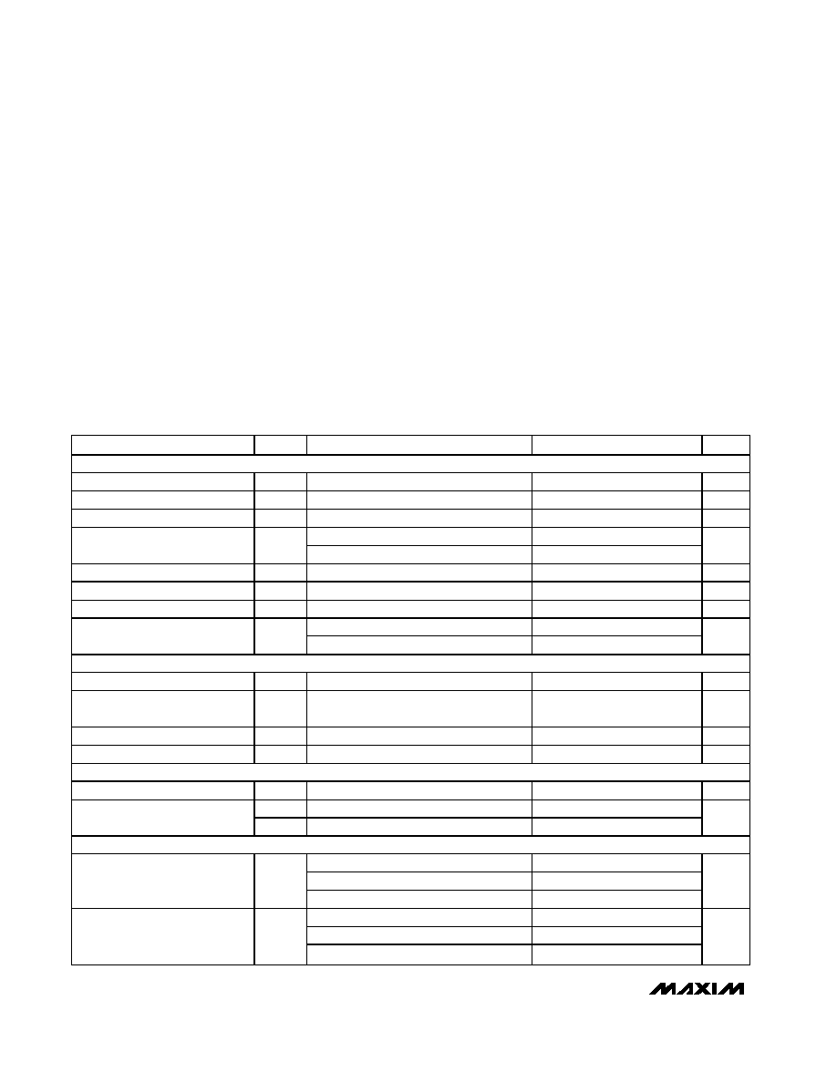
ABSOLUTE MAXIMUM RATINGS
ELECTRICAL CHARACTERISTICS
(V
DD
= 3.0V, OV
DD
= 1.8V, V
REFIN
= V
DD
(internal reference), C
L
10pF at digital outputs, f
CLK
= 22MHz, C
REFP
= C
REFN
= C
COM
=
0.33µF, T
A
= -40°C to +85°C, unless otherwise noted. Typical values are at T
A
= +25°C.) (Note 1)
Stresses beyond those listed under "Absolute Maximum Ratings" may cause permanent damage to the device. These are stress ratings only, and functional
operation of the device at these or any other conditions beyond those indicated in the operational sections of the specifications is not implied. Exposure to
absolute maximum rating conditions for extended periods may affect device reliability.
V
DD
, OV
DD
to GND ...............................................-0.3V to +3.6V
OGND to GND.......................................................-0.3V to +0.3V
INA+, INA-, INB+, INB- to GND .................-0.3V to (V
DD
+ 0.3V)
CLK, REFIN, REFP, REFN, COM to GND ...-0.3V to (V
DD
+ 0.3V)
PD0, PD1 to OGND .................................-0.3V to (OV
DD
+ 0.3V)
Digital Outputs to OGND .........................-0.3V to (OV
DD
+ 0.3V)
Continuous Power Dissipation (T
A
= +70°C)
28-Pin Thin QFN (derated 20.8mW/°C above +70°C) ..1667mW
Operating Temperature Range ...........................-40°C to +85°C
Junction Temperature ......................................................+150°C
Storage Temperature Range ............................-65°C to +150°C
Lead Temperature (soldering, 10s) .................................+300°C
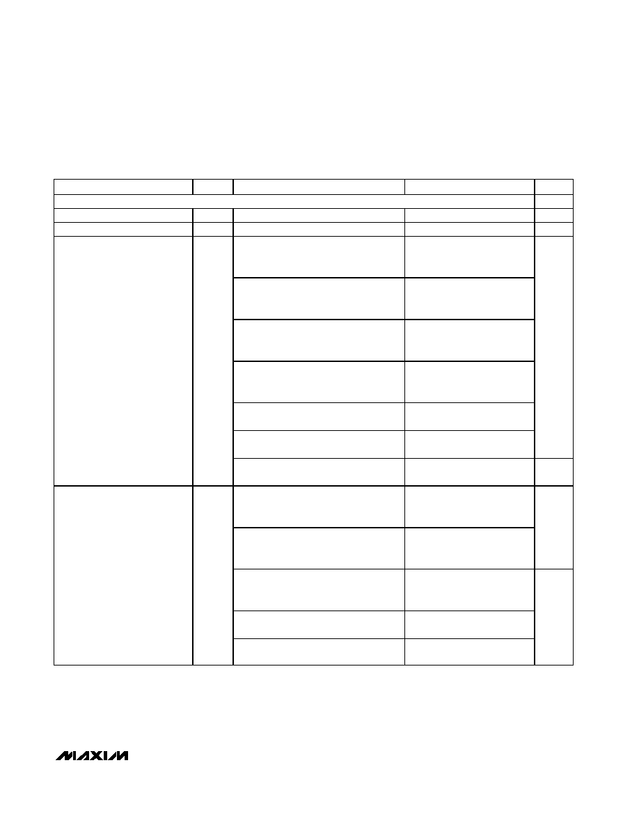
PARAMETER
SYMBOL
CONDITIONS
MIN
TYP
MAX
UNITS
DC ACCURACY
Resolution
8
Bits
Integral Nonlinearity
INL
±0.15
±1.00
LSB
Differential Nonlinearity
DNL
No missing codes over temperature
±0.14
±1.00
LSB
+25°C
±4
Offset Error
< +25°C
±6
%FS
Gain Error
Excludes REFP - REFN error
±2
%FS
DC Gain Matching
±0.01
±0.2
dB
Gain Temperature Coefficient
±30
ppm/°C
Offset (V
DD
±5%)
±0.02
Power-Supply Rejection
Gain (V
DD
±5%)
±0.05
LSB
ANALOG INPUT
Differential Input Voltage Range
V
DIFF
Differential or single-ended inputs
±0.512
V
Common-Mode Input Voltage
Range
V
COM
V
DD
/
2
V
Input Resistance
R
IN
Switched capacitor load
245
k
Input Capacitance
C
IN
5
pF
CONVERSION RATE
Clock Frequency Range
f
CLK
7.5
22
MHz
Channel A
5.0
Data Latency
Channel B
5.5
Clock
cycles
DYNAMIC CHARACTERISTICS (differential inputs, 4096-point FFT)
f
IN
= 1.875MHz
48.6
f
IN
= 5.5MHz
47
48.6
Signal-to-Noise Ratio
(Note 2)
SNR
f
IN
= 11MHz
48.6
dB
f
IN
= 1.875MHz
48.7
f
IN
= 5.5MHz
47
48.6
Signal-to-Noise and Distortion
(Note 2)
SINAD
f
IN
= 11MHz
48.6
dB
MAX1192
Ultra-Low-Power, 22Msps, Dual 8-Bit ADC
_______________________________________________________________________________________
3
ELECTRICAL CHARACTERISTICS (continued)
(V
DD
= 3.0V, OV
DD
= 1.8V, V
REFIN
= V
DD
(internal reference), C
L
10pF at digital outputs, f
CLK
= 22MHz, C
REFP
= C
REFN
= C
COM
=
0.33µF, T
A
= -40°C to +85°C, unless otherwise noted. Typical values are at T
A
= +25°C.) (Note 1)
PARAMETER
SYMBOL
CONDITIONS
MIN
TYP
MAX
UNITS
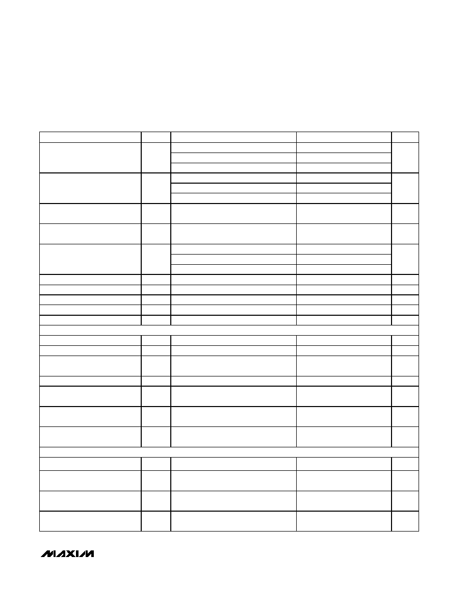
f
IN
= 1.875MHz
70.8
f
IN
= 5.5MHz
59.0
70.0
Spurious-Free Dynamic Range
(Note 2)
SFDR
f
IN
= 11MHz
70.4
dBc
f
IN
= 1.875MHz
75.8
f
IN
= 5.5MHz
-74.0
Thi r d - H ar m oni c D i stor ti on
( N ote 2)
HD3
f
IN
= 11MHz
-74.8
dBc
Intermodulation Distortion
IMD
f
IN1
= 1MHz at -7dB FS, f
IN2
= 1.01MHz at
-7dB FS
-64
dBc
Third-Order Intermodulation
IM3
f
IN1
= 1MHz at -7dB FS, f
IN2
= 1.01MHz at
-7dB FS
-67
dBc
f
IN
= 1.875MHz
-71.0
f
IN
= 5.5MHz
-70.0
-57.0
Total Harmonic Distortion
(Note 2)
THD
f
IN
= 11MHz
-70.2
dBc
Small-Signal Bandwidth
SSBW
Input at -20dB FS
440
MHz
Full-Power Bandwidth
FPBW
Input at -0.5dB FS
440
MHz
Aperture Delay
t
AD
1.5
ns
Aperture Jitter
t
AJ
2
ps
RMS
Overdrive Recovery Time
1.5
× full-scale input
2
ns
INTERNAL REFERENCE (REFIN = V
DD
; V
REFP
, V
REFN
, and V
COM
are generated internally)
REFP Output Voltage
V
REFP
- V
COM
0.256
V
REFN Output Voltage
V
REFN
- V
COM
-0.256
V
COM Output Voltage
V
COM
V
DD
/ 2
- 0.15
V
DD
/ 2
V
DD
/ 2
+ 0.15
V
Differential Reference Output
V
REF
V
REFP
- V
REFN
0.512
V
Differential Reference Output
Temperature Coefficient
V
REFTC
±30
ppm/°C
Maximum REFP/REFN/COM
Source Current
I
SOURCE
2
mA
Maximum REFP/REFN/COM Sink
Current
I
SINK
2
mA
BUFFERED EXTERNAL REFERENCE (V
REFIN
= 1.024V, V
REFP
, V
REFN
, and V
COM
are generated internally)
REFIN Input Voltage
V
REFIN
1.024
V
COM Output Voltage
V
COM
V
DD
/ 2
- 0.15
V
DD
/ 2
V
DD
/ 2
+ 0.15
V
Differential Reference Output
V
REF
V
REFP
- V
REFN
0.512
V
Maximum REFP/REFN/COM
Source Current
I
SOURCE
2
mA
PARAMETER
SYMBOL
CONDITIONS
MIN
TYP
MAX
UNITS
Maximum REFP/REFN/COM Sink
Current
I
SINK
2
mA
REFIN Input Resistance
>500
k
REFIN Input Current
-0.7
µA
UNBUFFERED EXTERNAL REFERENCE (REFIN = GND, V
REFP
, V
REFN
, and V
COM
are applied externally)
REFP Input Voltage
V
REFP
- V
COM
0.256
V
REFN Input Voltage
V
REFN
- V
COM
-0.256
V
COM Input Voltage
V
COM
V
DD
/ 2
V
Differential Reference Input
Voltage
V
REF
V
REFP
- V
REFN
0.512
V
REFP Input Resistance
R
REFP
Measured between REFP and COM
4
k
REFN Input Resistance
R
REFN
Measured between REFN and COM
4
k
DIGITAL INPUTS (CLK, PD0, PD1)
CLK
0.7 x
V
DD
Input High Threshold
V
IH
PD0, PD1
0.7 x
OV
DD
V
CLK
0.3 x
V
DD
Input Low Threshold
V
IL
PD0, PD1
0.3 x
OV
DD
V
Input Hysteresis
V
HYST
0.1
V
CLK at GND or V
DD
±5
Digital Input Leakage Current
DI
IN
PD0 and PD1 at OGND or OV
DD
±5
µA
Digital Input Capacitance
DC
IN
5
pF
DIGITAL OUTPUTS (D7D0, A/
B)
Output Voltage Low
V
OL
I
SINK
= 200µA
0.2 x
OV
DD
V
Output Voltage High
V
OH
I
SOURCE
= 200µA
0.8 x
OV
DD
V
Tri-State Leakage Current
I
LEAK
±5
µA
Tri-State Output Capacitance
C
OUT
5
pF
MAX1192
Ultra-Low-Power, 22Msps, Dual 8-Bit ADC
4
_______________________________________________________________________________________
ELECTRICAL CHARACTERISTICS (continued)
(V
DD
= 3.0V, OV
DD
= 1.8V, V
REFIN
= V
DD
(internal reference), C
L
10pF at digital outputs, f
CLK
= 22MHz, C
REFP
= C
REFN
= C
COM
=
0.33µF, T
A
= -40°C to +85°C, unless otherwise noted. Typical values are at T
A
= +25°C.) (Note 1)
MAX1192
Ultra-Low-Power, 22Msps, Dual 8-Bit ADC
_______________________________________________________________________________________
5
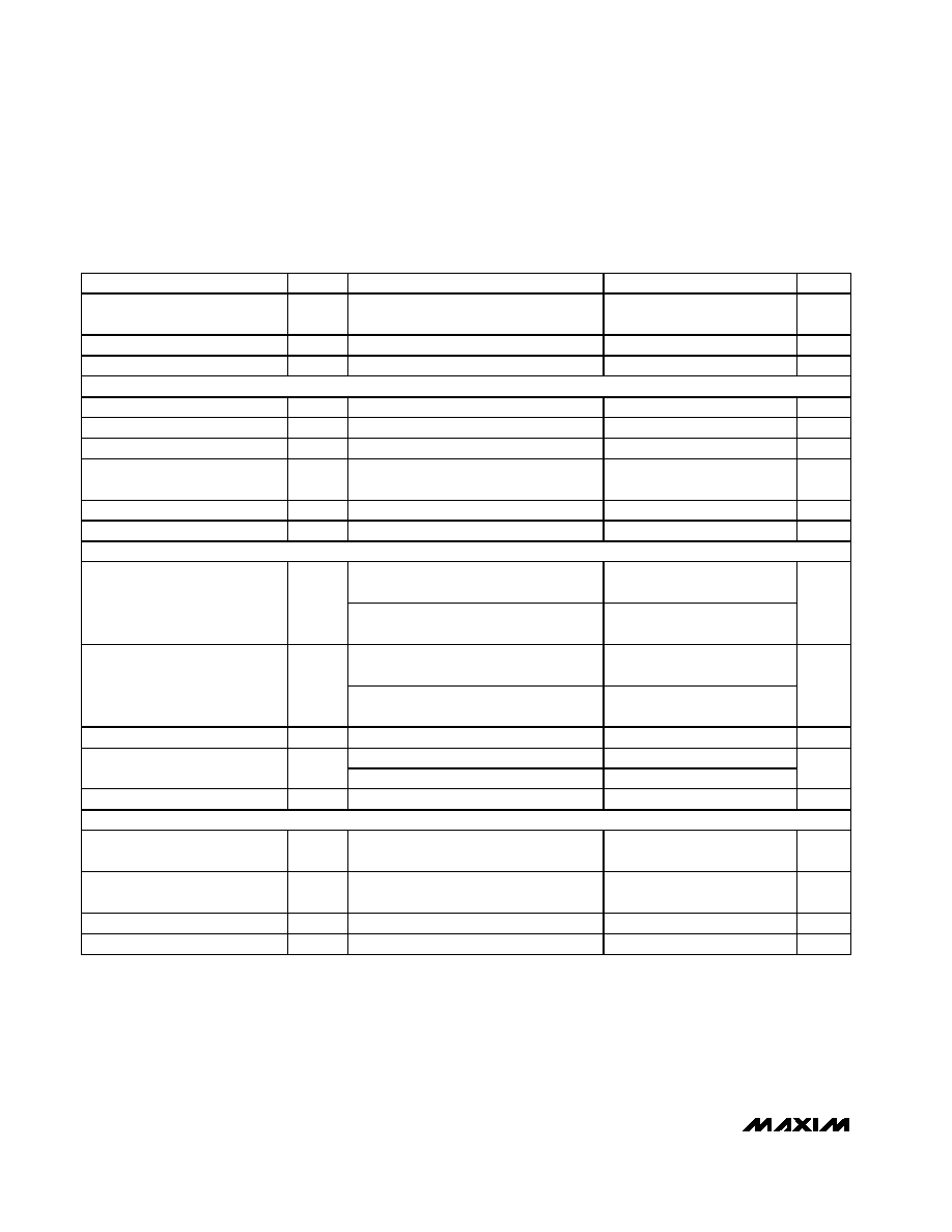
PARAMETER
SYMBOL
CONDITIONS
MIN
TYP
MAX
UNITS
POWER REQUIREMENTS
Analog Supply Voltage
V
DD
2.7
3.0
3.6
V
Digital Output Supply Voltage
OV
DD
1.8
V
DD
V
Normal operating mode, f
IN
= 1.875MHz
at -0.5dB FS, f
CLK
= 7.5MHz,
CLK input from GND to V
DD
4.2
5.0
Normal operating mode, f
IN
= 5.5MHz
at -0.5dB FS, f
CLK
= 22MHz,
CLK input from GND to V
DD
9.1
10.5
Idle mode (tri-state), f
IN
= 1.875MHz at -
0.5dB FS, f
CLK
= 7.5MHz, CLK input from
GND to V
DD
4.2
Idle mode (tri-state), f
IN
= 5.5MHz at
-0.5dB FS, f
CLK
= 22MHz, CLK input from
GND to V
DD
9.1
Standby mode, f
CLK
= 7.5MHz, CLK input
from GND to V
DD
2.3
Standby mode, f
CLK
= 22MHz, CLK input
from GND to V
DD
4.9
mA
Analog Supply Current
I
DD
Shutdown mode, CLK = GND or V
DD
,
PD0 = PD1 = OGND
0.6
5.0
µA
Normal operating mode,
f
IN
= 1.875MHz at -0.5dB FS,
f
CLK
= 7.5MHz, C
L
10pF
1.0
Normal operating mode,
f
IN
= 5.5MHz at -0.5dB FS,
f
CLK
= 22MHz, C
L
10pF
2.9
mA
Idle mode (tri-state), DC input,
CLK = GND or V
DD,
PD0 = OV
DD
, PD1 = OGND
0.1
5.0
Standby mode, DC input, CLK = GND or
V
DD,
PD0 = OGND, PD1 = OV
DD
0.1
Digital Output Supply Current
(Note 3)
I
ODD
Shutdown mode, CLK = GND or V
DD
,
PD0 = PD1 = OGND
0.1
5.0
µA
ELECTRICAL CHARACTERISTICS (continued)
(V
DD
= 3.0V, OV
DD
= 1.8V, V
REFIN
= V
DD
(internal reference), C
L
10pF at digital outputs, f
CLK
= 22MHz, C
REFP
= C
REFN
= C
COM
=
0.33µF, T
A
= -40°C to +85°C, unless otherwise noted. Typical values are at T
A
= +25°C.) (Note 1)