
For free samples & the latest literature: http://www.maxim-ic.com, or phone 1-800-998-8800.
For small orders, phone 1-800-835-8769.
General Description
The MAX1205 is a 14-bit, monolithic, analog-to-digital
converter (ADC) capable of conversion rates up to
1Msps. This integrated circuit, built on a CMOS pro-
cess, uses a fully differential, pipelined architecture
with digital error correction and a short self-calibration
procedure that corrects for capacitor and gain mis-
matches and ensures 14-bit linearity at full sample
rates. An on-chip track/hold (T/H) maintains superb
dynamic performance up to the Nyquist frequency. The
MAX1205 operates from a single +5V supply.
The fully differential inputs allow an input swing of
±V
REF
. The reference is also differential, with the posi-
tive reference (RFPF) typically connected to +4.096V
and the negative reference (RFNF) connected to ana-
log ground. Additional sensing pins (RFPS, RFNS) are
provided to compensate for any resistive-divider action
that may occur due to finite internal and external resis-
tances in the reference traces and the on-chip resis-
tance of the reference pins. A single-ended input is
also possible using two operational amplifiers.
The power dissipation is typically 257mW at +5V, at a
sampling rate of 1Msps. The device employs a CMOS-
compatible, 14-bit parallel, two's complement output
data format. For higher sampling rates, the MAX1201 is
a 2.2Msps pin-compatible upgrade to the MAX1205.
The MAX1205 is available in an MQFP package, and
operates over the commercial (0∞C to +70∞C) and the
extended (-40∞C to +85∞C) temperature ranges.
Applications
Imaging
Communications
Medical
Scanners
Data Acquisition
Features
o
Monolithic, 14-Bit, 1Msps ADC
o
+5V Single Supply
o
SNR of 80dB for f
IN
= 500kHz
o
SFDR of 87dB for f
IN
= 500kHz
o
Low Power Dissipation: 257mW
o
On-Demand Self-Calibration
o
Differential Nonlinearity Error: ±0.3LSB
o
Integral Nonlinearity Error: ±1.2LSB
o
Three-State, Two's Complement Output Data
MAX1205
+5V Single-Supply, 1Msps, 14-Bit
Self-Calibrating ADC
________________________________________________________________
Maxim Integrated Products
1
OE
DAV
CLK
DV
DD
DGND
DGND
DV
DD
TEST1
TEST2
TEST3
D0
ST_CAL
AGND
AV
DD
AGND
AGND
AV
DD
DOR
D13
D12
D11
D10
1
2
3
4
5
6
7
8
9
10
11
12
13
14
15
16
17
18
19
20
21
22
44
43
42
41
40
39
38
37
36
35
34
33
32
31
30
29
28
27
26
25
24
23
D9
D8
D7
D6
DRV
DD
DGND
D5
D4
D3
D2
D1
END_CAL
INN
N.C.
N.C.
INP
RFNS
RFNF
RFPS
RFPF
CM
TEST0
TOP VIEW
MQFP
MAX1205
19-4794; Rev 0; 11/98
PART
MAX1205CMH
MAX1205EMH
-40∞C to +85∞C
0∞C to +70∞C
TEMP. RANGE
PIN-PACKAGE
44 MQFP
44 MQFP
EVALUATION KIT
AVAILABLE
Pin Configuration
Ordering Information
MAX1205
+5V Single-Supply, 1Msps, 14-Bit
Self-Calibrating ADC
2
_______________________________________________________________________________________
ABSOLUTE MAXIMUM RATINGS
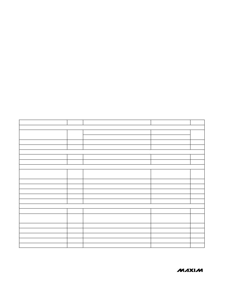
ELECTRICAL CHARACTERISTICS
(AV
DD
= +5V ±5%, DV
DD
= DRV
DD
= +3.3V, V
RFPS
= +4.096V, V
RFNS
= AGND, V
CM
= +2.048V, V
IN
= -0.5dBFS, f
CLK
= 2.048MHz,
digital output load
20pF, T
A
= T
MIN
to T
MAX
, unless otherwise noted. Typical values are at T
A
= +25∞C.) (Note 1)
Stresses beyond those listed under "Absolute Maximum Ratings" may cause permanent damage to the device. These are stress ratings only, and functional
operation of the device at these or any other conditions beyond those indicated in the operational sections of the specifications is not implied. Exposure to
absolute maximum rating conditions for extended periods may affect device reliability.
AV
DD
to AGND, DGND ..........................................................+7V
DV
DD
to DGND, AGND..........................................................+7V
DRV
DD
to DGND, AGND .......................................................+7V
INP, INN, RFPF, RFPS, RFNF, RFNS,
CLK, CM.................................(AGND - 0.3V) to (AV
DD
+ 0.3V)
Digital Inputs to DGND ............................-0.3V to (DV
DD
+ 0.3V)
Digital Output (DAV) to DGND ..............-0.3V to (DRV
DD
+ 0.3V)
Other Digital Outputs to DGND .............-0.3V to (DRV
DD
+ 0.3V)
Continuous Power Dissipation (T
A
= +70∞C)
44-Pin MQFP (derate 11.11mW/∞C above +70∞C)........889mW
Operating Temperature Ranges (T
A
)
MAX1205CMH .....................................................0∞C to +70∞C
MAX1205EMH ..................................................-40∞C to +85∞C
Storage Temperature Range .............................-65∞C to +150∞C
Lead Temperature (soldering, 10sec) .............................+300∞C
REFERENCE/EXTERNAL
TRANSFER CHARACTERISTICS
DYNAMIC SPECIFICATIONS
(Note 6)
ANALOG INPUT
To full-scale step (0.006%)
ns
3
t
AD
Aperture Delay
ns
410
t
OVR
ns
100
t
ACQ
Acquisition Time
Overvoltage Recovery Time
MHz
3.3
Full-Power Bandwidth
MHz
78
Small-Signal Bandwidth
After calibration, guaranteed
f
SAMPLE =
f
CLK /
2
LSB
-1
±0.3
+1
DNL
Differential Nonlinearity
LSB
±1.2
INL
Bits
14
RES
Resolution (no missing codes)
(Note 5)
Integral Nonlinearity
f
SAMPLE
Cycles
4
Conversion Time (Pipeline
Delay/Latency)
Msps
1.024
f
SAMPLE
Maximum Sampling Rate
%FSR
-0.2
±0.003
+0.2
Offset Error
%FSR
-5
-3.0
+5
Gain Error
µV
RMS
75
Input-Referred Noise
Differential
Single-ended
Per side in track mode
CONDITIONS
±4.096
±4.5
V
4.096
4.5
V
IN
Input Voltage Range
(Notes 2, 3)
700
1000
Reference Input Resistance
k
55
R
I
Input Resistance (Note 4)
pF
21
C
I
Input Capacitance (Note 3)
V
4.096
4.5
V
REF
Reference Voltage (Note 3)
UNITS
MIN
TYP
MAX
SYMBOL
PARAMETER

MAX1205
+5V Single-Supply, 1Msps, 14-Bit
Self-Calibrating ADC
_______________________________________________________________________________________
3
ELECTRICAL CHARACTERISTICS (continued)
(AV
DD
= +5V ±5%, DV
DD
= DRV
DD
= +3.3V, V
RFPS
= +4.096V, V
RFNS
= AGND, V
CM
= +2.048V, V
IN
= -0.5dBFS, f
CLK
= 2.048MHz,
digital output load
20pF, T
A
= T
MIN
to T
MAX
, unless otherwise noted. Typical values are at T
A
= +25∞C.) (Note 1)
dB
55
Gain
55
Offset
PSRR
Power-Supply Rejection Ratio
sec
0.1
Warm-Up Time
mW
257
377
PDSS
Power Dissipation
10pF loads on D0≠D13 and DAV
mA
0.1
0.6
I(DRV
DD
)
Output Drive Supply Current
V
3
DV
DD
DRV
DD
Output Drive Supply Voltage
V
4.75
5
5.25
AV
DD
Analog Supply Voltage
V
3
5.25
DV
DD
Digital Supply Voltage
mA
0.4
1.2
I(DV
DD
)
Digital Supply Current
f
IN
= 504.5kHz
f
IN
= 300.5kHz
f
IN
= 99.5kHz
f
IN
= 504.5kHz
f
IN
= 300.5kHz
f
IN
= 99.5kHz
f
IN
= 300.5kHz
f
IN
= 504.5kHz
f
IN
= 99.5kHz
87
Spurious-Free Dynamic Range
(Note 5)
88
SFDR
dB
84
91
78
79
dB
-86
-80
THD
Total Harmonic Distortion
(Note 5)
-85
-84
dB
77
82
SINAD
Signal-to-Noise Ratio plus
Distortion (Note 5)
CONDITIONS
UNITS
MIN
TYP
MAX
SYMBOL
PARAMETER
f
IN
= 504.5kHz
f
IN
= 300.5kHz
f
IN
= 99.5kHz
80
81.5
dB
78
83
SNR
Signal-to-Noise Ratio
(Note 5)
mA
51
70
I(AV
DD
)
Analog Supply Current
POWER REQUIREMENTS

MAX1205
+5V Single-Supply, 1Msps, 14-Bit
Self-Calibrating ADC
4
_______________________________________________________________________________________
C
L
= 20pF
CONDITIONS
ns
187
244
301
t
CH
Clock High Time
ns
488
t
CLK
ns
4 / f
SAMPLE
t
CONV
Conversion Time
Clock Period
ns
16
75
t
REL
Bus Relinquish Time
ns
16
75
t
AC
Data Access Time
ns
187
244
301
t
CL
Clock Low Time
ns
70
150
t
OD
Output Delay
ns
1 / f
CLK
t
DAV
DAV Pulse Width
ns
65
145
t
S
CLK-to-DAV Rising Edge
UNITS
MIN
TYP
MAX
SYMBOL
PARAMETER
DIGITAL INPUTS AND OUTPUTS
(AV
DD
= +5V ±5%, DV
DD
= DRV
DD
= +3.3V, T
A
= T
MIN
to T
MAX
, unless otherwise noted. Typical values are at T
A
= +25∞C.)
I
SOURCE
= 200µA
V
IN_
= 0 or DV
DD
CONDITIONS
4
Input Capacitance
DV
DD
- 0.8
V
IH
0.8
V
IL
Input Low Voltage
Input High Voltage
DV
DD
DV
DD
- 0.4
- 0.03
V
OH
Output High Voltage
0.8
CLK
VIL
CLK Input Low Voltage
AV
DD
- 0.8
CLK
VIH
CLK Input High Voltage
9
C
CLK
CLK Input Capacitance
±0.1
±10
I
IN_
Digital Input Current
MIN
TYP
MAX
SYMBOL
PARAMETER
-10
±1
+10
I
CLK
Clock Input Current
±0.1
±10
I
LEAKAGE
Three-State Leakage Current
3.5
C
OUT
Three-State Output Capacitance
µA
µA
pF
pF
V
V
V
V
V
pF
µA
UNITS
TIMING CHARACTERISTICS
(AV
DD
= +5V ±5%, DV
DD
= DRV
DD
= +3.3V, f
CLK
= 2.048MHz, T
A
= T
MIN
to T
MAX
, unless otherwise noted. Typical values are at
T
A
= +25∞C.) (Note 1)
ns
t
CLK
/ 2
t
ACQ
Acquisition Time
Note 1:
Reference inputs driven by operational amplifiers for Kelvin-sensed operation.
Note 2:
For unipolar mode, the analog input voltage V
INP
must be within 0V and V
REF
, V
INN
= V
REF
/ 2; where V
REF
= V
RFPS
- V
RFNS
.
For differential mode, the analog inputs INP and INN must be within 0V and V
REF
; where V
REF
= V
RFPS
- V
RFNS
. The com-
mon mode of the inputs INP and INN is V
REF
/ 2.
Note 3:
Minimum and maximum parameters are not tested. Guaranteed by design.
Note 4:
R
I
varies inversely with sample rate.
Note 5:
Calibration remains valid for temperature changes within ±20∞C and power-supply variations ±5%.
Note 6:
All AC specifications are shown for the differential mode.
ST_CAL = 1, Figure 8
f
CLK
cycles
17,400
t
CAL
Calibration Time
I
SINK
= 1.6mA
70
400
V
OL
Output Low Voltage
mV

MAX1205
+5V Single-Supply, 1Msps, 14-Bit
Self-Calibrating ADC
_______________________________________________________________________________________
5
-1.25
-1.00
-0.75
-0.50
-0.25
0
0.25
0.50
0.75
1.00
1.25
-8192
-4096 -2048
-6144
0
2048 4096 6144 8192
INTEGRAL NONLINEARITY vs.
TWO'S COMPLEMENT OUTPUT CODE
MAX1205-01
TWO'S COMPLEMENT OUTPUT CODE
INL (LSB)
-1.0
-0.5
0
0.5
1.0
-8192
-4096 -2048
-6144
0
2048 4096 6144 8192
DIFFERENTIAL NONLINEARITY vs.
TWO'S COMPLEMENT OUTPUT CODE
MAX1205-02
TWO'S COMPLEMENT OUTPUT CODE
DNL (LSB)
30
50
40
80
70
60
110
100
90
120
-80
-50
-40
-70
-60
-30
-20
-10
0
SINGLE-TONE SPURIOUS-FREE DYNAMIC RANGE
vs. INPUT AMPLITUDE (f
IN
= 99.5kHz)
MAX1205-03
INPUT AMPLITUDE (dBFS)
SFDR (dB)
dBFS
dBc
82
64
1
1000
100
10
SIGNAL-TO-NOISE RATIO PLUS
DISTORTION vs. INPUT FREQUENCY
70
66
78
74
84
72
68
80
76
MAX1205-04
INPUT FREQUENCY (kHz)
SINAD (dB)
A
IN
= -0.5dBFS
A
IN
= -6dBFS
A
IN
= -20dBFS
-90
1
1000
100
10
TOTAL HARMONIC DISTORTION
vs. INPUT FREQUENCY
-84
-88
-76
-80
-82
-86
-78
MAX1205-05
INPUT FREQUENCY (kHz)
THD (dB)
A
IN
= -20dBFS
A
IN
= -6dBFS
A
IN
= -0.5dBFS
60
1
1000
100
10
SIGNAL-TO-NOISE RATIO
vs. INPUT FREQUENCY
85
70
65
80
75
MAX1205-06
INPUT FREQUENCY (kHz)
SNR (dB)
A
IN
= -0.5dBFS
A
IN
= -6dBFS
A
IN
= -20dBFS
Typical Operating Characteristics
(AV
DD
= +5V ±5%, DV
DD
= DRV
DD
= +3.3V, V
RFPS
= +4.096V, V
RFNS
= AGND, V
CM
= +2.048V, differential input, f
CLK
= 2.048MHz,
calibrated, T
A
= +25∞C, unless otherwise noted.)
85
80
0.1
1
SIGNAL-TO-NOISE RATIO PLUS DISTORTION
vs. SAMPLING RATE (f
IN
= 99.5kHz)
81
MAX1205-07
SAMPLE RATE (Msps)
SINAD (dB)
82
83
84
A
IN
= -0.5dBFS
0
-105
-120
-135
-90
-75
-60
-45
-30
-15
0
200
100
300
400
500
600
TYPICAL FFT
(f
IN
= 99.5kHz, 2048 VALUE RECORD)
MAX1205-08
FREQUENCY (kHz)
AMPLITUDE (dBFS)