
For free samples & the latest literature: http://www.maxim-ic.com, or phone 1-800-998-8800.
For small orders, phone 408-737-7600 ext. 3468.
__________________General Description
The MAX1242/MAX1243 are low-power, 10-bit analog-
to-digital converters (ADCs) available in 8-pin pack-
ages. They operate with a single +2.7V to +5.25V
supply and feature a 7.5µs successive-approximation
ADC, a fast track/hold (1.5µs), an on-chip clock, and a
high-speed, 3-wire serial interface.
Power consumption is only 3mW (V
DD
= 3V) at the
73ksps maximum sampling speed. A 2µA shutdown
mode reduces power at slower throughput rates.
The MAX1242 has an internal 2.5V reference, while the
MAX1243 requires an external reference. The MAX1243
accepts signals from 0V to V
REF
, and the reference
input range includes the positive supply rail. An exter-
nal clock accesses data from the 3-wire interface,
which connects directly to standard microcontroller I/O
ports. The interface is compatible with SPITM, QSPITM,
and MicrowireTM.
Excellent AC characteristics and very low power com-
bined with ease of use and small package size make
these converters ideal for remote-sensor and data-
acquisition applications, or for other circuits with
demanding power consumption and space require-
ments. The MAX1242/MAX1243 are available in 8-pin
DIP and SO packages.
Applications
Portable Data Logging
Process Control Monitoring
Test Equipment
Temperature Measurement
Isolated Data Acquisition
________________________________Features
o
+2.7V to +5.25V Single-Supply Operation
o
10-Bit Resolution
o
Internal 2.5V Reference (MAX1242)
o
Small Footprint: 8-Pin DIP and SO Packages
o
Low Power: 3.7mW (73ksps, MAX1242)
3mW (73ksps, MAX1243)
66µW (1ksps, MAX1243)
5µW (power-down mode)
o
Internal Track/Hold
o
SPITM/QSPITM/MicrowireTM 3-Wire Serial Interface
o
Pin-Compatible 12-Bit Upgrades:
MAX1240/MAX1241
MAX1242/MAX1243
+2.7V to +5.25V, Low-Power, 10-Bit
Serial ADCs in SO-8
________________________________________________________________
Maxim Integrated Products
1
19-1156; Rev 2; 6/98
SPI and QSPI are trademarks of Motorola, Inc. Microwire is a trademark of National Semiconductor Corp.
Ordering Information continued at end of data sheet.
Note:
Order the MAX1242A in place of the MAX1242C. Order the
MAX1242B in place of the MAX1242D.
________________Functional Diagram
7
AIN
T/H
DOUT
6
1
5
OUTPUT
SHIFT
REGISTER
CONTROL
LOGIC
2.5V
REFERENCE
MAX1242 ONLY
INT
CLOCK
10-BIT
SAR
8
2
3
REF
4
SHDN
SCLK
CS
MAX1242
MAX1243
V
DD
GND
TOP VIEW
1
2
3
4
8
7
6
5
SCLK
CS
DOUT
GND
REF
SHDN
AIN
V
DD
DIP/SO
MAX1242
MAX1243
Pin Configuration
_________________Ordering Information
±1
8 Plastic DIP
-40∞C to +85∞C
MAX1242BEPA
±
1
/
2
8 Plastic DIP
-40∞C to +85∞C
MAX1242AEPA
±
1
/
2
8 SO
0∞C to +70∞C
MAX1242ACSA
±1
±1
±
1
/
2
INL
(LSB)
8 SO
8 Plastic DIP
8 Plastic DIP
PIN-
PACKAGE
TEMP. RANGE
0∞C to +70∞C
0∞C to +70∞C
0∞C to +70∞C
MAX1242BCSA
MAX1242BCPA
MAX1242
ACPA
PART
Gain Temperature Coefficient
MAX1242/MAX1243
+2.7V to +5.25V, Low-Power, 10-Bit
Serial ADCs in SO-8
2
_______________________________________________________________________________________
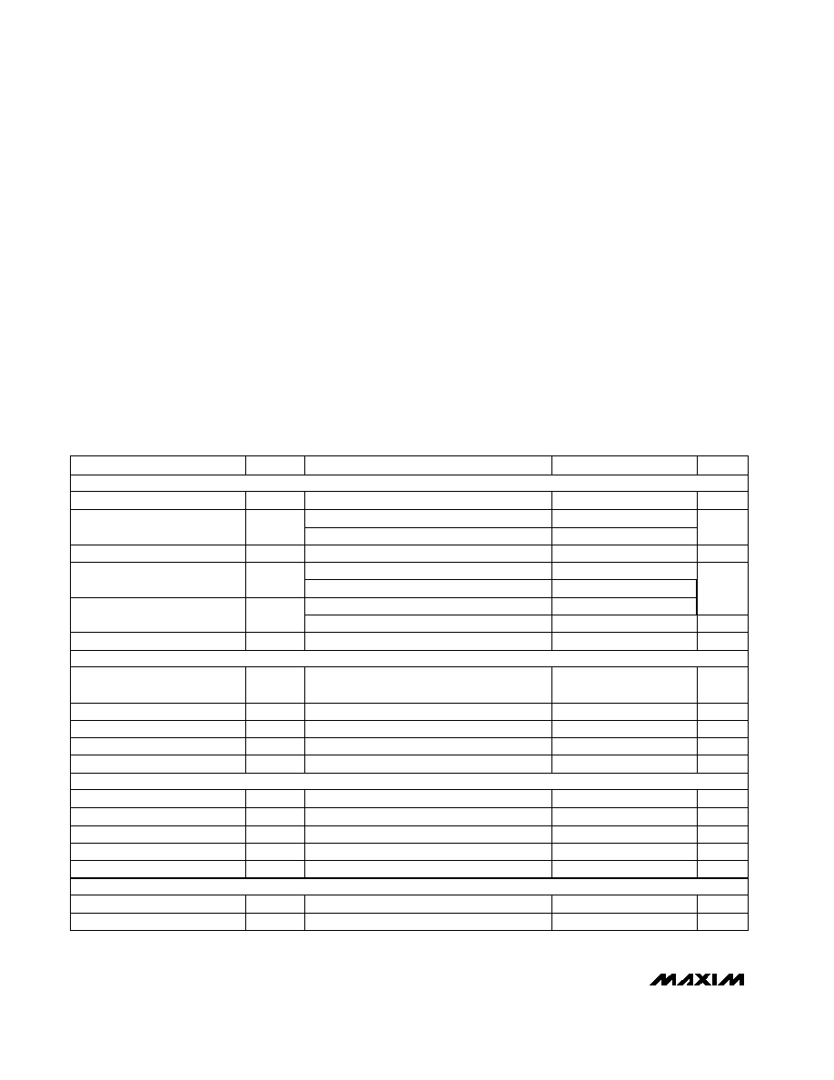
ELECTRICAL CHARACTERISTICS
(V
DD
= +2.7V to +5.25V; 73ksps; f
SCLK
= 2.1MHz (50% duty cycle); MAX1242--4.7µF capacitor at REF pin, MAX1243--external
reference; V
REF
= 2.5V applied to REF pin; T
A
= T
MIN
to T
MAX
; unless otherwise noted.)
V
DD
to GND .............................................................-0.3V to +6V
AIN to GND................................................-0.3V to (V
DD
+ 0.3V)
REF to GND ...............................................-0.3V to (V
DD
+ 0.3V)
Digital Inputs to GND...............................................-0.3V to +6V
DOUT to GND............................................-0.3V to (V
DD
+ 0.3V)
DOUT Current ..................................................................±25mA
Continuous Power Dissipation (T
A
= +70∞C)
Plastic DIP (derate 9.09mW/∞C above +70∞C) ...........727mW
SO (derate 5.88mW/∞C above +70∞C)........................471mW
CERDIP (derate 8.00mW/∞C above +70∞C)................640mW
Operating Temperature Ranges
MAX1242/MAX1243_C_A ..................................0∞C to +70∞C
MAX1242/MAX1243_E_ A ..............................-40∞C to +85∞C
MAX1242/MAX1243_MJA ............................-55∞C to +125∞C
Storage Temperature Range............................-60∞C to +150∞C
Lead Temperature (soldering, 10sec) ............................+300∞C
ABSOLUTE MAXIMUM RATINGS
Stresses beyond those listed under "Absolute Maximum Ratings" may cause permanent damage to the device. These are stress ratings only, and functional
operation of the device at these or any other conditions beyond those indicated in the operational sections of the specifications is not implied. Exposure to
absolute maximum rating conditions for extended periods may affect device reliability.
ANALOG INPUT
CONVERSION RATE
DYNAMIC SPECIFICATIONS
(10kHz sine-wave input, 0V to 2.5Vp-p, 73ksps, f
SCLK
= 2.1MHz)
DC ACCURACY
(Note 1)
MAX124_B
±2
Input Voltage Range
0
V
REF
V
Input Capacitance
Aperture Jitter
<50
ps
16
pF
MAX124_A
MAX124_B
MAX124_A
Aperture Delay
t
AP
30
ns
Figure 9
Track/Hold Acquisition Time
t
ACQ
1.5
µs
Throughput Rate
73
ksps
f
SCLK
= 2.1MHz
Conversion Time
PARAMETER
SYMBOL
MIN
TYP
MAX
UNITS
±1
Offset Error
LSB
Differential Nonlinearity
DNL
±1
LSB
±1.0
±2
Gain Error (Note 3)
±1
Resolution
10
Bits
Relative Accuracy (Note 2)
±0.5
LSB
t
CONV
5.5
7.5
µs
Small-Signal Bandwidth
Signal-to-Noise Plus
Distortion Ratio
SINAD
66
dB
2.25
MHz
Full-Power Bandwidth
Total Harmonic Distortion
THD
-70
dB
1.0
-3dB rolloff
MHz
CONDITIONS
Spurious-Free Dynamic Range
ppm/∞C
No missing codes over temperature
MAX124_B
±0.25
SFDR
70
Up to the 5th harmonic
dB
MAX124_A
LSB
DC ACCURACY
(Note1)
CONVERSION RATE
ANALOG INPUT
DYNAMIC SPECIFICATIONS
(10kHz sine-wave input, 0V to 2.5p-p, 73ksps, f
SCLK
=2.1MHz)
+2.7V to +5.25V, Low-Power, 10-Bit
Serial ADCs in SO-8
_______________________________________________________________________________________
3
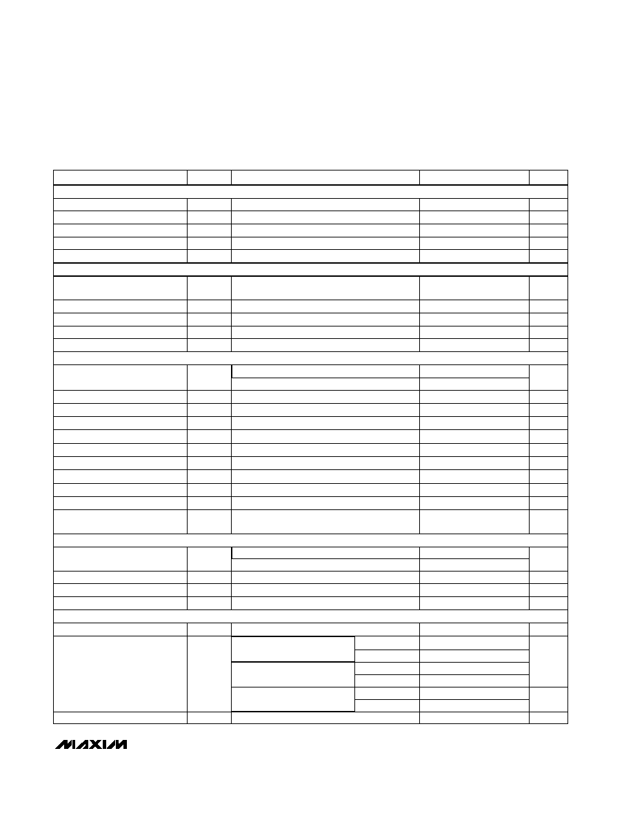
ELECTRICAL CHARACTERISTICS (continued)
(V
DD
= +2.7V to +5.25V; 73ksps; f
SCLK
= 2.1MHz (50% duty cycle); MAX1242--4.7µF capacitor at REF pin, MAX1243--external
reference; V
REF
= 2.5V applied to REF pin; T
A
= T
MIN
to T
MAX
; unless otherwise noted.)
Capacitive Bypass at REF
4.7
µF
Load Regulation (Note 5)
0.35
mV
0mA to 0.2mA output load
REF Temperature Coefficient
±30
ppm/∞C
MAX1242
REF Short-Circuit Current
30
mA
REF Output Voltage
2.470
2.500
2.530
V
T
A
= +25∞C (Note 4)
Power-Supply Rejection (Note 7)
PSR
V
DD
= V
DD(min)
to V
DD(max)
, full-scale input
1.00
V
DD
+
50mV
Supply Current
I
DD
3.0
0.8
V
DD
> 3.6V
I
SINK
= 16mA
Output Voltage High
SCLK, CS Input High Voltage
V
IH
2.0
V
SCLK, CS Input Low Voltage
Capacitive Bypass at REF
0.1
µF
V
IL
0.8
V
DD
3.6V
V
V
OH
V
DD
- 0.5
V
Three-State Leakage Current
I
L
±0.01
±10
I
SOURCE
= 0.5mA
µA
CS = V
DD
Three-State Output Capacitance
C
OUT
15
pF
CS = V
DD
(Note 6)
Output Voltage Low
V
OL
0.4
V
PARAMETER
SYMBOL
MIN
TYP
MAX
UNITS
I
SINK
= 5MA
SHDN Input Mid Voltage
V
SM
1.1
V
DD
- 1.1
V
SHDN Voltage, Floating
V
FLT
V
DD
/ 2
V
SHDN Max Allowed Leakage,
Mid Input
±100
SHDN = float
nA
SHDN = float
SCLK, CS Input Capacitance
Input Voltage Range
V
C
IN
15
pF
SHDN Input High Voltage
V
SH
V
DD
- 0.4
(Note 6)
V
SHDN Input Low Voltage
V
SL
0.4
V
Input Resistance
SHDN Input Current
±4.0
18
25
k
REF Input Current in Shutdown
µA
SHDN = 0V or V
DD
SCLK, CS Input Hysteresis
V
HYST
±0.01
10
µA
SHDN = 0V
CONDITIONS
Input Current
0.2
V
SCLK, CS Input Leakage
I
IN
±0.01
±1
100
150
µA
µA
V
IN
= 0V or V
DD
Operating mode (MAX1242)
V
DD
= 5.25V
Operating mode (MAX1243)
V
DD
= 5.25V
V
DD
= 3.6V
Power-down
V
DD
= 5.25V
V
DD
= 3.6V
Supply Voltage
V
DD
V
V
DD
= 3.6V
1.9
10
3.5
15
±0.3
1.6
2.5
0.9
1.5
1.8
3.0
1.4
2.0
2.7
5.25
mA
µA
mV
Operating mode (MAX1242)
EXTERNAL REFERENCE
(VREF = 2.5V)
INTERNAL REFERENCE
(MAX1242 only)
DIGITAL INPUTS: SCLK,
C
CS
S
,
S
SH
HD
DN
N
DIGITAL OUTPUT: DOUT
POWER REQUIREMENTS
MAX1242/MAX1243
+2.7V to +5.25V, Low-Power, 10-Bit
Serial ADCs in SO-8
4
_______________________________________________________________________________________
TIMING CHARACTERISTICS
(V
DD
= +2.7V to +5.25V, circuit of Figure 9, T
A
= T
MIN
to T
MAX
, unless otherwise noted.)
Note 1:
Tested at V
DD
= +2.7V.
Note 2:
Relative accuracy is the deviation of the analog value at any code from its theoretical value after the full-scale range and
offset have been calibrated.
Note 3:
Offset nulled.
Note 4:
Sample tested to 0.1% AQL.
Note 5:
External load should not change during conversion for specified accuracy.
Note 6:
Guaranteed by design. Not subject to production testing.
Note 7:
Measured as [V
FS
(V
DD(min)
) - V
FS
(V
DD(max)
)].
Note 8:
To guarantee acquisition time, t
ACQ
is the maximum time the device takes to acquire the signal, and is also the minimum
time needed for the signal to be acquired.
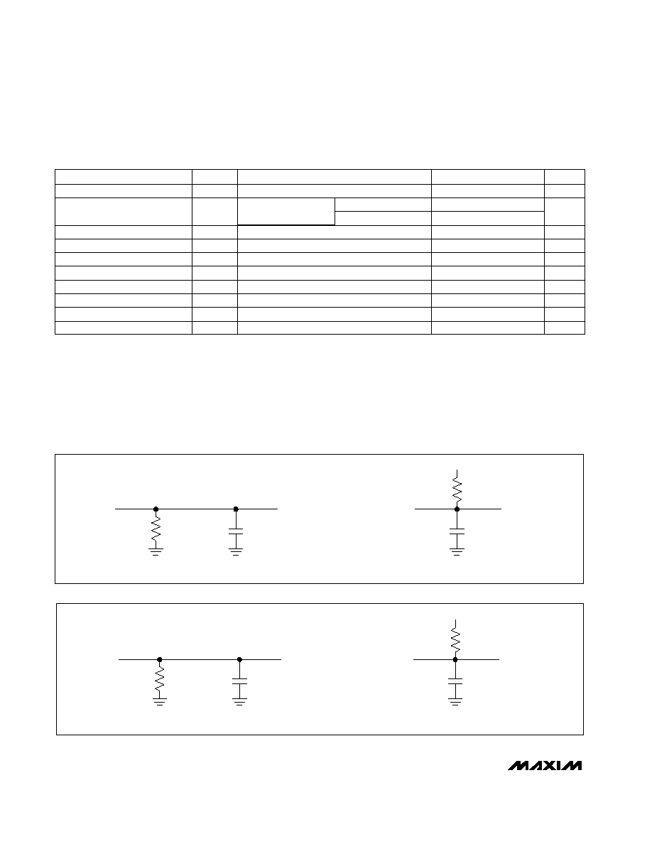
DOUT
DOUT
6k
DGND
C
LOAD
= 50pF
C
LOAD
= 50pF
6k
DGND
+2.7V
b) High-Z to V
OL
and V
OH
to V
OL
a) High-Z to V
OH
and V
OL
to V
OH
DOUT
DOUT
6k
DGND
C
LOAD
= 50pF
C
LOAD
= 50pF
6k
DGND
+2.7V
b) V
OL
to High-Z
a) V
OH
to High-Z
Figure 1. Load Circuits for DOUT Enable Time
Figure 2. Load Circuits for DOUT Disable Time
MAX124_ _M
MAX124_ _C/E
Figure 1, C
LOAD
= 50pF
Figure 1,
C
LOAD
= 50pF
CS = V
DD
(Note 8)
Figure 2, C
LOAD
= 50pF
CONDITIONS
ns
240
t
DV
CS Fall to Output Enable
ns
20
200
t
DO
µs
1.5
t
ACQ
Acquisition Time
SCLK Fall to Output Data Valid
ns
240
t
CS
CS Pulse Width
ns
0
t
STR
DOUT Rise to SCLK Rise (Note 6)
ns
50
t
CS0
SCLK Low to CS Fall Setup Time
ns
240
t
TR
CS Rise to Output Disable
MHz
0
2.1
f
SCLK
SCLK Clock Frequency
ns
200
t
CH
SCLK Pulse Width High
ns
200
t
CL
SCLK Pulse Width Low
UNITS
MIN
TYP
MAX
SYMBOL
PARAMETER
20
240
MAX1242/MAX1243
+2.7V to +5.25V, Low-Power, 10-Bit
Serial ADCs in SO-8
_______________________________________________________________________________________
5
2.00
0.50
2.25
2.75
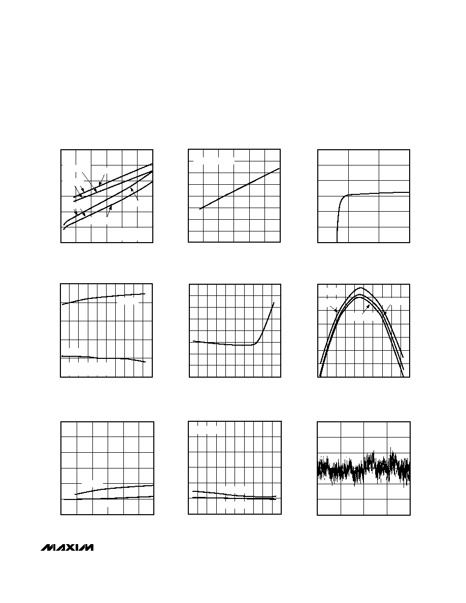
SUPPLY CURRENT
vs. SUPPLY VOLTAGE
1.75
1.25
1.50
1.00
0.75
SUPPLY VOLTAGE (V)
SUPPLY CURRENT (mA)
3.75
5.25
3.25
4.25
4.75
MAX1242/43-01
R
L
=
CODE = 1010101000
MAX1243
MAX1242
C
LOAD
= 20pF
C
LOAD
= 50pF
C
LOAD
= 50pF
C
LOAD
= 20pF
4.0
3.5
0
2.25
2.75
SHUTDOWN SUPPLY CURRENT
vs. SUPPLY VOLTAGE
3.0
2.5
1.5
2.0
1.0
0.5
SUPPLY VOLTAGE (V)
SHUTDOWN SUPPLY CURRENT (
µ
A)
3.75
5.25
3.25
4.25
4.75
MAX1242/43-02
MAX1242/MAX1243
2.5015
2.4985
2.25
INTERNAL REFERENCE VOLTAGE
vs. SUPPLY VOLTAGE
2.5000
2.5010
2.5005
2.4995
2.4990
SUPPLY VOLTAGE (V)
INTERNAL REFERENCE VOLTAGE (V)
3.75
2.75
3.25
MAX1242/43-03
MAX1242
0.8
0.9
1.0
1.1
1.2
1.3
-60
-20
20
60
100
140
SUPPLY CURRENT vs. TEMPERATURE
TEMPERATURE
(∞C)
SUPPLY CURRENT (mA)
MAX1242/43-04
MAX1243
MAX1242
R
LOAD
=
CODE = 1010101000
0
0.10
0.05
0.20
0.15
0.25
0.30
2.25
3.25
3.75
2.75
4.25
4.75
5.25
INTEGRAL NONLINEARITY
vs. SUPPLY VOLTAGE
MAX1242/43-07
SUPPLY VOLTAGE (V)
INL (LSB)
MAX1242
MAX1243
1.00
1.50
1.25
1.75
2.25
2.00
2.75
2.50
3.00
-60
-20
20
60
100
140
SHUTDOWN CURRENT
vs. TEMPERATURE
TEMPERATURE
(∞C)
SHUTDOWN CURRENT (
µ
A)
MAX1242/43-05
2.494
2.495
2.496
2.497
2.498
2.499
2.500
2.501
-60
-20
-40
20
0
60
40
100 120
80
140
INTERNAL REFERENCE VOLTAGE
vs. TEMPERATURE
TEMPERATURE
(∞C)
INTERNAL REFERENCE VOLTAGE (V)
MAX1242/43-06
V
DD
= 2.7V
V
DD
= 5V
V
DD
= 3.6V
MAX1242
0
0.15
0.10
0.05
0.20
0.25
0.30
-60
20
0
-40 -20
40 60 80 100 120 140
INTEGRAL NONLINEARITY
vs. TEMPERATURE
MAX1242/43-08
TEMPERATURE (∞C)
INL (LSB)
V
DD
= 2.7V
MAX1242
MAX1243
0.15
INTEGRAL NONLINEARITY
vs. CODE
-0.15
0
-0.05
-0.10
0.10
0.05
MAX1242/43-09
INL (LSB)
CODE
256
512
768
1024
0
__________________________________________Typical Operating Characteristics
(V
DD
= +3.0V, V
REF
= 2.5V, f
SCLK
= 2.1MHz, C
LOAD
= 20pF, T
A
= +25∞C, unless otherwise noted.)