_______________General Description
The MAX1247 evaluation kit (EV kit) is an assembled
and tested surface-mount PC board that demonstrates
the 3V, 12-bit, 4-channel MAX1247 analog-to-digital
converter.
The MAX1247 evaluation system (EV system) is a com-
plete, low-cost, 4-channel data-acquisition system con-
sisting of a MAX1247 EV kit and a Maxim 3V microcon-
troller (µC) module. IBM PC-compatible software pro-
vides a handy user interface to exercise the MAX1247's
features. Source code is provided.
The MAX1246 EV kit and EV system are identical to the
MAX1247 EV kit and EV system except that the
MAX1247 is replaced by the MAX1246, which has an
internal 2.5V reference.
Order the EV system for comprehensive evaluation of
the MAX1247 or MAX1246 using a personal computer.
Order the EV kit if you have already purchased the 3V
µC module with a previous Maxim EV system, or for
custom use in other µC-based systems.
____________________________Features
o
Proven PC Board Layout
o
Complete Evaluation System
o
Convenient On-Board Test Points
o
Data-Logging Software
o
Source Code Provided
o
Fully Assembled and Tested
_______________Stand-Alone EV Kits
The MAX1246/MAX1247 EV kit provides a proven PC
board layout to facilitate evaluation of the MAX1246 or
MAX1247. It must be interfaced to appropriate timing
signals for proper operation. Refer to the MAX1246/
MAX1247 data sheet for timing requirements.
Systems that have 5V as well as 3V logic must provide
level translation for the MAX1246/MAX1247 DOUT and
SSTRB outputs. No level translation is necessary on the
digital interface inputs.
Evaluate: MAX1246/MAX1247
MAX1246/MAX1247 Evaluation Systems
________________________________________________________________
Maxim Integrated Products
1
19-1161; Rev 1; 6/97
QTY
DESCRIPTION
C1, C7≠C10
5
C2, C4, C6,
C11
4
C13
1
0.1µF ceramic surface-mount capacitor
(MAX1247 EV kit only)
C5
1
C12
1
0.047µF ceramic surface-mount capacitor
(MAX1247 EV kit only)
H1
1
J1
1
JU1, JU2,
JU5, JU6
4
R1≠R4
4
1k
, 5% surface-mount resistors
10µF surface-mount tantalum capacitor
0.1µF ceramic surface-mount capacitors
0.01µF ceramic surface-mount capacitors
DESIGNATION
10-pin header
2 x 20 header
2-pin headers
MAX1246/MAX1247 EV Kits
___________________ Component List
______________Ordering Information
R5
1
100
, 5% surface-mount resistor
R6, R7
2
1M
, 5% surface-mount resistors
U1
1
MAX1247BCEE or MAX1246BCEE
QTY
DESCRIPTION
1
MAX1246EVKIT-QSOP
1
68L11D
µ
C MODULE (68L11D MODULE)
U2
1
MAX872CSA (MAX1247 EV kit only)
U3
1
MAX393CSE
U4
1
MAX495CSA
None
1
Printed circuit board
MAX1246EVL11
____________________Component List
PART
TEMP. RANGE
PIN-PACKAGE
MAX1246
EVKIT-QSOP
0∞C to +70∞C
Surface Mount
MAX1246EVL11-QSOP
0∞C to +70∞C
Surface Mount
MAX1247
EVKIT-QSOP
0∞C to +70∞C
Surface Mount
MAX1247EVL11-QSOP
0∞C to +70∞C
Surface Mount
C3
1
4.7µF surface-mount tantalum capacitor
QTY
DESCRIPTION
1
MAX1247EVKIT-QSOP
1
68L11D
µ
C MODULE (68L11D MODULE)
MAX1247EVL11
____________________Component List
For free samples & the latest literature: http://www.maxim-ic.com, or phone 1-800-998-8800.
For small orders, phone 408-737-7600 ext. 3468.

Evaluate: MAX1246/MAX1247
MAX1246/MAX1247 Evaluation Systems
2
_______________________________________________________________________________________
__________ EV Systems Quick Start
A single program, "MAX1247", is used for both the
MAX1246 and the MAX1247 EV systems.
1) Copy the files from the distribution disk to your hard
disk or to blank floppy disks. The EV kit software
should be in its own directory. The necessary files
are in the distribution disk's root directory, and the
source code is in the SOURCE subdirectory. The
SOURCE subdirectory is not required to operate
the EV kit.
2) Make sure that the jumpers are configured accord-
ing to Table 1. Table 2 lists the functions associated
with each jumper.
3) Carefully connect the boards by aligning the
EV kit's 40-pin header with the µC module's
40-pin connector. Gently press them together. The
two boards should be flush against each other.
4) Connect a 5V DC power source (16V max) to the
µC module at the terminal block located next to the
on/off switch, in the upper-right corner of the µC
module. Observe the polarity marked on the board.
5) Connect a cable from the computer's serial port to
the µC module. If using a 9-pin serial port, use a
straight-through, 9-pin, female-to-male cable. If the
only available serial port uses a 25-pin connector, a
standard 25-pin to 9-pin adapter is required. The
EV kit software checks the modem status lines
(CTS, DSR, DCD) to confirm that the correct port
has been selected.
6) Start the software on the IBM PC by setting the cur-
rent directory to match the directory that contains
the Maxim programs, and then type the program
name "MAX1247" (for the MAX1246, type
"MAX1247 FASTPD"
). Do not turn off or discon-
nect the
µ
C module while the program is running; if
you do, you will have to restart the program.
7) The program will ask which port the µC module is
connected to. Press the space bar until the correct
PC serial port is highlighted, then press ENTER.
The program will be in terminal-emulation mode.
8) Turn on the power for the
µ
C module. The
µ
C mod-
ule will display its logon banner and test its RAM.
9) Download and run the RAM resident program on
the
µ
C module by pressing ALT+L (i.e., hold down
the ALT key as you strike the L key). The program
will prompt you for the file name. Press the ENTER
key to download and run the file.
10) Press ALT+C to switch to the Control Panel screen
after the RAM resident program has been success-
fully downloaded.
11) Apply input signals to CH0≠CH3 on the EV board.
Observe the readout on the screen. Table 3 lists the
commands that are available from the control panel
screen.
12) Before turning off power to the EV kit, exit the pro-
gram by pressing ALT+X.
Table 1. Default Jumper Settings
JUMPER
MAX1246
JUMPER
STATE
FUNCTION
JU1
Closed
Drive SHDN pin
JU2
Open
See Table 2
JU3
Closed
(trace)
Bypass
supply-current
measurement
JU4
Closed
(trace)
Drive COM pin
JU5
Open
See Table 2
JU6
Open
VREF not connected
to V
DD
MAX1247
JUMPER
STATE
Closed
Closed
Closed
(trace)
Closed
(trace)
Closed
Open

JU2
Evaluate: MAX1246/MAX1247
MAX1246/MAX1247 Evaluation Systems
_______________________________________________________________________________________
3
JUMPER
STATE
FUNCTION
Closed
Drive SHDN pin with pin 34 of the µC module.
JU1
Open
Force SHDN to float.
Closed
REFADJ = V
DD
. Disable the internal reference buffer (see JU5 and JU6 settings).
JU2
Open
REFADJ = Open. Enable the internal reference buffer. Refer to the MAX1246/MAX1247 data sheet for
additional information.
Closed
Current-sense jumper (in series with V
DD
)
JU3
Open
Closed
Drive the COM pin with buffer U4.
JU4
Open
COM disconnected from U4; COM must be driven directly by the user.
Closed
VREF = MAX872 reference (MAX872 not supplied with MAX1246 EV kit).
JU5*
Open
MAX872 disconnected from the MAX1247's VREF input.
Closed
VREF = V
DD
JU6*
Open
V
DD
disconnected from the VREF input.
Do not operate the kit with JU3 open. Supply current may be measured by cutting JU3 open and
connecting a current meter across JU3.
Table 2. Jumper Settings
Detailed Description
________________________of Hardware
The MAX872 is a micropower 2.5V reference supplied
with the MAX1247 EV kit.
The MAX495 is a low-voltage Rail-to-Rail
Æ
op amp with
a 500kHz gain-bandwidth product. The MAX495
buffers the external COM input source.
The MAX393 analog switch allows the EV kit software to
route the MAX1246/MAX1247 COM pin to ground or to
the external COM input. In addition, the external COM
input can be routed to input channel 0. Typical systems
connect COM directly to analog ground or the analog
common voltage.
Changing the Reference Voltage
To supply a different external reference, open JU2 and
apply the reference voltage between VREF and GND or
J10 (REFADJ) and GND. Refer to the MAX1246/
MAX1247 data sheet for additional information.
Input Filtering
The EV kit has an RC filter on each input with a time
constant (
) of 10µs. The MAX1246/MAX1247's acquisi-
tion time with a 1MHz clock is 3µs.
The RC filter's settling time may increase the acquisi-
tion time required for full accuracy when switching
input channels.
Detailed Description
________________________of Software
The software allows all features of the MAX1246/
MAX1247 to be exercised. Refer to Tables 3 and 4 for a
complete listing of available features.
The EV kit default software program ("KIT1247.L11")
that is loaded into the 68L11D module operates at a
throughput rate of 6.41ksps. For faster throughput,
download the program "FAST1247.L11" at step 9 of the
Quick Start section. This program has a throughput rate
of approximately 13ksps.
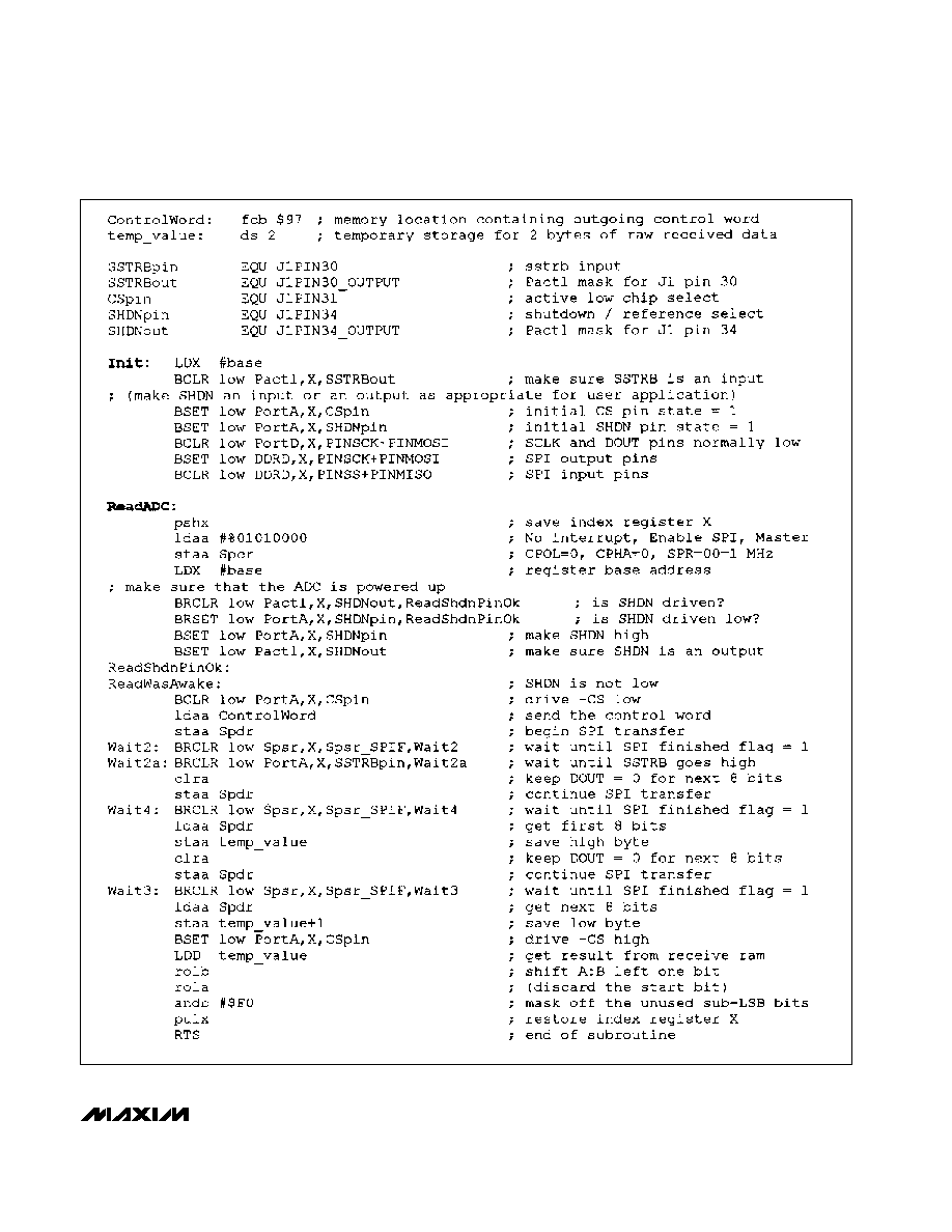
Listing 1 shows an example of interfacing the MAX1246/
MAX1247 to the 68HC11 processor.
*Note: Jumpers JU5 and JU6 should not both be closed.
Rail-to-Rail is a registered trademark of Nippon Motorola Ltd.

Evaluate: MAX1246/MAX1247
MAX1246/MAX1247 Evaluation Systems
4
_______________________________________________________________________________________
Table 4. Command-Line Options
when Starting Software
Table 3. Command Reference
KEY
FUNCTION
0, 1, 2, 3
P
Power-up delay. Timing is approximate and should be verified with an oscilloscope. When using an external refer-
ence, power-up delay is not necessary and should be set to zero. Power-up delay is used regardless of which
power-cycling mode is selected.
Enables or disables the corresponding input channel 0, 1, 2, or 3. The EV kit software scans all enabled channels.
O
Oscilloscope demo. Samples are collected and discarded as fast as possible. Observe waveforms and timing with
an oscilloscope.
F3
L
Enables or disables data logging. If the -L command-line option was not specified, the L command prompts for a
log-file name.
Writes a marker into the data-log file.
D
Delay between samples. Delays longer than one second are handled by the IBM PC; otherwise, the µC module
handles the delay. Timing is approximate and should be verified with an oscilloscope.
F4
Measures the value of a user-applied COM voltage.
F5
Changes the assumed value of VREF.
C
Displays the conversion results in decimal form.
F6
S
Samples one of the four inputs at high speed. The sampling rate is controlled by the P and D delays. Due to pro-
gram overhead, the O and S commands operate at different rates. Timing should be verified with an oscilloscope.
Changes the assumed voltage at COM. Selecting G connects the COM pin to ground; selecting E connects the
COM pin to the EXTCOM input pad.
V
Displays the conversion results in volts.
F7
Internal clock mode
F8
External clock mode
F1
Selects input scale (unipolar, bipolar, unipolar differential, bipolar differential) for all enabled channels. Disabled
channels are unaffected.
ALT+T
Switches back to terminal mode.
ALT+X
Exits to DOS.
Selects power-down mode.
COMMAND
FUNCTION
COM
vvv
2
Defaults to COM2 PC serial port.
Specifies the voltage at the COM pin.
MONO
For use with monochrome or LCD
display.
?
FASTPD
Enables the fast power-down mode
for the MAX1246.
Lists command-line options.
VREF
vvv
Specifies the actual measured volt-
age at the VREF pin (nominally 2.5V).
-L
filename
Opens file
filename for data logging
and enables the data-logging
commands.
,
1
Defaults to COM1 PC serial port.
Evaluate: MAX1246/MAX1247
MAX1246/MAX1247 Evaluation Systems
_______________________________________________________________________________________
5
Listing 1. Reading the MAX1246/MAX1247 with the 68HC11/68L11 SPI Interface