
General Description
The MAX12528 is a dual 80Msps, 12-bit analog-to-digi-
tal converter (ADC) featuring fully differential wideband
track-and-hold (T/H) inputs, driving internal quantizers.
The MAX12528 is optimized for low power, small size,
and high dynamic performance in intermediate frequen-
cy (IF) and baseband sampling applications. This dual
ADC operates from a single 3.3V supply, consuming
only 726mW while delivering a typical 69.8dB signal-to-
noise ratio (SNR) performance at a 175MHz input fre-
quency. The T/H input stages accept single-ended or
differential inputs up to 400MHz. In addition to low oper-
ating power, the MAX12528 features a 330µW power-
down mode to conserve power during idle periods.
A flexible reference structure allows the MAX12528 to
use the internal 2.048V bandgap reference or accept
an externally applied reference and allows the refer-
ence to be shared between the two ADCs. The refer-
ence structure allows the full-scale analog input range
to be adjusted from ±0.35V to ±1.15V. The MAX12528
provides a common-mode reference to simplify design
and reduce external component count in differential
analog input circuits.
The MAX12528 supports either a single-ended or differ-
ential input clock. User-selectable divide-by-two (DIV2)
and divide-by-four (DIV4) modes allow for design flexibil-
ity and help eliminate the negative effects of clock jitter.
Wide variations in the clock duty cycle are compensated
with the ADC's internal duty-cycle equalizer (DCE).
The MAX12528 features two parallel, 12-bit-wide,
CMOS-compatible outputs. The digital output format is
pin-selectable to be either two's complement or Gray
code. A separate power-supply input for the digital out-
puts accepts a 1.7V to 3.6V voltage for flexible interfac-
ing with various logic levels. The MAX12528 is available
in a 10mm x 10mm x 0.8mm, 68-pin thin QFN package
with exposed paddle (EP), and is specified for the
extended (-40
∞C to +85∞C) temperature range.
Applications
IF and Baseband Communication Receivers
Cellular, LMDS, Point-to-Point Microwave,
MMDS, HFC, WLAN
I/Q Receivers
Medical Imaging
Portable Instrumentation
Digital Set-Top Boxes
Low-Power Data Acquisition
Features
Direct IF Sampling Up to 400MHz
Excellent Dynamic Performance
70.7dB/69.8dB SNR at f
IN
= 70MHz/175MHz
78.2dBc/72.9dBc SFDR at f
IN
= 70MHz/175MHz
3.3V Low-Power Operation
760mW (Differential Clock Mode)
726mW (Single-Ended Clock Mode)
Fully Differential or Single-Ended Analog Input
Adjustable Differential Analog Input Voltage
750MHz Input Bandwidth
Internal, External, or Shared Reference
Differential or Single-Ended Clock
Accepts 25% to 75% Clock Duty Cycle
User-Selectable DIV2 and DIV4 Clock Modes
Power-Down Mode
CMOS Outputs in Two's Complement or Gray
Code
Out-of-Range and Data-Valid Indicators
Compact, 68-Pin Thin QFN Package (10mm x
10mm x 0.8mm)
Evaluation Kit Available (Order MAX12528EVKIT)
MAX12528
Dual, 80Msps, 12-Bit, IF/Baseband ADC
________________________________________________________________ Maxim Integrated Products
1
Ordering Information
19-3643; Rev 0; 4/05
For pricing, delivery, and ordering information, please contact Maxim/Dallas Direct! at
1-888-629-4642, or visit Maxim's website at www.maxim-ic.com.
EVALUATION KIT
AVAILABLE
PART
TEMP RANGE
PIN-PACKAGE
PKG
CODE
MAX12528ETK
-40
∞C to +85∞C 68 Thin QFN-EP* T6800-2
Pin Configuration appears at end of data sheet.
*EP = Exposed paddle.
Selector Guide
PART
SAMPLING RATE
(Msps)
RESOLUTION
(Bits)
MAX12528
80
12
MAX12557
65
14
MAX12527
65
12
MAX12528
Dual, 80Msps, 12-Bit, IF/Baseband ADC
2
_______________________________________________________________________________________
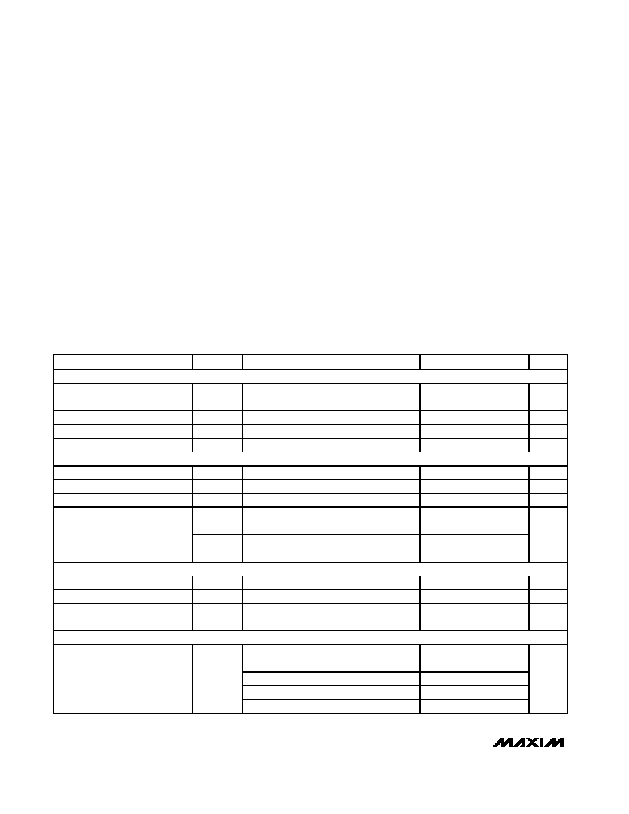
ABSOLUTE MAXIMUM RATINGS
ELECTRICAL CHARACTERISTICS
(V
DD
= 3.3V, OV
DD
= 2.0V, GND = 0, REFIN = REFOUT (internal reference), C
L
10pF at digital outputs, A
IN
= -0.5dBFS (differen-
tial), DIFFCLK/SECLK = OV
DD
, PD = GND, SHREF = GND, DIV2 = GND, DIV4 = GND, G/T = GND, f
CLK
= 80MHz, T
A
= -40∞C to
+85∞C, unless otherwise noted. Typical values are at T
A
= +25∞C.) (Note 1)
Stresses beyond those listed under "Absolute Maximum Ratings" may cause permanent damage to the device. These are stress ratings only, and functional
operation of the device at these or any other conditions beyond those indicated in the operational sections of the specifications is not implied. Exposure to
absolute maximum rating conditions for extended periods may affect device reliability.
V
DD
to GND ................................................................-0.3V to +3.6V
OV
DD
to GND............-0.3V to the lower of (V
DD
+ 0.3V) and +3.6V
INAP, INAN to GND ...-0.3V to the lower of (V
DD
+ 0.3V) and +3.6V
INBP, INBN to GND ...-0.3V to the lower of (V
DD
+ 0.3V) and +3.6V
CLKP, CLKN to
GND ........................-0.3V to the lower of (V
DD
+ 0.3V) and +3.6V
REFIN, REFOUT
to GND ..................-0.3V to the lower of (V
DD
+ 0.3V) and +3.6V
REFAP, REFAN,
COMA to GND ......-0.3V to the lower of (V
DD
+ 0.3V) and +3.6V
REFBP, REFBN,
COMB to GND ......-0.3V to the lower of (V
DD
+ 0.3V) and +3.6V
DIFFCLK/SECLK, G/T, PD, SHREF, DIV2,
DIV4 to GND .........-0.3V to the lower of (V
DD
+ 0.3V) and +3.6V
D0A≠D11A, D0B≠D11B, DAV,
DORA, DORB to GND..............................-0.3V to (OV
DD
+ 0.3V)
Continuous Power Dissipation (T
A
= +70∞C)
68-Pin Thin QFN 10mm x 10mm x 0.8mm
(derate 70mW/∞C above +70∞C) ....................................4000mW
Thermal Resistance
jc........................................................0.4∞C/W
Operating Temperature Range................................-40∞C to +85∞C
Junction Temperature ...........................................................+150∞C
Storage Temperature Range .................................-65∞C to +150∞C
Lead Temperature (soldering, 10s)......................................+300∞C
PARAMETER
SYMBOL
CONDITIONS
MIN
TYP
MAX
UNITS
DC ACCURACY
Resolution
12
Bits
Integral Nonlinearity
INL
f
IN
= 3MHz
±0.6
±1.6
LSB
Differential Nonlinearity
DNL
f
IN
= 3MHz, no missing codes
±0.3
±0.85
LSB
Offset Error
±0.1
±0.7
%FSR
Gain Error
±0.5
±4.3
%FSR
ANALOG INPUT (INAP, INAN, INBP, INBN)
Differential Input Voltage Range
V
DIFF
Differential or single-ended inputs
±1.024
V
Common-Mode Input Voltage
V
DD
/ 2
V
Analog Input Resistance
R
IN
Each input (Figure 3)
2
k
C
PAR
Fixed capacitance to ground,
each input (Figure 3)
2
Analog Input Capacitance
C
SAMPLE
Switched capacitance,
each input (Figure 3)
4.5
pF
CONVERSION RATE
Maximum Clock Frequency
f
CLK
80
MHz
Minimum Clock Frequency
5
MHz
Data Latency
Figure 5
8
Clock
Cycles
DYNAMIC CHARACTERISTICS
Small-Signal Noise Floor
SSNF
Input at -35dBFS
71.0
72.1
dBFS
f
IN
= 3MHz at -0.5dBFS
69.3
71.2
f
IN
= 40MHz at -0.5dBFS
70.7
f
IN
= 70MHz at -0.5dBFS
70.7
Signal-to-Noise Ratio
SNR
f
IN
= 175MHz at -0.5dBFS
67.1
69.8
dB
MAX12528
Dual, 80Msps, 12-Bit, IF/Baseband ADC
_______________________________________________________________________________________
3
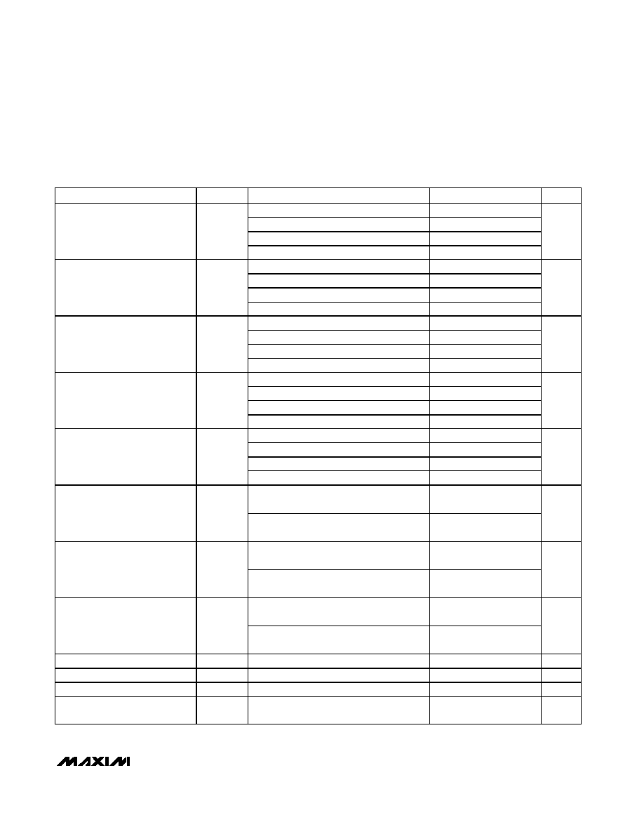
ELECTRICAL CHARACTERISTICS (continued)
(V
DD
= 3.3V, OV
DD
= 2.0V, GND = 0, REFIN = REFOUT (internal reference), C
L
10pF at digital outputs, A
IN
= -0.5dBFS (differen-
tial), DIFFCLK/SECLK = OV
DD
, PD = GND, SHREF = GND, DIV2 = GND, DIV4 = GND, G/T = GND, f
CLK
= 80MHz, T
A
= -40∞C to
+85∞C, unless otherwise noted. Typical values are at T
A
= +25∞C.) (Note 1)
PARAMETER
SYMBOL
CONDITIONS
MIN
TYP
MAX
UNITS
f
IN
= 3MHz at -0.5dBFS
68.9
70.8
f
IN
= 40MHz at -0.5dBFS
70.2
f
IN
= 70MHz at -0.5dBFS
69.6
Signal-to-Noise Plus Distortion
SINAD
f
IN
= 175MHz at -0.5dBFS
64.6
67.7
dB
f
IN
= 3MHz at -0.5dBFS
74.7
85.6
f
IN
= 40MHz at -0.5dBFS
81.8
f
IN
= 70MHz at -0.5dBFS
78.2
Spurious-Free Dynamic Range
SFDR
f
IN
= 175MHz at -0.5dBFS
67.2
72.9
dBc
f
IN
= 3MHz at -0.5dBFS
-84.2
-73.3
f
IN
= 40MHz at -0.5dBFS
-79.3
f
IN
= 70MHz at -0.5dBFS
-75.8
Total Harmonic Distortion
THD
f
IN
= 175MHz at -0.5dBFS
-71.9
-66.4
dBc
f
IN
= 3MHz at -0.5dBFS
-87.2
f
IN
= 40MHz at -0.5dBFS
-85.2
f
IN
= 70MHz at -0.5dBFS
-85
Second Harmonic
HD2
f
IN
= 175MHz at -0.5dBFS
-81.5
dBc
f
IN
= 3MHz at -0.5dBFS
-92.1
f
IN
= 40MHz at -0.5dBFS
-85.5
f
IN
= 70MHz at -0.5dBFS
-78.2
Third Harmonic
HD3
f
IN
= 175MHz at -0.5dBFS
-72.9
dBc
f
IN1
= 68.5MHz at -7dBFS
f
IN2
= 71.5MHz at -7dBFS
-77.5
Two-Tone Intermodulation
Distortion (Note 2)
TTIMD
f
IN1
= 172.5MHz at -7dBFS
f
IN2
= 177.5MHz at -7dBFS
-72.8
dBc
f
IN1
= 68.5MHz at -7dBFS
f
IN2
= 71.5MHz at -7dBFS
-78.6
3rd-Order Intermodulation
Distortion
IM3
f
IN1
= 172.5MHz at -7dBFS
f
IN2
= 177.5MHz at -7dBFS
-74.3
dBc
f
IN1
= 68.5MHz at -7dBFS
f
IN2
= 71.5MHz at -7dBFS
78.6
Two-Tone Spurious-Free
Dynamic Range
SFDR
TT
f
IN1
= 172.5MHz at -7dBFS
f
IN2
= 177.5MHz at -7dBFS
74.3
dBc
Full-Power Bandwidth
FPBW
Input at -0.2dBFS, -3dB rolloff
750
MHz
Aperture Delay
t
AD
Figure 5
1.2
ns
Aperture Jitter
t
AJ
<0.15
ps
RMS
Output Noise
n
OUT
INAP = INAN = COMA
INBP = INBN = COMB
0.3
LSB
RMS

MAX12528
Dual, 80Msps, 12-Bit, IF/Baseband ADC
4
_______________________________________________________________________________________
ELECTRICAL CHARACTERISTICS (continued)
(V
DD
= 3.3V, OV
DD
= 2.0V, GND = 0, REFIN = REFOUT (internal reference), C
L
10pF at digital outputs, A
IN
= -0.5dBFS (differen-
tial), DIFFCLK/SECLK = OV
DD
, PD = GND, SHREF = GND, DIV2 = GND, DIV4 = GND, G/T = GND, f
CLK
= 80MHz, T
A
= -40∞C to
+85∞C, unless otherwise noted. Typical values are at T
A
= +25∞C.) (Note 1)
PARAMETER
SYMBOL
CONDITIONS
MIN
TYP
MAX
UNITS
Overdrive Recovery Time
±10% beyond full scale
1
Clock
cycle
INTERCHANNEL CHARACTERISTICS
f
INA
or f
INB
= 70MHz at -0.5dBFS
90
Crosstalk Rejection
f
INA
or f
INB
= 175MHz at -0.5dBFS
85
dB
Gain Matching
±0.01
±0.1
dB
Offset Matching
±0.01
%FSR
INTERNAL REFERENCE (REFOUT)
REFOUT Output Voltage
V
REFOUT
1.995
2.048
2.075
V
REFOUT Load Regulation
-1mA < I
REFOUT
< +1mA
35
mV/mA
REFOUT Temperature Coefficient
TC
REF
65
ppm/∞C
Short to V
DD
--sinking
0.24
REFOUT Short-Circuit Current
Short to GND--sourcing
2.1
mA
BUFFERED REFERENCE MODE (REFIN is driven by REFOUT or an external 2.048V single-ended reference source;
V
REFAP
/V
REFAN
/V
COMA
and V
REFBP
/V
REFBN
/V
COMB
are generated internally)
REFIN Input Voltage
V
REFIN
2.048
V
REFIN Input Resistance
R
REFIN
>50
M
COM_ Output Voltage
V
COMA
V
COMB
V
DD
/ 2
1.60
1.65
1.70
V
REF_P Output Voltage
V
REFAP
V
REFBP
V
DD
/ 2 + (V
REFIN
x 3/8)
2.418
V
REF_N Output Voltage
V
REFAN
V
REFBN
V
DD
/ 2 - (V
REFIN
x 3/8)
0.882
V
Differential Reference Voltage
V
REFA
V
REFB
V
REFA
= V
REFAP
- V
REFAN
V
REFB
= V
REFBP
- V
REFBN
1.440
1.536
1.590
V
Differential Reference
Temperature Coefficient
TC
REF
30
ppm/∞C
UNBUFFERED EXTERNAL REFERENCE (REFIN = GND, V
REFAP
/V
REFAN
/V
COMA
and V
REFBP
/V
REFBN
/V
COMB
are applied
externally, V
COMA
= V
COMB
= V
DD
/ 2)
REF_P Input Voltage
V
REFAP
V
REFBP
V
REF_P
- V
COM
+0.768
V
REF_N Input Voltage
V
REFAN
V
REFBN
V
REF_N
- V
COM
-0.768
V
COM_ Input Voltage
V
COM
V
DD
/ 2
1.65
V
Differential Reference Voltage
V
REFA
V
REFB
V
REF_
= V
REF_P
- V
REF_N
= V
REFIN
x 3/4
1.536
V

MAX12528
Dual, 80Msps, 12-Bit, IF/Baseband ADC
_______________________________________________________________________________________
5
ELECTRICAL CHARACTERISTICS (continued)
(V
DD
= 3.3V, OV
DD
= 2.0V, GND = 0, REFIN = REFOUT (internal reference), C
L
10pF at digital outputs, A
IN
= -0.5dBFS (differen-
tial), DIFFCLK/SECLK = OV
DD
, PD = GND, SHREF = GND, DIV2 = GND, DIV4 = GND, G/T = GND, f
CLK
= 80MHz, T
A
= -40∞C to
+85∞C, unless otherwise noted. Typical values are at T
A
= +25∞C.) (Note 1)
PARAMETER
SYMBOL
CONDITIONS
MIN
TYP
MAX
UNITS
REF_P Sink Current
I
REFAP
I
REFBP
V
REF_P
= 2.418V
1.2
mA
REF_N Source Current
I
REFAN
I
REFBN
V
REF_N
= 0.882V
0.85
mA
COM_ Sink Current
I
COMA
I
COMB
V
COM_
= 1.65V
0.85
mA
REF_P, REF_N Capacitance
C
REF_P
,
C
REF_N
13
pF
COM_ Capacitance
C
COM_
6
pF
CLOCK INPUTS (CLKP, CLKN)
Single-Ended Input High
Threshold
V
IH
DIFFCLK/SECLK = GND, CLKN = GND
0.8 x
V
DD
V
Single-Ended Input Low
Threshold
V
IL
DIFFCLK/SECLK = GND, CLKN = GND
0.2 x
V
DD
V
Minimum Differential Clock Input
Voltage Swing
DIFFCLK/SECLK = OV
DD
0.2
V
P-P
Differential Input Common-Mode
Voltage
DIFFCLK/SECLK = OV
DD
V
DD
/ 2
V
CLK_ Input Resistance
R
CLK
Each input (Figure 4)
5
k
CLK_ Input Capacitance
C
CLK
Each input
2
pF
DIGITAL INPUTS (DIFFCLK/
SECLK, G/T, PD, DIV2, DIV4)
Input High Threshold
V
IH
0.8 x
OV
DD
V
Input Low Threshold
V
IL
0.2 x
OV
DD
V
OV
DD
applied to input
±5
Input Leakage Current
Input connected to ground
±5
µA
Digital Input Capacitance
C
DIN
5
pF
DIGITAL OUTPUTS (D0A≠D11A, D0B≠D11B, DORA, DORB, DAV)
D0A≠D11A, D0B≠D11B, DORA, DORB:
I
SINK
= 200µA
0.2
Output-Voltage Low
V
OL
DAV: I
SINK
= 600µA
0.2
V
D0A≠D11A, D0B≠D11B, DORA, DORB:
I
SOURCE
= 200µA
OV
DD
-
0.2
Output-Voltage High
V
OH
DAV: I
SOURCE
= 600µA
OV
DD
-
0.2
V
OV
DD
applied to input
±5
Three-State Leakage Current
(Note 3)
I
LEAK
Input connected to ground
±5
µA