
SCOPE: BATTERY MANAGER
Device Type Generic Number SMD Number
01
MAX1259MJE/883B 5962-9326401MEA
01 MAX1259MLP/883B 5962-9326401M2C
Case Outline(s). The case outlines shall be designated in Mil-Std-1835 and as follows:
Outline Letter Mil-Std-1835 Case Outline Package Code
MAXIM SMD
JE E
GDIP1-T16 or CDIP2-T16 16 LEAD CERDIP J16
LP 2 CQCC1-N20 20 Pin Ceramic LCC L20
Absolute Maximum Ratings
Voltage to Any Pin Relative to GND ............................................................... -0.3V to +7V
Lead Temperature (soldering, 10 seconds) ................................................................ +300
∞
C
Storage Temperature .................................................................................. -65
∞
C to +150
∞
C
Continuous Power Dissipation ..............................................................................T
A
=
+
70
∞
C
16 lead CERDIP(derate 10.0mW/
∞
C above +70
∞
C) ................................................ 800mW
20 lead LCC(derate 9.1mW/
∞
C above +70
∞
C) ........................................................ 727mW
Junction Temperature T
J
....................................................................................... +150
∞
C
Thermal Resistance, Junction to Case,
JC:
Case Outline 16 lead CERDIP .................................................................. 50
∞
C/W
Case Outline 20 lead LCC ......................................................................... 20
∞
C/W
Thermal Resistance, Junction to Ambient,
JA:
Case Outline 16 lead CERDIP ................................................................ 100
∞
C/W
Case Outline 20 lead LCC ...................................................................... 110
∞
C/W
Recommended Operating Conditions.
Ambient Operating Range (T
A
) ................................................................ -55
∞
C to
+
125
∞
C
Supply Voltage Range (V
CC
) ......................................................................... +4.5V to 5.5V
Battery-fail trip point (V
BATTP
) BF Detect .................................................................... 2.0V
Input Capacitance (C
IN
) ................................................................................................ 10pF
Output Capacitance (C
OUT
) ........................................................................................... 10pF
Stresses beyond those listed under "Absolute Maximum Ratings" may cause permanent damage to the device.
These are stress ratings only, and functional operation of the device at these or any other conditions beyond
those indicated in the operational sections of the specifications is not implied. Exposure to absolute maximum
rating conditions for extended periods may affect device reliability.
----------------------------
Electrical Characteristics of MAX1259M/883B
19-0206
Rev. C
for /883B and SMD 5962-93264
Page 2 of
6
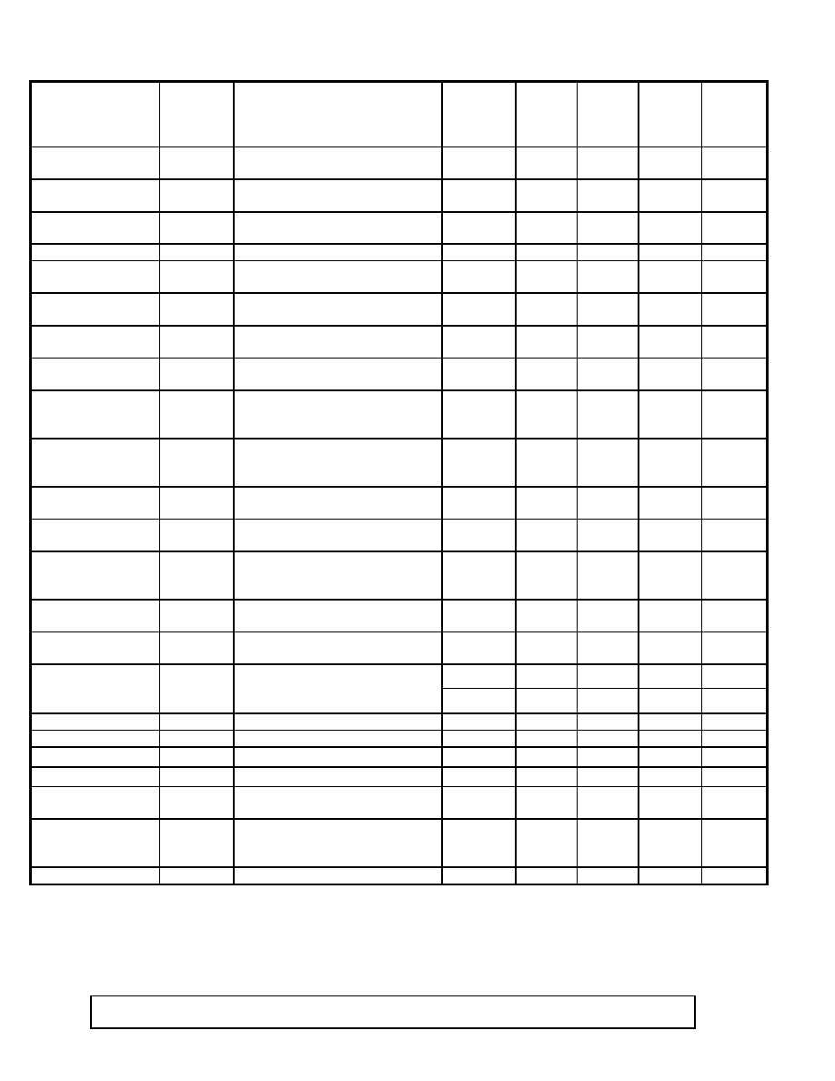
TABLE 1 ELECTRICAL TESTS
PARAMETER
Symbol
CONDITIONS
-55
∞
C <=T
A
<= +125
∞
C
V
CC
=+4.5V to +5.5V
Unless otherwise specified
Group A
Subgroup
Device
type
Limits
Min
Limits
Max
Units
DC OPERATING
CONDITIONS
Primary Power
Supply
V
CCl
NOTE 1
1,2,3
01
5.5 V
Input Voltage High
V
IH
NOTE 1
1,2,3
01
2.4
+V
CCl
+0.3
V
Input Voltage Low
V
IL
NOTE 1
1,2,3
01
-0.3
0.8 V
Battery Voltage
V
BATT
NOTE 2, 6
1,2,3
01
2.5
3.7 V
Battery Output
BAT
NOTE 1
1,2,3
01
V
BATT
-0.1
V
DC/AC ELECTRICAL
CHARACTERISTICS
Leakage Current
I
LO
1,2,3
01
-1.0
1.0
µ
A
Output Current,
__ __
PF, BF NOTE 3
I
OH
V
OH
=2.4V
1,2,3
01
-1.0
mA
Output Current,
__ __
PF, BF
I
OL
V
OL
=0.4V
1,2,3
01
4.0 mA
Input Supply
Current NOTE 4
I
CCl
1,2,3
01
3.33 mA
V
CCO
Output
Current
I
CCO
V
CCO
=V
CCl
-0.2V, Both V
CCO
pins
1,2,3
01
250 mA
Power-Fail Trip
Point NOTES 2, 5
V
TP
__
PF pin
1,2,3
01
1.26 x
V
BATT
-
250mV
1.26 x
V
BATT
+
250mV
V
V
CCO
Output
Current NOTE 7
I
CCO2
V
CCl
<V
BATT,
V
CCO
=V
BATT
-0.2V
Both V
CCO
pins
1,2,3
01
15
mA
Battery Leakage
NOTE 8
I
BATT
V
CCl
<V
BATT
1,2,3
01
10
µ
A
BAT Output Current
NOTE 9
I
BATT
OUT
V
CCl
<V
BATT
BAT pin
1
2,3
01
01
100
10
nA
µ
A
Input Capacitance
C
IN
NOTE 10
4
01
10 pF
Output Capacitance
C
OUT
NOTE 10
4
01
10 pF
V
CCl
Fall Time
t
F
VCC=4.0V to 5.5V
9,10,11
01
300
µ
s
V
CCl
Rise Time
t
R
VCC=4.0V to 5.5V
9,10,11
01
1
µ
s
__ Power Down to
PF Low
t
PF
VCC=4.0V to 5.5V
9,10,11
01
0
µ
s
__
PF High after Power
Up
t
REC
VCC=4.0V to 5.5V
9,10,11
01
100
µ
s
RST Pulse Width
RST
PW
VCC=4.0V to 5.5V
9,10,11
01
50
ns
----------------------------
Electrical Characteristics of MAX1259M/883B
19-0206
Rev. C
for /883B and SMD 5962-93264
Page 3 of
6
NOTE 1: All voltages referenced to ground.
NOTE 2: Trip-point voltage for Power-Fail Detect: V
TP
=1.26 x V
BATT
. For 5% operation: V
BATT
=3.7V max.
NOTE 3: 50pF load capacity. __ __
NOTE 4: Measured with pins BF, PF, V
CCO
and open. __
NOTE 5: __ V
TP
is the point at which PF is driven low.
NOTE 6: V
BATTF
is the point at which BF is driven low.
NOTE 7: I
CCO2
may be limited by battery capacity.
NOTE 8: Battery leakage is the internal energy consumed by the MAX1259.
NOTE 9: See Commercial Datasheet, Typical Operating Characteristics; BAT Switch Drop vs. Battery Voltage.
NOTE 10: Guaranteed by design. Not tested.
Package
ORDERING INFORMATION:
SMD
16 pin CERDIP
MAX1259MJE/883B
5962-9326401MEA
20 pin LCC
MAX1259MLP/883B
5962-9326401M2C
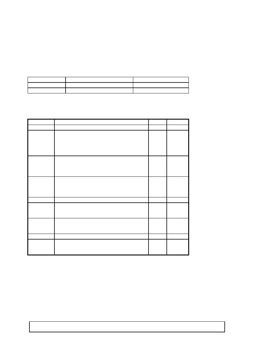
TERMINAL CONNECTIONS AND FUNCTION:
NAME
FUNCTION
J16
20LCC
V
BATT
Backup Battery Input
2
2
__
BF
__ Battery-Fail Output.
BF is high for V
CCl
at or above V
TP
and the backup
battery greater than 2V. If the backup__ battery is
below 2V or V
CCl
falls below V
TP
, BF will be
driven low.
3
4
BAT
Battery Output. During normal operation, the
BAT output supplies up to 1mA of continuous
battery current. In shipping mode, the BAT
output is high impedance.
5
7
RST
Battery-Disconnect Input. The RST input is used
to prevent battery discharge during shipping.
Pulsing the RST input disconnects the battery
from the V
CCO
and BAT outputs.
6
8
GND
Ground.
7,8
10,11
__
PF
__ Power Fail Output.
PF is high for V
CCl
greater than 1.26 x V
BATT
(V
TP
), indicating a valid V
CCl
voltage.
11
12
V
CCO
CMOS RAM is powered from V
CCO
. The battery
switchover circuit compares V
CCl
to the V
BATT
input, and connects V
CCO
to whichever is higher.
12,13
16,17
V
CCl
+5V V
CC
Input
15, 16
1, 20
NC
No connect
1,4,9,
10,14
3,5,6,9,
13,14,15,
18,19
----------------------------
Electrical Characteristics of MAX1259M/883B
19-0206
Rev. C
for /883B and SMD 5962-93264
Page 4 of
6
QUALITY ASSURANCE
Sampling and inspection procedures shall be in accordance with MIL-Prf-38535, Appendix A as specified in Mil-
Std-883.
Screening shall be in accordance with Method 5004 of Mil-Std-883. Burn-in test Method 1015:
1. Test Condition, A, B, C, or D.
2. TA = +125
∞
C minimum.
3. Interim and final electrical test requirements shall be specified in Table 2.
Quality conformance inspection shall be in accordance with Method 5005 of Mil-Std-883, including Groups A, B,
C, and D inspection.
Group A inspection:
1. Tests as specified in Table 2.
2. Selected subgroups in Table 1, Method 5005 of Mil-Std-883 shall be omitted.
Group C and D inspections:
a. End-point electrical parameters shall be specified in Table 1.
b. Steady-state life test, Method 1005 of Mil-Std-883:
1. Test condition A, B, C, D.
2. TA = +125
∞
C, minimum.
3. Test duration, 1000 hours, except as permitted by Method 1005 of Mil-Std-883.
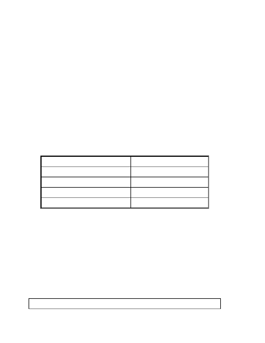
TABLE 2. ELECTRICAL TEST REQUIREMENTS
Mil-Std-883 Test Requirements
Subgroups
per Method 5005, Table 1
Interim Electric Parameters
Method 5004
1
Final Electrical Parameters
Method 5005
1*, 2, 3, 9
Group A Test Requirements
Method 5005
1, 2, 3, 9, 10, 11
Group C and D End-Point Electrical Parameters
Method 5005
1
* PDA applies to Subgroup 1 only.
----------------------------
Electrical Characteristics of MAX1259M/883B
19-0206
Rev. C
for /883B and SMD 5962-93264
Page 5 of
6