 | –≠–ª–µ–∫—Ç—Ä–æ–Ω–Ω—ã–π –∫–æ–º–ø–æ–Ω–µ–Ω—Ç: MAX1270C | –°–∫–∞—á–∞—Ç—å:  PDF PDF  ZIP ZIP |
General Description
The MAX1270/MAX1271 are multirange, 12-bit data-
acquisition systems (DAS) that require only a single +5V
supply for operation, yet accept signals at their analog
inputs that may span above the power-supply rail and
below ground. These systems provide eight analog
input channels that are independently software pro-
grammable for a variety of ranges: ±10V, ±5V, 0 to
+10V, 0 to +5V for the MAX1270; ±V
REF
, ±V
REF
/2, 0 to
V
REF
, 0 to V
REF
/2 for the MAX1271. This range switch-
ing increases the effective dynamic range to 14 bits and
provides the flexibility to interface 4≠20mA, ±12V, and
±15V powered sensors directly to a single +5V system.
In addition, these converters are fault protected to
±16.5V; a fault condition on any channel will not affect
the conversion result of the selected channel. Other fea-
tures include a 5MHz bandwidth track/hold, software-
selectable internal/external clock, 110ksps throughput
rate, and internal 4.096V or external reference opera-
tion.
The MAX1270/MAX1271 serial interface directly con-
nects to SPITM/QSPITM and MICROWIRETM devices with-
out external logic.
A hardware shutdown input (SHDN) and two software-
programmable power-down modes, standby (STBYPD)
or full power-down (FULLPD), are provided for low-cur-
rent shutdown between conversions. In standby mode,
the reference buffer remains active, eliminating start-up
delays.
The MAX1270/MAX1271 are available in 24-pin narrow
DIP or space-saving 28-pin SSOP packages.
Applications
Industrial Control Systems
Data-Acquisition Systems
Robotics
Automatic Testing
Battery-Powered Instruments
Medical Instruments
Features
o 12-Bit Resolution, 1/2LSB Linearity
o +5V Single-Supply Operation
o SPI/QSPI and MICROWIRE-Compatible
3-Wire Interface
o Four Software-Selectable Input Ranges
MAX1270: 0 to +10V, 0 to +5V, ±10V, ±5V
MAX1271: 0 to V
REF
, 0 to V
REF
/2, ±V
REF
,
±V
REF
/2
o Eight Analog Input Channels
o 110ksps Sampling Rate
o ±16.5V Overvoltage-Tolerant Input Multiplexer
o Internal 4.096V or External Reference
o Two Power-Down Modes
o Internal or External Clock
o 24-Pin Narrow DIP or 28-Pin SSOP Packages
MAX1270/MAX1271
Multirange, +5V, 8-Channel,
Serial 12-Bit ADCs
____________________________________________________________ Maxim Integrated Products
7-169
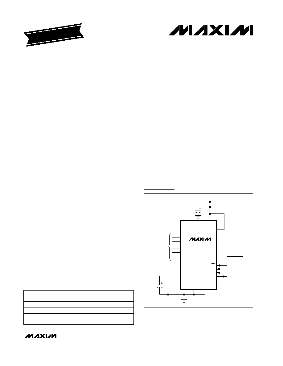
Typical Operating Circuit
19-4782; Rev 1; 3/99
PART
MAX1270ACNG
MAX1270BCNG
MAX1270ACAI
0∞C to +70∞C
0∞C to +70∞C
0∞C to +70∞C
TEMP.
RANGE
PIN-PACKAGE
24 Narrow Plastic DIP
24 Narrow Plastic DIP
28 SSOP
EVALUATION KIT MANUAL
FOLLOWS DATA SHEET
Ordering Information continued at end of data sheet.
Ordering Information
Pin Configurations appear at end of data sheet.
INL
(LSB)
±1/2
±1
±1/2
MAX1270BCAI
0∞C to +70∞C
28 SSOP
±1
V
DD
CH0
CH1
CH2
CH3
CH4
CH5
CH6
CH7
DGND
0.01
µF
4.7
µF
0.1
µF
SHDN
MAX1270
MAX1271
+5V
ANALOG
INPUTS
CS
SCLK
DIN
DOUT
SSTRB
I/O
SCK
MOSI
MISO
REF
REFADJ
AGND
MC68HCXX
SPI and QSPI are trademarks of Motorola, Inc.
MICROWIRE is a trademark of National Semiconductor Corp.
For free samples & the latest literature: http://www.maxim-ic.com, or phone 1-800-998-8800.
For small orders, phone 1-800-835-8769.
dB
MAX1270/MAX1271
Multirange, +5V, 8-Channel,
Serial 12-Bit ADCs
7-170
___________________________________________________________________________________
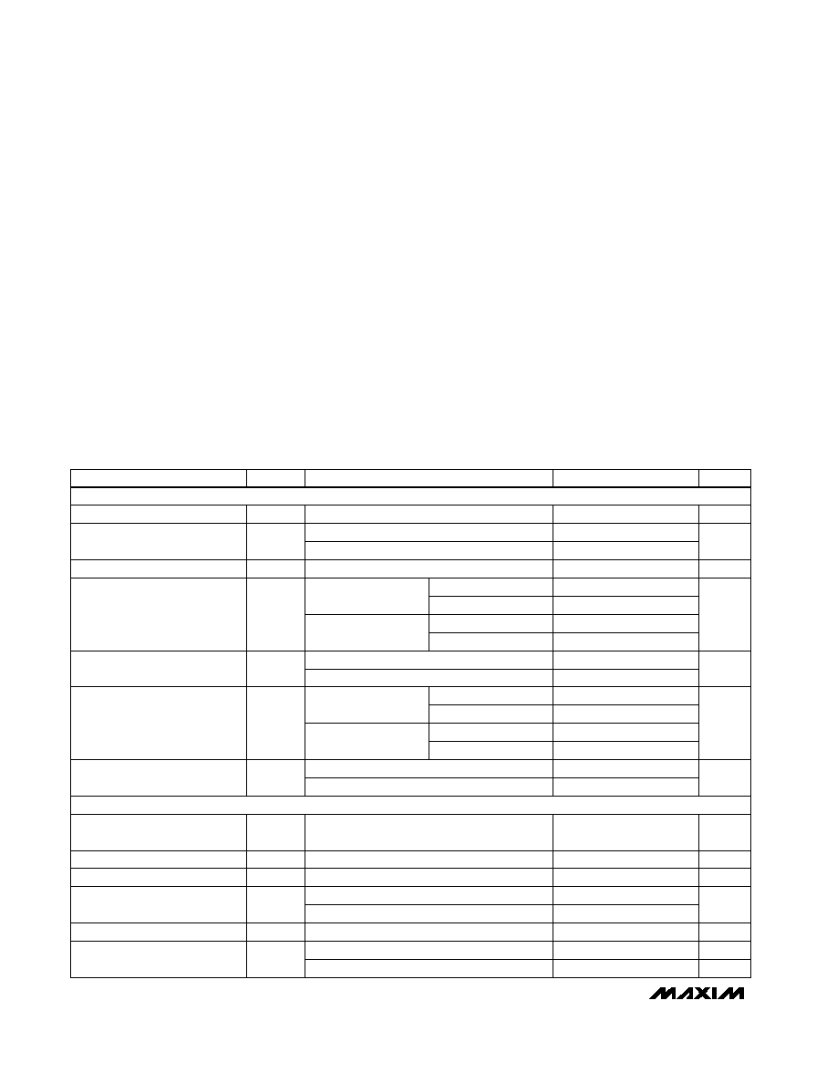
ABSOLUTE MAXIMUM RATINGS
ELECTRICAL CHARACTERISTICS
(V
DD
= +5.0V ±5%; unipolar/bipolar range; external reference mode, V
REF
= +4.096V; 4.7µF at REF; external clock, f
CLK
= 2.0MHz
(50% duty cycle), 18 clock/conversion cycle, 110ksps; T
A
= T
MIN
to T
MAX
; unless otherwise noted. Typical values are T
A
= +25∞C.)
Stresses beyond those listed under "Absolute Maximum Ratings" may cause permanent damage to the device. These are stress ratings only, and functional
operation of the device at these or any other conditions beyond those indicated in the operational sections of the specifications is not implied. Exposure to
absolute maximum rating conditions for extended periods may affect device reliability.
V
DD
to AGND............................................................-0.3V to +6V
AGND to DGND.....................................................-0.3V to +0.3V
CH0≠CH7 to AGND ......................................................... ±16.5V
REF, REFADJ to AGND ..............................-0.3V to (V
DD
+ 0.3V)
SSTRB, DOUT to DGND.............................-0.3V to (V
DD
+ 0.3V)
SHDN, CS, DIN, SCLK to DGND..............................-0.3V to +6V
Max Current into Any Pin ....................................................50mA
Continuous Power Dissipation (T
A
= +70∞C)
24-Pin Narrow DIP (derate 13.33mW/∞C above +70∞C) ..1067mW
28-Pin SSOP (derate 9.52mW/∞C above +70∞C) ..........762mW
Operating Temperature Ranges
MAX127_C_ _ ......................................................0∞C to +70∞C
MAX127_E_ _....................................................-40∞C to +85∞C
Storage Temperature Range ............................-65∞C to +150∞C
Lead Temperature (soldering, 10sec) ............................+300∞C
MAX127_B
LSB
±0.1
MAX127_A
Channel-to-Channel Offset
Error Matching
Up to the 5th harmonic
dB
-87
-78
THD
Total Harmonic Distortion
Unipolar
MAX127_A
Bipolar
MAX127_B
No missing codes over temperature
Unipolar
CONDITIONS
Bipolar
Unipolar, external reference
Bipolar, external reference
±10
LSB
±7
±0.3
Gain Error
(Note 2)
dB
70
SINAD
Signal-to-Noise + Distortion
Ratio
DYNAMIC SPECIFICATIONS
±7
±10
ppm/∞C
±3
Gain Error Temperature
Coefficient (Note 2)
±5
DC, V
IN
= ±16.5V
50kHz (Note 3)
LSB
±0.5
INL
Integral Nonlinearity
bits
12
ACCURACY (Note 1)
Resolution
External clock mode
External clock mode
±10
±5
±1.0
LSB
±1
DNL
Differential Nonlinearity
LSB
±3
Offset Error
±5
UNITS
MIN
TYP
MAX
SYMBOL
PARAMETERS
Internal clock mode
-96
dB
-86
dB
80
SFDR
Spurious-Free Dynamic Range
Channel-to-Channel Crosstalk
ns
15
Aperture Delay
ps
<50
Aperture Jitter
ns
10
MAX127_A
MAX127_B
MAX127_A
MAX127_B
Unipolar
Bipolar
MAX127_A
MAX127_B
ACCURACY (Note 1)
DYNAMIC SPECIFICATIONS (10kHz sine-wave input, ±10Vp-p (MAX1270), or ±4.096Vp-p (MAX1271), f
SAMPLE
= 110ksps)
MAX1270/MAX1271
Multirange, +5V, 8-Channel,
Serial 12-Bit ADCs
____________________________________________________________________________________
7-171
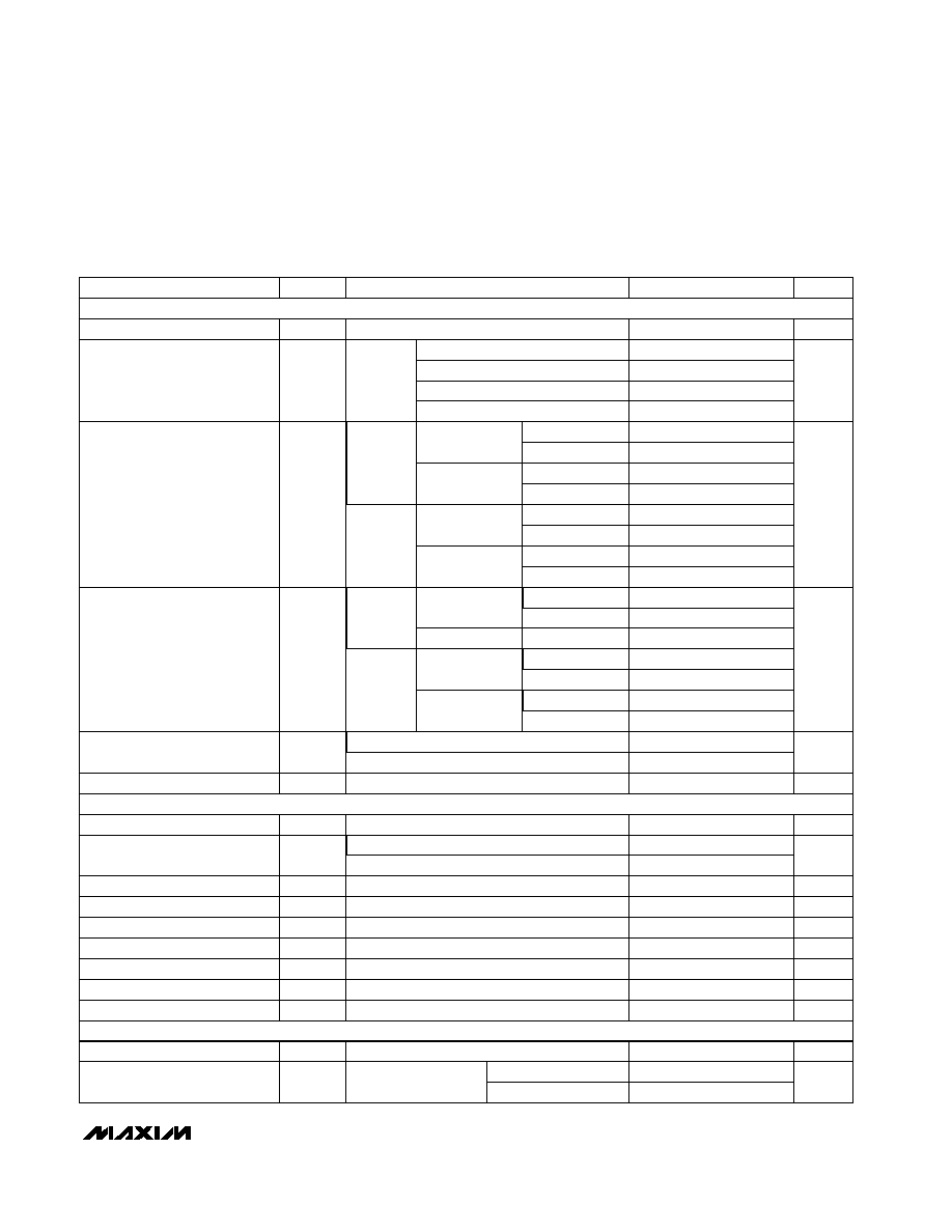
ELECTRICAL CHARACTERISTICS (continued)
(V
DD
= +5.0V ±5%; unipolar/bipolar range; external reference mode, V
REF
= +4.096V; 4.7µF at REF; external clock, f
CLK
= 2.0MHz
(50% duty cycle), 18 clock/conversion cycle, 110ksps; T
A
= T
MIN
to T
MAX
; unless otherwise noted. Typical values are T
A
= +25∞C.)
FULLPD
Normal or STBYPD
±V
REF
/2 range
MAX1271
±V
REF
range
±5V range
MAX1270
±10V range
MAX1271
0 to 5V range
MAX1270
0 to 10V range
MAX1271
RNG = 1
MAX1270
RNG = 1
MAX1271
RNG = 1
±10V or ±V
REF
range
±5V or ±V
REF
/
2
range
0 to 10V or 0 to V
REF
range
RNG = 1
MAX1270
0 to 5V or 0 to V
REF
/
2
range
1
INTERNAL REFERENCE
Input Capacitance
40
pF
16
Dynamic Resistance
V
IN
/
I
IN
21
k
REF Output Voltage
V
REF
4.076
4.096
4.116
V
REF Output Tempco
TC V
REF
±15
ppm/∞C
-600
360
-1200
10
-600
10
Buffer Voltage Gain
1.638
V/V
REFADJ Adjustment Range
±1.5
%
REFADJ Output Voltage
2.465
2.500
2.535
V
Capacitive Bypass at REFADJ
0.01
µF
REFERENCE INPUT (Reference
Input Voltage Range
2.40
4.18
V
Load Regulation (Note 5)
Output Short Circuit Current
30
mA
10
mV
Capacitive Bypass at REF
4.7
µF
Figure 1
(Note 4)
Bipolar
Unipolar
T
A
= +25∞C
MAX1270_C/MAX1271_C
0 to 0.5mA output current
Input Current
400
µA
V
REF
= 4.18V
±30
MAX1270_E/MAX1271_E
ANALOG INPUT
Track/Hold Acquisition Time
t
ACQ
3
µs
Small-Signal Bandwidth
5
MHz
Input Current
I
IN
-10
720
µA
-V
REF
V
REF
-10
10
0
V
REF
-10
360
-10
0.1
10
2.5
1.25
Input Voltage Range
V
IN
0
10
V
Unipolar
Bipolar
(BIP = 1),
Table 3
PARAMETERS
SYMBOL
MIN
TYP
MAX
UNITS
f
CLK
= 2.0MHz
-3dB
rolloff
Unipolar
(BIP = 0),
Table 3
-1200
720
Bipolar
2.5
CONDITIONS
ANALOG INPUT
INTERNAL REFERENCE
REFERENCE INPUT (Reference buffer disabled, reference input applied to REF)
RNG = 0
0
5
0
V
REF
/2
RNG = 0
RNG = 0
RNG = 0
-5
5
-V
REF
/2
V
REF
/2
MAX1270/MAX1271
Multirange, +5V, 8-Channel,
Serial 12-Bit ADCs
7-172
___________________________________________________________________________________
ELECTRICAL CHARACTERISTICS (continued)
(V
DD
= +5.0V ±5%; unipolar/bipolar range; external reference mode, V
REF
= +4.096V; 4.7µF at REF; external clock, f
CLK
= 2.0MHz
(50% duty cycle), 18 clock/conversion cycle, 110ksps; T
A
= T
MIN
to T
MAX
; unless otherwise noted. Typical values are T
A
= +25∞C.)
C
REF
= 33µF
C
REF
= 4.7µF
FULLPD
Normal or STBYPD
Reference Buffer Settling Time
8
ms
Bandgap Reference Start-Up
Time (Note 9)
200
µs
60
DIGITAL INPUTS: DIN, SCLK,
0.4
Output Voltage Low
V
OL
0.4
V
DIGITAL OUTPUTS: DOUT,
Input Capacitance
C
IN
15
pF
Output Voltage High
V
OH
V
DD
- 0.5
V
Three-State Leakage Current
I
L
-10
10
µA
Input Hysteresis
Input Low Threshold Voltage
V
IL
0.8
V
V
HYS
0.2
V
Input Leakage Current
I
IN
-10
10
µA
I
SINK
= 16mA
I
SINK
= 5mA
(Note 4)
I
SOURCE
= 0.5mA
CS = V
DD
Power-up
Three-State Output Capacitance
C
OUT
V
IN
= 0 to V
DD
15
pF
CS = V
DD
(Note 4)
Input High Threshold Voltage
V
IH
2.4
V
Supply Current
I
DD
18
Supply Voltage
V
DD
4.75
5.25
V
POWER REQUIREMENT
REFADJ Threshold for Buffer
Disable
V
DD
- 0.5
V
6
10
Input Resistance
10
k
4.18
M
Conversion Time
t
CONV
6
µs
3
5
Acquisition Phase
3
µs
External Clock Frequency
Range
f
CLK
0.1
2.0
MHz
6
7.7
11
Throughput Rate
110
ksps
Power-Supply Rejection
Ratio (Note 7)
PSRR
±0.1
±0.5
±0.5
TIMING
External clock mode (Note 8)
Internal clock mode, Figure 9
External clock mode (Note 8)
Internal clock mode, Figure 9
Normal
External clock mode
STBYPD power down mode (Note 6)
External reference = 4.096V
Internal reference
43
Internal clock mode
V
REF
= 4.18V
120
220
FULLPD power down mode
SYMBOL
MIN
TYP
MAX
UNITS
CONDITIONS
To 0.1mV, REF
bypass capacitor
fully discharged
Unipolar range
Bipolar range
POWER REQUIREMENT
DIGITAL INPUTS: DIN, SCLK, CS, SHDN
DIGITAL OUTPUTS: DOUT, SSTRB
mA
PARAMETERS
LSB
700
850
µA
TIMING
MAX1270/MAX1271
Multirange, +5V, 8-Channel,
Serial 12-Bit ADCs
____________________________________________________________________________________
7-173
TIMING CHARACTERISTICS
(V
DD
= +4.75V to +5.25; unipolar/bipolar range; external reference mode, V
REF
= +4.096V; 4.7µF at REF; external clock, f
CLK
=
2MHz; T
A
= T
MIN
to T
MAX
, unless otherwise noted. Typical values are T
A
= +25∞C.) (Figures 2, 5, 7, 10)
DIN to SCLK Setup
t
DS
100
DIN to SCLK Hold
t
DH
0
SCLK Fall to Output Data Valid
t
DO
C
LOAD
= 100pF
20
170
CS Fall to Output Enable
t
DV
C
LOAD
= 100pF
120
CS Rise to Output Disable
t
TR
C
LOAD
= 100pF
100
CS to SCLK Rise Setup
t
CSS
100
CS to SCLK Rise Hold
t
CSH
0
SCLK Pulse Width High
t
CH
200
SCLK Pulse Width Low
t
CL
200
SCLK Fall to SSTRB
t
SSTRB
C
LOAD
= 100pF
200
CS to SSTRB Output Enable
t
SDV
C
LOAD
= 100pF
External clock mode only
200
CS to SSTRB Output Disable
t
STR
C
LOAD
= 100pF
External clock mode only
200
ns
ns
ns
ns
ns
ns
ns
ns
ns
ns
ns
ns
SSTRB Rise to SCLK Rise
(Note 4)
t
SCK
Internal clock mode only
0
ns
PARAMETERS
SYMBOL
CONDITIONS
MIN
TYP
MAX
UNITS
Note 1: Accuracy specifications tested at V
DD
= +5.0V. Performance at power-supply tolerance limit is guaranteed by Power-Supply
Rejection test.
Note 2: External reference: V
REF
= 4.096V, offset error nulled. Ideal last-code transition = FS - 3/2LSB.
Note 3: Ground "on" channel; sine wave applied to all "off" channels. V
IN
= ±5V (MAX1270), V
IN
= ±4V (MAX1271).
Note 4: Guaranteed by design, not production tested.
Note 5: Use static external loads during conversion for specified accuracy.
Note 6: Tested using internal reference.
Note 7: PSRR measured at full scale. Tested for the ±10V (MAX1270) and ±4.096V (MAX1271) input ranges.
Note 8: Acquisition phase and conversion time are dependent on the clock period; clock has 50% duty cycle (Figure 6).
Note 9: Not production tested. Provided for design guidance only.