General Description
The MAX1272/MAX1273 multirange 12-bit data-acquisi-
tion systems (DAS) operate with a single 5V supply. The
software-programmable analog input accepts a variety
of voltage ranges: ±10V, ±5V, 0 to 10V, 0 to 5V for the
MAX1272; ±V
REF
, ±V
REF
/ 2, 0 to V
REF
, 0 to V
REF
/ 2 for
the MAX1273. The software-selectable extended analog
input range increases the effective dynamic range to 14
bits and provides the flexibility to interface 4≠20mA pow-
ered sensors directly to a single 5V system. In addition,
the MAX1272 provides fault protection to ±12V. Other
features include a 5MHz track/hold (T/H) bandwidth,
87ksps throughput rate, and internal (4.096V) or external
(2.40V to 4.18V) reference.
The MAX1272/MAX1273 serial interfaces connect
directly to SPITM/QSPITM/MICROWIRETM-compatible
devices without any external logic.
Four software-programmable power-down modes
(delayed standby, immediate standby, delayed full power-
down, and immediate full power-down) provide low-cur-
rent shutdown between conversions. In standby mode, the
internal reference buffer remains active, thus eliminating
startup delay.
The MAX1272/MAX1273 are available in 8-pin PDIP
and µMAX packages. Both devices are available in the
commercial (0∞C to +70∞C) or extended (-40∞C to
+85∞C) temperature range.
Applications
Industrial Control Systems
Data-Acquisition Systems
Robotics
Automatic Testing
Battery-Powered Instruments
Medical Instruments
Features
o Four Software-Selectable Input Ranges
MAX1272: 0 to 10V, 0 to 5V, ±10V, ±5V
MAX1273: 0 to V
REF
, 0 to V
REF
/ 2, ±V
REF
,
±V
REF
/ 2
o 12-Bit Resolution, No Missing Codes
o 5V Single-Supply Operation
o SPI/QSPI/MICROWIRE-Compatible 3-Wire
Interface
o 87ksps Sampling Rate
o ±12V Fault-Protected Analog Input (MAX1272)
o Internal (4.096V) or External (2.4V to 4.18V)
Reference
o Low Power
1.5mA at 87ksps
0.4mA at 10ksps
0.2mA at 1ksps
o Four Power-Down Modes
o 8-Pin µMAX and PDIP Packages
MAX1272/MAX1273
Fault-Protected, 12-Bit ADCs
with Software-Selectable Input Range
________________________________________________________________ Maxim Integrated Products
1
REF
AIN
GND
1
2
8
7
DOUT
CS
DIN
V
DD
SCLK
PDIP/
µMAX
TOP VIEW
3
4
6
5
MAX1272
MAX1273
Pin Configuration
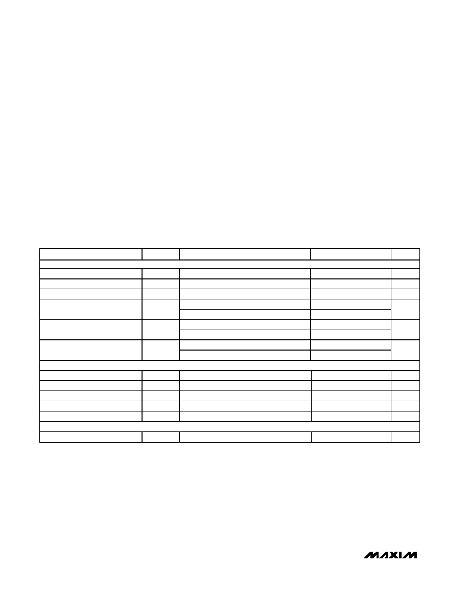
Ordering Information
19-2921; Rev 1; 12/03
For pricing, delivery, and ordering information, please contact Maxim/Dallas Direct! at
1-888-629-4642, or visit Maxim's website at www.maxim-ic.com.
PART
TEMP
RANGE
PIN-
PACKAGE
INL
(LSB)
MAX1272CPA
0
∞C to +70∞C
8 Plastic DIP
±
1
MAX1272CUA
0
∞C to +70∞C
8 µMAX
±
1
MAX1272EPA
-40
∞C to +85∞C
8 Plastic DIP
±
1
MAX1272EUA
-40
∞C to +85∞C
8 µMAX
±
1
MAX1273CPA
0
∞C to +70∞C
8 Plastic DIP
±
1
MAX1273CUA
0
∞C to +70∞C
8 µMAX
±
1
MAX1273EPA
-40
∞C to +85∞C
8 Plastic DIP
±
1
MAX1273EUA
-40
∞C to +85∞C
8 µMAX
±
1
SPI and QSPI are trademarks of Motorola, Inc.
MICROWIRE is a trademark of National Semiconductor Corp.
Typical Application Circuit appears at end of data sheet.
MAX1272/MAX1273
Fault-Protected, 12-Bit ADCs
with Software-Selectable Input Range
2
_______________________________________________________________________________________
ABSOLUTE MAXIMUM RATINGS
Stresses beyond those listed under "Absolute Maximum Ratings" may cause permanent damage to the device. These are stress ratings only, and functional
operation of the device at these or any other conditions beyond those indicated in the operational sections of the specifications is not implied. Exposure to
absolute maximum rating conditions for extended periods may affect device reliability.
V
DD
to GND ..............................................................-0.3V to +6V
AIN to GND (MAX1272) ...................................................... ±12V
AIN to GND (MAX1273) ........................................................ ±6V
DOUT, CS, DIN, SCLK, REF to GND..........-0.3V to (V
DD
+ 0.3V)
Maximum Current into Any Pin............................................50mA
Continuous Power Dissipation (T
A
= +70∞C)
8-Pin Plastic DIP (derate 9.1mW/∞C above +70∞C) ......727mW
8-Pin µMAX (derate 4.5mW/∞C above +70∞C) ..............362mW
Operating Temperature Ranges
MAX127_ C_ _ .....................................................0∞C to +70∞C
MAX127_ E_ _...................................................-40∞C to +85∞C
Storage Temperature Range .............................-65∞C to +150∞C
Lead Temperature (soldering, 10s) ................................+300∞C
Junction Temperature .....................................................+150∞C
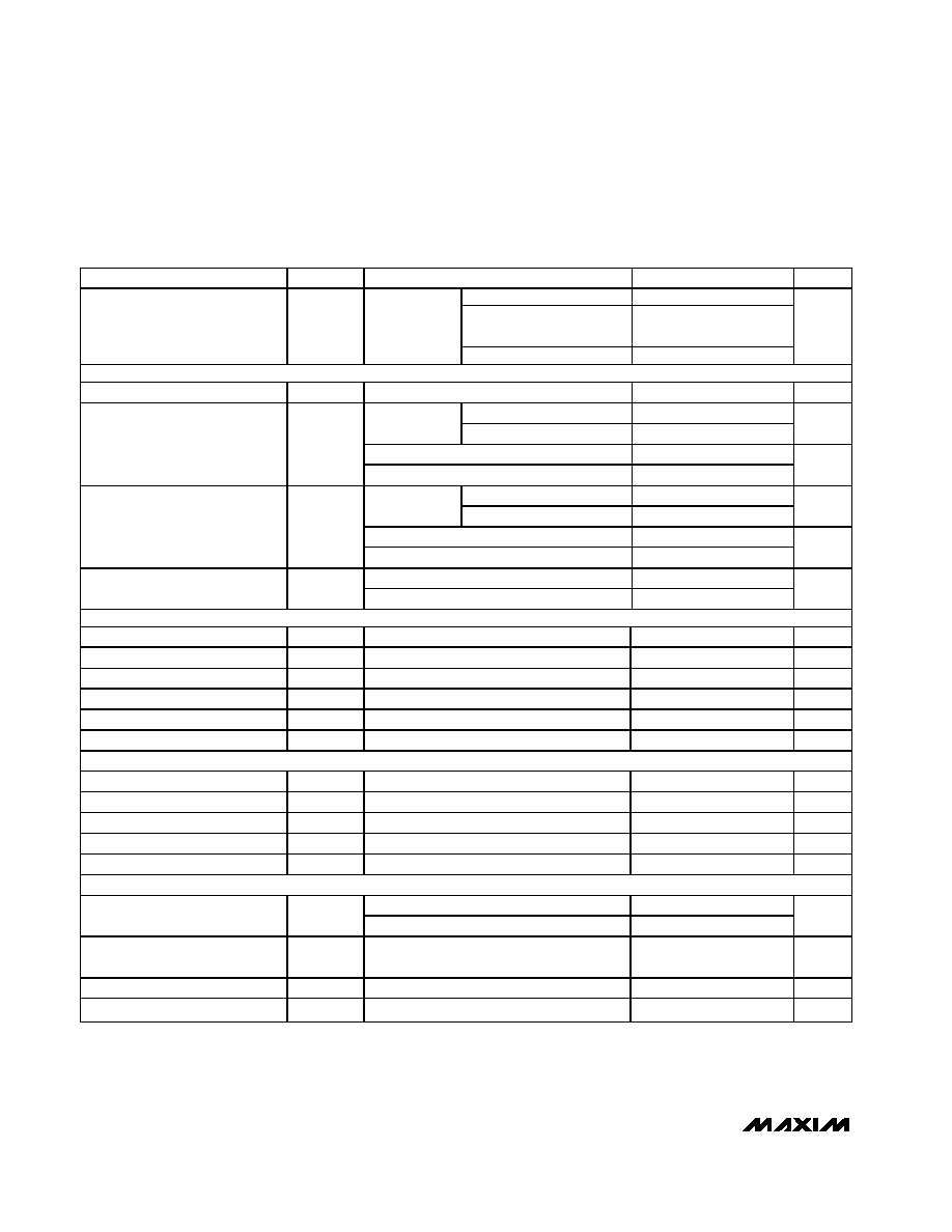
ELECTRICAL CHARACTERISTICS
(V
DD
= 4.75V to 5.25V, unipolar/bipolar input range, external reference mode, V
REF
= 4.096V, C
REF
= 1.0µF, f
SCLK
= 1.4MHz,
50% duty cycle, C
LOAD
= 50pF, T
A
= T
MIN
to T
MAX
, unless otherwise noted. Typical values are at T
A
= +25∞C.)
PARAMETERS
SYMBOL
CONDITIONS
MIN
TYP
MAX
UNITS
ACCURACY (Note 1)
Resolution
12
Bits
Integral Nonlinearity
INL
±0.3
±
1.0
LSB
Differential Nonlinearity
DNL
No missing codes over temperature
±0.35
±
1.00
LSB
Unipolar
±
5
Offset Error
Bipolar
±
10
LSB
Unipolar
±
10
Gain Error (Note 2)
Bipolar
±
10
LSB
Unipolar
±
3
Gain Error Temperature
Coefficient (Note 2)
Bipolar
±
5
ppm/∞C
DYNAMIC SPECIFICATIONS (10kHz sine-wave input, ±10V
P-P
(MAX1272), or ±4.096V
P-P
(MAX1273), f
SAMPLE
= 87ksps)
Signal-to-Noise + Distortion Ratio
SINAD
69
72
dB
Total Harmonic Distortion
THD
Up to the 5th harmonic
-87
-78
dB
Spurious-Free Dynamic Range
SFDR
80
88
dB
Aperture Delay
t
AD
15
ns
Aperture Jitter
t
AJ
<50
ps
ANALOG INPUT
T/H Acquisition Time
t
ACQ
2.85
µs

MAX1272/MAX1273
Fault-Protected, 12-Bit ADCs
with Software-Selectable Input Range
_______________________________________________________________________________________
3
ELECTRICAL CHARACTERISTICS (continued)
(V
DD
= 4.75V to 5.25V, unipolar/bipolar input range, external reference mode, V
REF
= 4.096V, C
REF
= 1.0µF, f
SCLK
= 1.4MHz,
50% duty cycle, C
LOAD
= 50pF, T
A
= T
MIN
to T
MAX
, unless otherwise noted. Typical values are at T
A
= +25∞C.)
PARAMETERS
SYMBOL
CONDITIONS
MIN
TYP
MAX
UNITS
±10V (MAX1272) or ±V
REF
(MAX1273)
range
5
±5V (MAX1272) or ±V
REF
/ 2 (MAX1273)
range
2.5
0 to 10V (MAX1272) or 0 to V
REF
(MAX1273)
range
2.5
Small-Signal Bandwidth
BW
-3dB
0 to 5V (MAX1272) or 0 to V
REF
/ 2
(MAX1273) range
1.25
MHz
RNG = 1
0
10
MAX1272
RNG = 0
0
5
RNG = 1
0
V
REF
Unipolar
MAX1273
RNG = 0
0
V
REF
/ 2
RNG = 1
-10
+10
MAX1272
RNG = 0
-5
+5
RNG = 1
-V
REF
+V
REF
Input Voltage Range
(Tables 2, 3)
V
IN
Bipolar
MAX1273
RNG = 0
-V
REF
/ 2
+V
REF
/ 2
V
0 to 10V range
-10
+860
MAX1272
0 to 5V range
-10
+430
0 to V
REF
range
-10
+10
Unipolar
MAX1273
0 to V
REF
/ 2 range
-10
+10
±10V range
-1400
+860
MAX1272
±5V range
-720
+430
±V
REF
range
-1400
+10
Input Current
I
IN
Bipolar
MAX1273
±V
REF
/ 2 range
-720
+10
µA
Input Capacitance
40
pF
INTERNAL REFERENCE
REF Output Voltage
V
REF
4.036
4.096
4.156
V
MAX127_ C
±15
REF Output Tempco
TC V
REF
MAX127_ E
±30
ppm/∞C
Output Short-Circuit Current
REF shorted to GND
40
mA
Load Regulation
0 to 0.5mA output current
0.7
10
mV
Capacitive Bypass at REF
1
µF
REFERENCE INPUT (Reference buffer disabled, reference input applied to REF)
Input Voltage Range
2.40
4.18
V
MAX1272/MAX1273
Fault-Protected, 12-Bit ADCs
with Software-Selectable Input Range
4
_______________________________________________________________________________________
ELECTRICAL CHARACTERISTICS (continued)
(V
DD
= 4.75V to 5.25V, unipolar/bipolar input range, external reference mode, V
REF
= 4.096V, C
REF
= 1.0µF, f
SCLK
= 1.4MHz,
50% duty cycle, C
LOAD
= 50pF, T
A
= T
MIN
to T
MAX
, unless otherwise noted. Typical values are at T
A
= +25∞C.)
PARAMETERS
SYMBOL
CONDITIONS
MIN
TYP
MAX
UNITS
Converting
400
850
Standby power-down
mode
5
10
Input Current
V
REF
= 4.096V
Full power-down mode
1
µA
POWER REQUIREMENTS
Supply Voltage
V
DD
4.75
5
5.25
V
Bipolar
2.4
4
Converting
Unipolar
2.2
3
mA
Standby power-down mode
400
700
Supply Current
(Internal Reference Mode)
I
DD
Full power-down mode
1
µA
Bipolar
1.5
2.5
Converting
Unipolar
1.2
2.0
mA
Standby power-down mode
200
450
Supply Current
(External Reference Mode)
I
DD
Full power-down mode
1
µA
External reference = 4.096V
±0.3
±
1.0
Power-Supply Rejection
Ratio (Note 3)
PSRR
Internal reference
±
0.5
LSB
TIMING
Clock Frequency Range
f
SCLK
0.1
1.4
MHz
T/H Acquisition Time
t
ACQ
(Note 4)
2.85
µs
Conversion Time
t
CONV
(Note 4)
8.57
µs
Throughput Rate
87.5
ksps
Internal Reference Settling Time
REF bypass capacitor initially discharged
2
ms
Device Power-Up Time
External reference mode
10
µs
DIGITAL INPUTS (DIN, SCLK, and
CS)
Input High-Threshold Voltage
V
IH
2.4
V
Input Low-Threshold Voltage
V
IL
0.8
V
Input Hysteresis
V
HYS
0.2
V
Input Leakage Current
I
IN
V
IN
= 0 to V
DD
-10
+10
µA
Input Capacitance
C
IN
15
pF
DIGITAL OUTPUT (DOUT)
I
SINK
= 10mA
0.4
Output Voltage Low
V
OL
I
SINK
= 16mA
0.6
V
Output Voltage High
V
OH
I
SOURCE
= 0.5mA
V
DD
- 0.5
V
Three-State Leakage Current
I
L
CS = V
DD
-10
+10
µA
Three-State Output Capacitance
C
OUT
CS = V
DD
15
pF
MAX1272/MAX1273
Fault-Protected, 12-Bit ADCs
with Software-Selectable Input Range
_______________________________________________________________________________________
5
TIMING CHARACTERISTICS
(V
DD
= 4.75V to 5.25V, unipolar/bipolar input range, external reference mode, V
REF
= 4.096V, C
REF
= 1.0µF, f
SCLK
= 1.4MHz,
50% duty cycle, C
LOAD
= 50pF, T
A
= T
MIN
to T
MAX
, unless otherwise noted. Typical values are at T
A
= +25∞C.) (Figures 1 and 4)
PARAMETERS
SYMBOL
CONDITIONS
MIN
TYP
MAX
UNITS
DIN to SCLK Setup
t
DS
100
ns
DIN to SCLK Hold
t
DH
0
ns
SCLK Fall to Output Data Valid
t
DO
20
250
ns
CS Fall to Output Enable
t
DV
100
ns
CS Rise to Output Disable
t
TR
100
ns
CS to SCLK Rise Setup
t
CSS
100
ns
CS to SCLK Rise Hold
t
CSH
0
ns
SCLK Pulse Width High
t
CH
200
ns
SCLK Pulse Width Low
t
CL
200
ns
Note 1: Accuracy specifications tested at V
DD
= 5V. Performance at power-supply tolerance limit is guaranteed by power-supply
rejection test.
Note 2: Offset error nulled. The ideal last-code transition is (FS - 1.5 LSB).
Note 3: PSRR measured at full scale. Tested at ±10V (MAX1272) and ±4.096V (MAX1273) input ranges.
Note 4: Acquisition and conversion times are dependent on the clock speed.
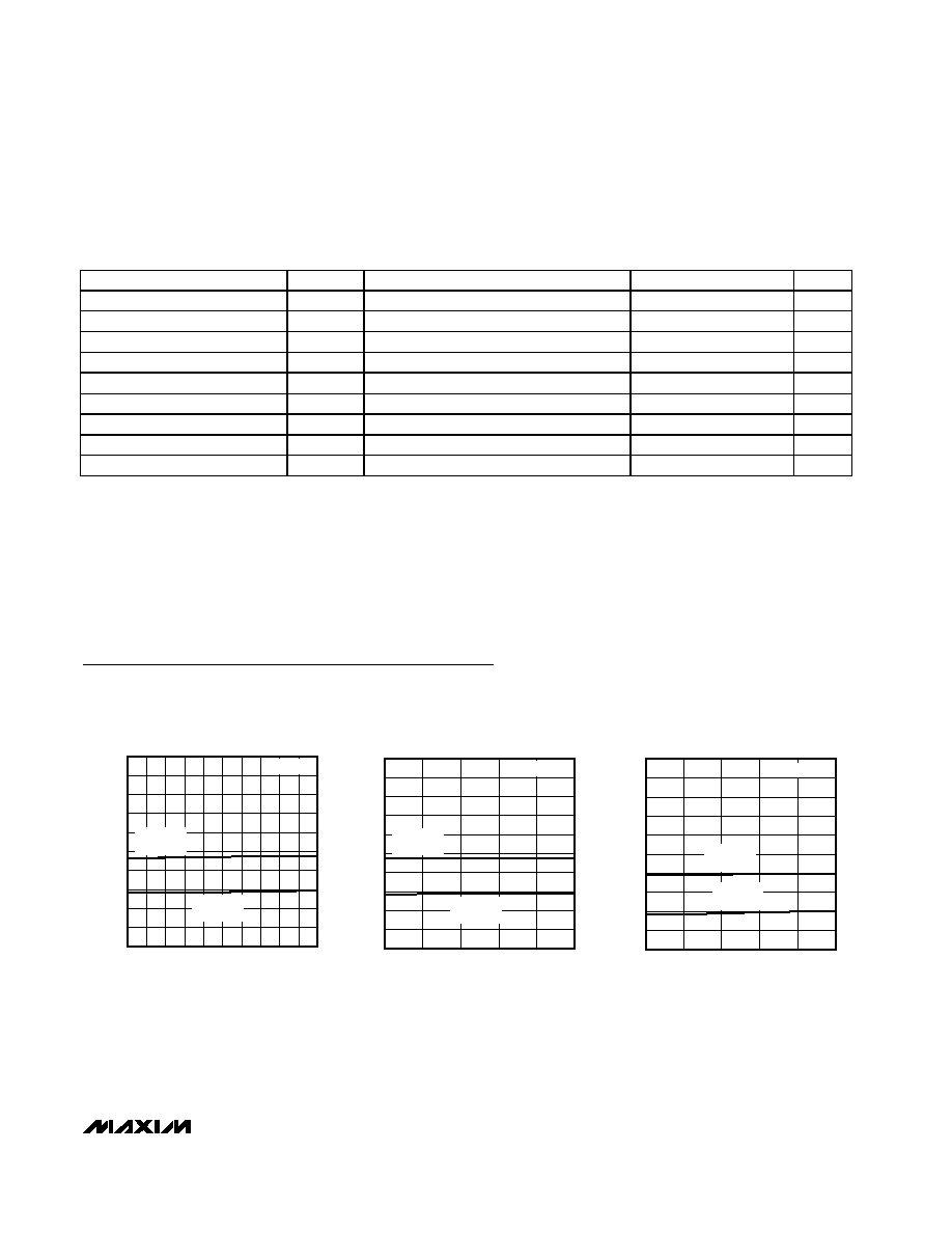
Typical Operating Characteristics
(Typical operating circuit, BIP = RNG = 1, V
DD
= 5V, external reference mode, V
REF
= 4.096V, C
REF
= 1.0µF, f
SCLK
= 1.4MHz,
50% duty cycle, 87ksps, T
A
= +25∞C, unless otherwise noted.)
CONVERTING SUPPLY CURRENT
vs. SUPPLY VOLTAGE
MAX1272/73 toc01
SUPPLY VOLTAGE (V)
SUPPLY CURRENT (mA)
5.20
5.15
5.05 5.10
4.85 4.90 4.95 5.00
4.80
0.5
1.0
1.5
2.0
2.5
3.0
3.5
4.0
4.5
5.0
0
4.75
5.25
INTERNAL
REFERENCE
EXTERNAL
REFERENCE
V
AIN
= 0
CONVERTING SUPPLY CURRENT
vs. TEMPERATURE
MAX1272/73 toc02
TEMPERATURE (
∞C)
SUPPLY CURRENT (mA)
60
35
-15
10
0.5
1.0
1.5
2.0
2.5
3.0
3.5
4.0
4.5
5.0
0
-40
85
V
AIN
= 0
INTERNAL
REFERENCE
EXTERNAL
REFERENCE
STANDBY SUPPLY CURRENT
vs. TEMPERATURE
MAX1272/73 toc03
TEMPERATURE (
∞C)
STANDBY SUPPLY CURRENT (mA)
60
35
10
-15
0.1
0.2
0.3
0.4
0.5
0.6
0.7
0.8
0.9
1.0
0
-40
85
V
AIN
= 0
INTERNAL
REFERENCE
EXTERNAL
REFERENCE