For pricing, delivery, and ordering information, please contact Maxim/Dallas Direct! at
1-888-629-4642, or visit Maxim's website at www.maxim-ic.com.
General Description
The MAX1284/MAX1285 12-bit analog-to-digital con-
verters (ADCs) combine a high-bandwidth track/hold
(T/H), a serial interface with high conversion speed, an
internal +2.5V reference, and low power consumption.
The MAX1284 operates from a single +4.5V to +5.5V
supply. The MAX1285 operates from a single +2.7V to
+3.6V supply.
The 3-wire serial interface connects directly to
SPITM/QSPITM/ MICROWIRETM devices without external
logic. The devices use an external serial-interface clock
to perform successive-approximation analog-to-digital
conversions.
Low power, ease of use, and small package size make
these converters ideal for remote-sensor and data-acqui-
sition applications or for other circuits with demanding
power consumption and space requirements. The
MAX1284/MAX1285 are available in 8-pin SO packages.
These devices are pin-compatible, higher-speed ver-
sions of the MAX1240/MAX1241. Refer to the respec-
tive data sheets for more information.
Applications
Portable Data Logging
Data Acquisition
Medical Instruments
Battery-Powered Instruments
Pen Digitizers
Process Control
____________________________Features
o Single-Supply Operation
+4.5V to +5.5V (MAX1284)
+2.7V to +3.6V (MAX1285)
o �1LSB (max) DNL, �1LSB (max) INL
o 400ksps Sampling Rate (MAX1284)
o Internal Track/Hold
o +2.5V Internal Reference
o Low Power: 2.5mA (400ksps)
o SPI/QSPI/MICROWIRE 3-Wire Serial-Interface
o Pin-Compatible, High-Speed Upgrades to
MAX1240/MAX1241
o 8-Pin SO Package
400ksps/300ksps, Single-Supply, Low-Power,
Serial 12-Bit ADCs with Internal Reference
________________________________________________________________ Maxim Integrated Products
1
19-1687; Rev 1; 7/00
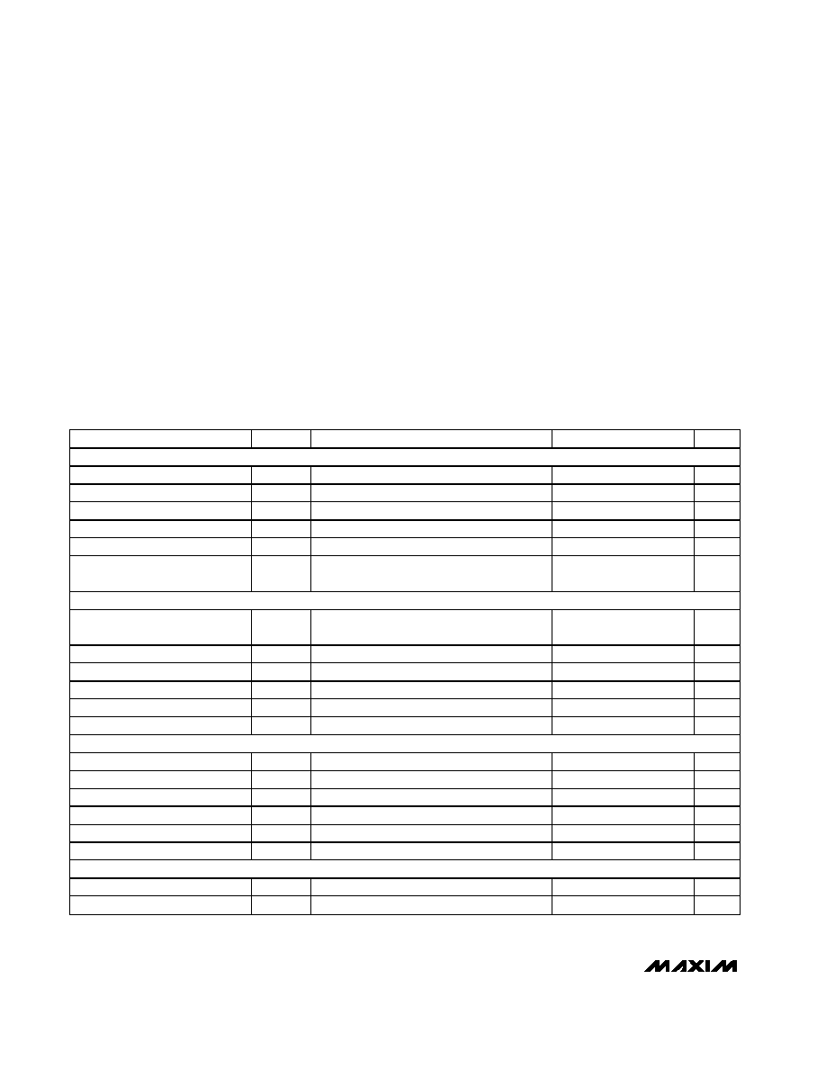
TOP VIEW
1
2
3
4
8
7
6
5
SCLK
CS
DOUT
GND
REF
SHDN
AIN
V
DD
SO
MAX1284
MAX1285
Pin Configuration
Ordering Information
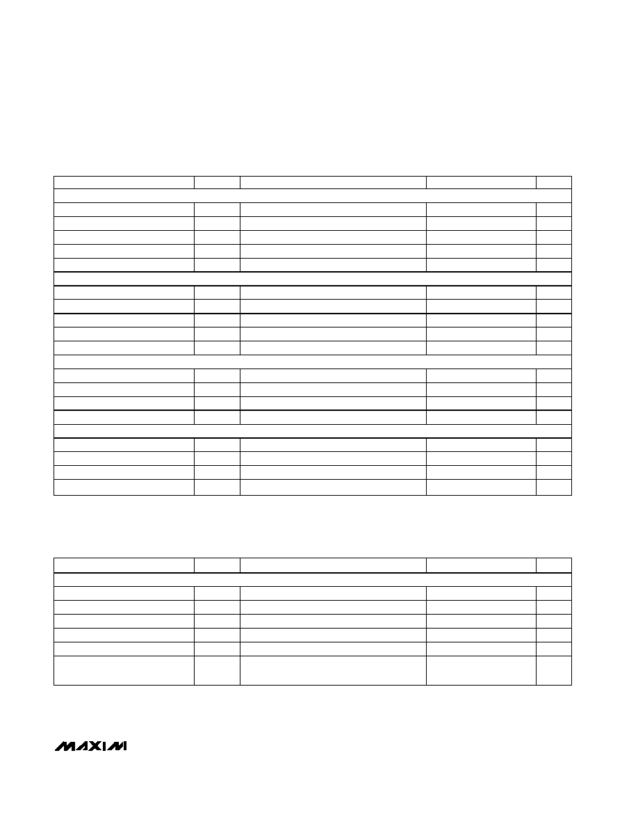
Functional Diagram
7
AIN
T/H
DOUT
6
1
OUTPUT
SHIFT
REGISTER
CONTROL
LOGIC
INT
CLOCK
12-BIT
SAR
8
2
3
5
REF
4
SHDN
+2.5V REFERENCE
GND
SCLK
CS
MAX1284
MAX1285
V
DD
SPI and QSPI are trademarks of Motorola, Inc.
MICROWIRE is a trademark of National Semiconductor Corp.
MAX1284/MAX1285
*Future product--contact factory for availability.
PART
TEMP.
RANGE
PIN-
PACKAGE
SUPPLY
VOLTAGE (V)
MAX1284BCSA
0�C to +70�C
8 SO
5
MAX1284BESA* -40�C to +85�C 8 SO
5
MAX1285BCSA
0�C to +70�C
8 SO
2.7 to 3.6
MAX1285BESA
-40�C to +85�C 8 SO
2.7 to 3.6
MAX1284/MAX1285
400ksps/300ksps, Single-Supply, Low-Power,
Serial 12-Bit ADCs with Internal Reference
2
_______________________________________________________________________________________
ELECTRICAL CHARACTERISTICS--MAX1284
(V
DD
= +4.5V to +5.5V; f
SCLK
= 6.4MHz, 50% duty cycle, 16 clocks/conversion cycle (400ksps), 4.7�F capacitor at REF, T
A
= T
MIN
to
T
MAX,
unless otherwise noted. Typical values are at T
A
= +25�C.)
V
DD
to GND .............................................................-0.3V to +6V
AIN to GND................................................-0.3V to (V
DD
+ 0.3V)
REF to GND ...............................................-0.3V to (V
DD
+ 0.3V)
Digital Inputs to GND...............................................-0.3V to +6V
DOUT to GND............................................-0.3V to (V
DD
+ 0.3V)
DOUT Current ..................................................................�25mA
Continuous Power Dissipation (T
A
= +70�C)
8-Pin SO (derate 5.88mW/�C above +70�C) ..............471mW
Operating Temperature Ranges
MAX1284BCSA/MAX1285BCSA .......................0�C to +70�C
MAX1284BESA/MAX1285BESA .....................-40�C to +85�C
Storage Temperature Range............................-60�C to +150�C
Lead Temperature (soldering, 10s) ................................+300�C
ABSOLUTE MAXIMUM RATINGS
Stresses beyond those listed under "Absolute Maximum Ratings" may cause permanent damage to the device. These are stress ratings only, and functional
operation of the device at these or any other conditions beyond those indicated in the operational sections of the specifications is not implied. Exposure to
absolute maximum rating conditions for extended periods may affect device reliability.
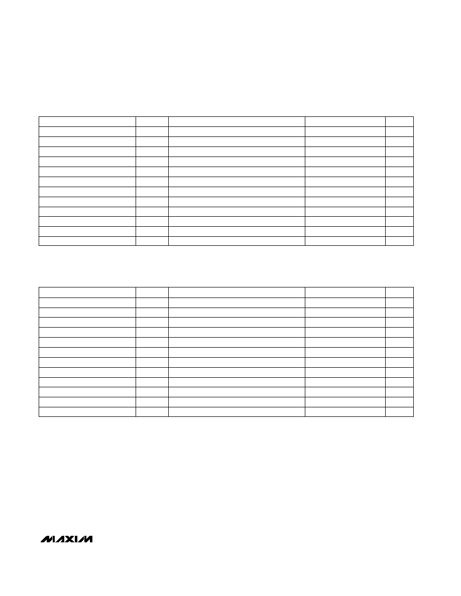
PARAMETER
SYMBOL
CONDITIONS
MIN
TYP
MAX
UNITS
DC ACCURACY (Note 1)
Resolution
12
Bits
Relative Accuracy (Note 2)
INL
�1.0
LSB
Differential Nonlinearity
DNL
No missing codes over temperature
�1.0
LSB
Offset Error
�6.0
LSB
Gain Error (Note 3)
�6.0
LSB
Gain Error Temperature
Coefficient
�0.8
ppm/�C
DYNAMIC SPECIFICATIONS (100kHz sine wave, 2.5Vp-p, clock = 6.4MHz)
Signal-to-Noise Plus Distortion
Ratio
SINAD
70
dB
Total Harmonic Distortion
THD
Up to the 5th harmonic
-80
dB
Spurious-Free Dynamic Range
SFDR
80
dB
Intermodulation Distortion
IMD
f
IN1
= 99Hz, f
IN2
= 102Hz
76
dB
Full-Power Bandwidth
-3dB point
6
MHz
Full-Linear Bandwidth
SINAD > 68dB
350
kHz
CONVERSION RATE
Conversion Time (Note 4)
t
CONV
2.5
�s
Track/Hold Acquisition Time
t
ACQ
468
ns
Aperture Delay
10
ns
Aperture Jitter
<50
ps
Serial Clock Frequency
t
SCLK
0.5
6.4
MHz
Duty Cycle
40
60
%
ANALOG INPUT (AIN)
Input Voltage Range
V
AIN
0
2.5
V
Input Capacitance
18
pF
MAX1284/MAX1285
400ksps/300ksps, Single-Supply, Low-Power,
Serial 12-Bit ADCs with Internal Reference
________________________________________________________________________________________
3
ELECTRICAL CHARACTERISTICS--MAX1284 (continued)
(V
DD
= +4.5V to +5.5V; f
SCLK
= 6.4MHz, 50% duty cycle, 16 clocks/conversion cycle (400ksps), 4.7�F capacitor at REF, T
A
= T
MIN
to
T
MAX,
unless otherwise noted. Typical values are at T
A
= +25�C.)
ELECTRICAL CHARACTERISTICS--MAX1285
(V
DD
= +2.7V to +3.6V; f
SCLK
= 4.8MHz, 50% duty cycle, 16 clocks/conversion cycle (300ksps), 4.7�F capacitor at REF, T
A
= T
MIN
to
T
MAX
, unless otherwise noted. Typical values are at T
A
= +25�C.)
PARAMETER
SYMBOL
CONDITIONS
MIN
TYP
MAX
UNITS
INTERNAL REFERENCE
REF Output Voltage
V
REF
2.48
2.50
2.52
V
REF Short-Circuit Current
T
A
= +25�C
30
mA
REF Output Tempco
TC V
REF
�15
ppm/�C
Load Regulation (Note 5)
0 to 1mA output load
0.1
2.0
mV/mA
Capacitive Bypass at REF
4.7
10
�F
DIGITAL INPUTS (SCLK, CS, SHDN)
Input High Voltage
V
INH
3.0
V
Input Low Voltage
V
INL
0.8
V
Input Hysteresis
V
HYST
0.2
V
Input Leakage
I
IN
V
IN
= 0 or V
DD
�1
�A
Input Capacitance
C
IN
15
pF
DIGITAL OUTPUT (DOUT)
Output Voltage Low
V
OL
I
SINK
= 5mA
0.4
V
Output Voltage High
V
OH
I
SOURCE
= 1mA
4
V
Three-State Leakage Current
I
L
CS = +5V
�10
�A
Three-State Output Capacitance
C
OUT
CS = +5V
15
pF
POWER SUPPLY
Positive Supply Voltage (Note 6)
VDD
4.5
5.5
V
Positive Supply Current (Note 7)
IDD
V
DD
= +5.5V
2.5
4.0
mA
Shutdown Supply Current
I
SHDN
SCLK = V
DD
, SHDN = GND
2
10
�A
Power-Supply Rejection
PSR
V
DD
= +5V �10%, midscale input
�0.5
�2.0
mV
PARAMETER
SYMBOL
CONDITIONS
MIN
TYP
MAX
UNITS
DC ACCURACY (Note 1)
Resolution
12
Bits
Relative Accuracy (Note 2)
INL
�1.0
LSB
Differential Nonlinearity
DNL
No missing codes over temperature
�1.0
LSB
Offset Error
�6.0
LSB
Gain Error (Note 3)
�6.0
LSB
Gain Error Temperature
Coefficient
�1.6
ppm/�C
MAX1284/MAX1285
400ksps/300ksps, Single-Supply, Low-Power,
Serial 12-Bit ADCs with Internal Reference
4
_______________________________________________________________________________________
ELECTRICAL CHARACTERISTICS--MAX1285 (continued)
(V
DD
= +2.7V to +3.0V; f
SCLK
= 4.8MHz, 50% duty cycle, 16 clocks/conversion cycle (300ksps), 4.7�F capacitor at REF, T
A
= T
MIN
to
T
MAX,
unless otherwise noted. Typical values are at T
A
= +25�C.)
PARAMETER
SYMBOL
CONDITIONS
MIN
TYP
MAX
UNITS
DYNAMIC SPECIFICATIONS (75kHz sine wave, 2.5Vp-p, f
SAMPLE
= 300ksps, f
SCLK
= 4.8MHz)
Signal-to-Noise Plus Distortion
Ratio
SINAD
70
dB
Total Harmonic Distortion
THD
Up to the 5th harmonic
-80
dB
Spurious-Free Dynamic Range
SFDR
80
dB
Intermodulation Distortion
IMD
f
IN1
= 73kHz, f
IN2
= 77kHz
76
dB
Full-Power Bandwidth
-3dB point
3
MHz
Full-Linear Bandwidth
SINAD > 68dB
250
kHz
CONVERSION RATE
Conversion Time (Note 4)
t
CONV
3.3
�s
Track/Hold Acquisition Time
t
ACQ
625
ns
Aperture Delay
10
ns
Aperture Jitter
<50
ps
Serial Clock Frequency
t
SCLK
0.5
4.8
MHz
Duty Cycle
40
60
%
ANALOG INPUT (AIN)
Input Voltage Range
V
AIN
0
2.5
V
Input Capacitance
18
pF
INTERNAL REFERENCE
REF Output Voltage
V
REF
2.48
2.50
2.52
V
REF Short-Circuit Current
T
A
= +25�C
15
mA
REF Output Tempco
TC V
REF
�15
ppm/�C
Load Regulation (Note 5)
0 to 0.75mA output load
0.1
2.0
mV/mA
Capacitive Bypass at REF
4.7
10
�F
DIGITAL INPUTS (SCLK, CS, SHDN)
Input High Voltage
V
INH
2.0
V
Input Low Voltage
V
INL
0.8
V
Input Hysteresis
V
HYST
0.2
V
Input Leakage
I
IN
V
IN
= 0 or V
DD
�1
�A
Input Capacitance
C
IN
15
pF
DIGITAL OUTPUT (DOUT)
Output Voltage Low
V
OL
I
SINK
= 5mA
0.4
V
Output Voltage High
V
OH
I
SOURCE
= 0.5mA
4
V
Three-State Leakage Current
I
L
CS = +3V
�10
�A
Three-State Output Capacitance
C
OUT
CS = +3V
15
pF
POWER SUPPLY
Positive Supply Voltage (Note 6)
VDD
2.7
3.6
V
Positive Supply Current (Note 7)
IDD
V
DD
= +3.6V
2.5
3.5
mA
Shutdown Supply Current
I
SHDN
SCLK = V
DD
, SHDN = GND
2
10
�A
Power-Supply Rejection
PSR
V
DD
= +2.7V to 3.6V, midscale input
�0.5
�2.0
mV
MAX1284/MAX1285
400ksps/300ksps, Single-Supply, Low-Power,
Serial 12-Bit ADCs with Internal Reference
_______________________________________________________________________________________
5
SCLK Rise to CS Fall Ignore
t
CSO
35
ns
SCLK Rise to CS Rise Hold
t
CSH
0
ns
CS Fall to SCLK Rise Setup
t
CSS
35
ns
SCLK Pulse Width Low
t
CL
62
ns
CS Rise to SCLK Rise Ignore
t
CS1
35
ns
SCLK Rise to DOUT Hold
t
DOH
10
ns
SCLK Rise to DOUT Valid
t
DOV
80
ns
C
LOAD
= 20pF
C
LOAD
= 20pF
SCLK Pulse Width High
t
CH
62
ns
PARAMETER
SYMBOL
MIN
TYP
MAX
UNITS
CONDITIONS
SCLK Period
t
CP
156
ns
TIMING CHARACTERISTICS--MAX1284 (Figures 1, 2, 8, 9)
(V
DD
= +4.5V to +5.5V, T
A
= T
MIN
to T
MAX,
unless otherwise noted.)
TIMING CHARACTERISTICS--MAX1285 (Figures 1, 2, 8, 9)
(V
DD
= +2.7V to +3.6V, T
A
= T
MIN
to T
MAX,
unless otherwise noted.)
Note 1: Tested at V
DD
= V
DD(MIN)
.
Note 2: Relative accuracy is the deviation of the analog value at any code from its theoretical value after the full-scale range has
been calibrated.
Note 3: Internal reference, offset, and reference errors nulled.
Note 4: Conversion time is defined as the number of clock cycles multiplied by the clock period; clock has 50% duty cycle.
Note 5: External load should not change during conversion for specified accuracy. Guaranteed specification limit of 2mV/mA due to
production test limitations.
Note 6: Electrical characteristics are guaranteed from V
DD(MIN)
to V
DD(MAX)
. For operations beyond this range, see Typical
Operating Characteristics.
Note 7: MAX1284 tested with 20pF on D
OUT
and f
SCLK
= 6.4MHz, 0 to 5V. MAX1285 tested with same loads, f
SCLK
= 4.8MHz,
0 to 3V. D
OUT
= full scale.
CS Rise to DOUT Disable
t
DOD
10
65
ns
CS Fall to DOUT Enable
t
DOE
65
ns
CS Pulse Width High
t
CSW
100
ns
C
LOAD
= 20pF
C
LOAD
= 20pF
SCLK Rise to CS Fall Ignore
t
CSO
45
ns
SCLK Rise to CS Rise Hold
t
CSH
0
ns
CS Fall to SCLK Rise Setup
t
CSS
45
ns
SCLK Pulse Width Low
t
CL
83
ns
CS Rise to SCLK Rise Ignore
t
CS1
45
ns
SCLK Rise to DOUT Hold
t
DOH
13
ns
SCLK Rise to DOUT Valid
t
DOV
100
ns
CS Rise to DOUT Disable
t
DOD
13
85
ns
C
LOAD
= 20pF
C
LOAD
= 20pF
CS Fall to DOUT Enable
t
DOE
85
ns
CS Pulse Width High
t
CSW
100
ns
C
LOAD
= 20pF
C
LOAD
= 20pF
SCLK Period
t
CP
208
SCLK Pulse Width High
t
CH
83
ns
PARAMETER
SYMBOL
MIN
TYP
MAX
UNITS
CONDITIONS
ns