MAX1292/93EVKIT
General Description
The MAX1292 evaluation kit (EV kit) is assembled with a
MAX1292 and the basic components necessary to eval-
uate this 12-bit analog-to-digital converter (ADC).
Connectors for power supplies, analog inputs, and digital
signals simplify connections to the device. A 40-pin
header allows the user to connect a logic analyzer using
a ribbon cable or conventional minihooks. BNC connec-
tors with 50
terminations provide easy connection
between function generators and the analog inputs.
The board layout is designed to yield 12-bit accuracy
with low noise when sampling at the maximum rate of
400ksps.
The MAX1292 EV kit can also be used to evaluate the
MAX1293. Request a free sample of the MAX1293BCEG
when ordering the MAX1292 EV kit.
Features
o 12-Bit Analog-to-Digital Conversion
o Four Input Channels
o Byte-Wide Digital Interface
o Internal Track/Hold
o 400kHz Sampling Rate
o Internal 2.5V Reference
o Internal Clock
o Low-Power Standby Mode
o Fully Assembled and Tested Surface-Mount Board
Quick Start
The MAX1292 EV kit comes fully tested and assembled.
The following equipment is required:
· A +5V linear power supply. Switching supplies
induces excess noise on the power input.
· A low-distortion function generator
· A logic analyzer
A logic analyzer or other digital system is needed to
provide the clock and control signals and to capture
the MAX1292 conversion results. Connect the logic
analyzer using a 40-pin ribbon cable, or a combination
of BNC cables, ribbon cable, and miniclips. Refer to the
MAX1292 data sheet for detailed information on timing
requirements.
The analog input signals must be delivered by a low-
distortion source to achieve full 12-bit accuracy. All
analog channels connect to BNC connectors terminated
with 51
resistors. For low-noise performance, maintain
separate analog and digital supplies and grounds to
the board. The grounds are connected in a star config-
uration centered on the ground plane of the board.
Refer to the MAX1292 data sheet for a detailed discus-
sion of signal grounds.
Many of the digital and analog signals on the evaluation
kit have 51
termination resistors matching typical gen-
erator impedance. These should be removed if high-
impedance sources are used.
Evaluates: MAX1292/MAX1293
MAX1292 Evaluation Kit
________________________________________________________________ Maxim Integrated Products
1
19-1595; Rev 1; 12/99
Component List
PART
MAX1292EVKIT
0°C to +70°C
TEMP RANGE
IC PACKAGE
24 QSOP
For pricing, delivery, and ordering information, please contact Maxim/Dallas Direct! at
1-888-629-4642, or visit Maxim's website at www.maxim-ic.com.
Ordering Information
MAX1292 PC board
1
None
Shunts
2
None
MAX1292BCEG (24-pin QSOP)
1
U1
51
±5% resistor
10
R2, R4R12
47k
, 9-resistor, 10-pin SIP
1
R1
2-pin jumpers
2
JU1, JU2
DESIGNATION
40-pin header
1
J1
BNC connectors
11
CH0CH3, COM,
CS, CLK, WR,
RD, INT, HBEN
0.01µF ceramic capacitors
2
C6, C7
4.7µF, 10V tantalum capacitors
AVX TAJB475M010R
3
C2, C4, C5
0.1µF ceramic capacitors
7
C1, C3, C8C12
DESCRIPTION
QTY
MAX1290/MAX1292 data sheet
1
None
Evaluates: MAX1292/MAX1293
MAX1292 Evaluation Kit
2
_______________________________________________________________________________________
Connections and Setup
Connect all supplies and signal lines before turning on
any supply or signal source.
1) Connect the +5V power supply to the VDD and
VLOGIC pads. Connect the ground side to the
AGND and DGND pads. For best low-noise perfor-
mance, connect separate supplies to VDD/AGND
and VLOGIC/DGND.
2) Make sure there is no shunt installed on JU1
(Table 1). This enables the internal 2.5V reference.
3) Connect the analog source (function generators or
user signals) to the analog input channels
(CH0CH3). Install a shunt on JU2 to connect the
COM pin to GND.
4) Connect a logic analyzer, word generator, or other
source for the digital data lines D0D7. These signals
are available on the 40-pin header (Table 2).
5) Connect the digital control signals for CS, RD, WR,
and HBEN. These signals are available on the 40-pin
header or on the BNC connectors.
6) Connect the clock signal (0.1MHz to 7.6MHz) to the
CLK BNC connector or leave the pin open to use
the internal clock.
7) Turn on the VDD and VLOGIC supplies. Enable the
digital signal source.
8) Turn on the analog sources. The system is ready
for use.
9) Use the logic analyzer for data analysis.
Detailed Description
Analog Input Signals
The analog inputs are configured for using a function
generator. The inputs have 51
loads and 0.1µF capaci-
tors to match the generator's impedance. It might be
necessary to remove these if the board is connected to
the user's system. The system must provide low imped-
ance and any necessary anti-aliasing filtering.
Grounding
The MAX1292 evaluation board uses two ground planes
to reduce noise. All digital signals connect to the digital
ground plane (DGND), and the noise-sensitive analog
signals connect to the separate analog ground plane
(AGND). The two grounds connect at only one point
near the ground pin (pin 20) of the MAX1292. The
ground connection (RGND) for the optional external ref-
erence supply is connected directly to the same point.
This "star" ground configuration is common in low-noise
analog systems.
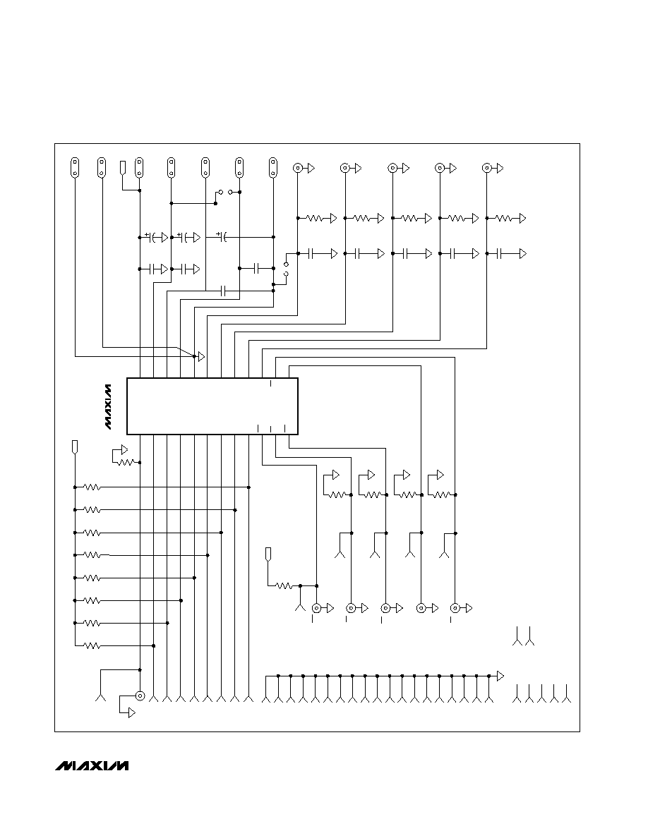
Table 1. Jumper Functions
Table 2. 40-Pin Header (J1) Signals
JUMPER
STATE
FUNCTION
JU1
Open
REFADJ pin open or driven externally
Shorted
REFADJ pin shorted to V
DD
*
JU2
Open
COM pin open or driven externally
Shorted
COM pin shorted to AGND
*The MAX1292's 2.5V reference must be disabled before an
external reference voltage is connected. Installing a shunt
across JU1 connects the REFADJ pin to V
DD
and disables the
on-board reference.
14
PIN NUMBER
SIGNAL
D6
2
D0/D8
16
4
D1/D9
D7
6
D2/D10
18
8
D3/D11
HBEN
10
D4
20
12
D5
INT
22
RD
24
WR
26
CLK
1, 3, 5, 7, 9, 11, 13, 15,
17, 19, 21, 23, 25, 27, 29,
31, 33, 35, 37, 39
GND
28
CS
30, 32, 34, 36, 38, 40
N.C.
Evaluates: MAX1292/MAX1293
MAX1292 Evaluation Kit
_______________________________________________________________________________________
3
24
23
22
21
20
19
18
17
1
2
3
4
5
6
7
8
D5
D6
D7
HBEN
D1/D9
D2/D10
D3/D11
D4
16
15
14
13
9
10
11
12
V
LOGIC
V
DD
REF
REFADJ
GND
COM
CH0
CH1
CH2
CH3
CLK
D0/D8
MAX1292
AGND
VLOGIC
DGND
VDD
REF
REFADJ
RGND
COM
CH0
CH1
CH2
CH3
VLOGIC
R12
51
R8
51
R9
51
R10
51
R11
51
C11
0.1
µ
F
C7
0.01
µ
F
C6
0.01
µ
F
C5
4.7
µ
F
10V
C4
4.7
µ
F
10V
C3
0.1
µ
F
C1
0.1
µ
F
C2
4.7
µ
F
10V
C10
0.1
µ
F
C9
0.1
µ
F
C8
0.1
µ
F
C12
0.1
µ
F
JU2
INT
RD
CS
WR
R2
51
R1H
47k
R1G
47k
R1F
47k
R1E
47k
R1D
47k
R1C
47k
R1B
47k
R1A
47k
9
8
7
65432
V
LOGIC
J118
J116
J114
J112
J110
J18
J16
J14
J12
J120
J11
J13
J15
J17
J19
J111
J113
J115
J117
J1 19
J121
J123
J125
J127
J129
J131
J133
J135
J137
J139
J140
J136
J138
J130
J132
J134
J122
J124
J126
J128
HBEN
R1-1
47k
R4
51
R5
51
R6
51
R7
51
V
LOGIC
CLK
INT
RD
CS
WR
N.C.
N.C.
N.C.
N.C.
N.C.
N.C.
N.C.
10
U1
JU1
Figure 1. MAX1292 EV Kit Schematic
Evaluates: MAX1292/MAX1293
MAX1292 Evaluation Kit
4
_______________________________________________________________________________________
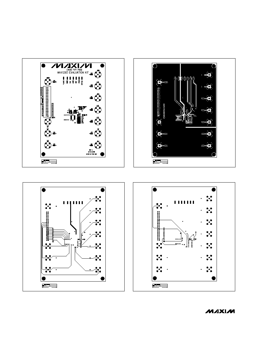
Figure 2. MAX1292 EV Kit Component Placement Guide--
Component Side
1.0"
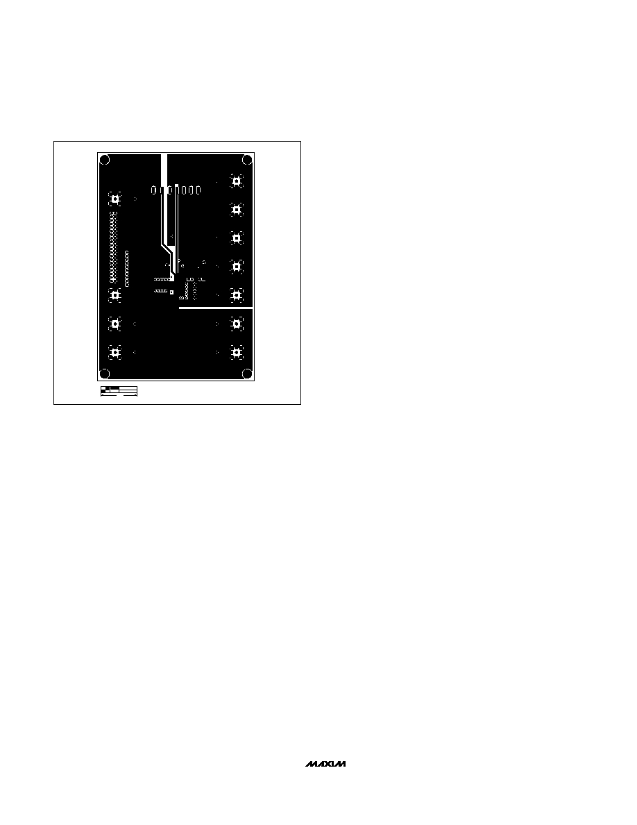
Figure 3. MAX1292 EV Kit PC Board Layout--Component Side
1.0"
Figure 5. MAX1292 EV Kit PC Board Layout--Interior Layer 2
1.0"
Figure 4. MAX1292 EV Kit PC Board Layout--Interior Layer 1
1.0"
Maxim cannot assume responsibility for use of any circuitry other than circuitry entirely embodied in a Maxim product. No circuit patent licenses are
implied. Maxim reserves the right to change the circuitry and specifications without notice at any time.
Maxim Integrated Products, 120 San Gabriel Drive, Sunnyvale, CA 94086 408-737-7600 _____________________ 5
© 1999 Maxim Integrated Products
Printed USA
is a registered trademark of Maxim Integrated Products.
Figure 6. MAX1292 EV Kit PC Board Layout--Solder Side
1.0"
Evaluates: MAX1292/MAX1293
MAX1292 Evaluation Kit