General Description
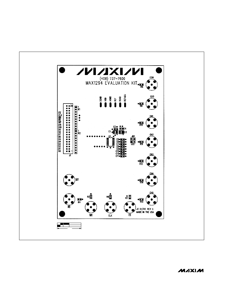
The MAX1294 evaluation kit (EV kit) is assembled with a
MAX1294 and the basic components necessary to
evaluate the 12-bit analog-to-digital converter (ADC).
Connectors for power supplies, analog inputs, and digi-
tal signals simplify connections to the device. A 40-pin
header allows the user to connect a logic analyzer
using a ribbon cable or the conventional miniclips. BNC
connectors with 50
termination provide easy connec-
tion between function generators and the analog inputs.
The board layout is designed to yield 12-bit accuracy
with low noise when sampling at the maximum rate of
420ksps.
The MAX1294 EV kit may also be used to evaluate the
MAX1295. Request a free sample of the MAX1295BCEI
when ordering the MAX1294 EV kit.
Features
o 12-Bit Analog-to-Digital Conversion
o Six Input Channels
o 12-Bit-Wide Digital Interface
o Internal Track and Hold
o 420kHz Sampling Rate
o Internal 2.5V Reference
o Internal Clock
o Low-Power Standby Mode
o Fully Assembled Surface-Mount Board
Quick Start
The MAX1294 EV kit comes fully assembled and tested.
The following equipment is required:
∑ A +5V linear power supply (switching supplies will in-
duce excess noise on the power input)
∑ A low-distortion function generator
∑ A logic analyzer
A logic analyzer or other digital system is needed to
provide the clock and control signals and to capture
the conversion results of the MAX1294. Connect the
logic analyzer using a 40-pin ribbon cable or a combi-
nation of BNC cables, ribbon cable, and miniclips.
Refer to the MAX1294 data sheet for detailed informa-
tion on timing requirements.
The analog input signals must be delivered by a low-
distortion source to achieve full 12-bit accuracy. All
analog channels connect to BNC connectors terminat-
ed with 51
resistors. For best low-noise performance,
maintain separate analog and digital supplies and
grounds to the board. The grounds are connected in a
star configuration centered on the ground plane of the
board. Refer to the MAX1294/MAX1296 data sheet for a
detailed discussion of signal grounds.
Many of the digital and analog signals on the evaluation
kit have 51
termination resistors matching typical gen-
erator impedance. These should be removed if high-
impedance sources are used.
Evaluates: MAX1294/MAX1295
MAX1294 Evaluation Kit
________________________________________________________________ Maxim Integrated Products
1
19-1646; Rev 0; 2/00
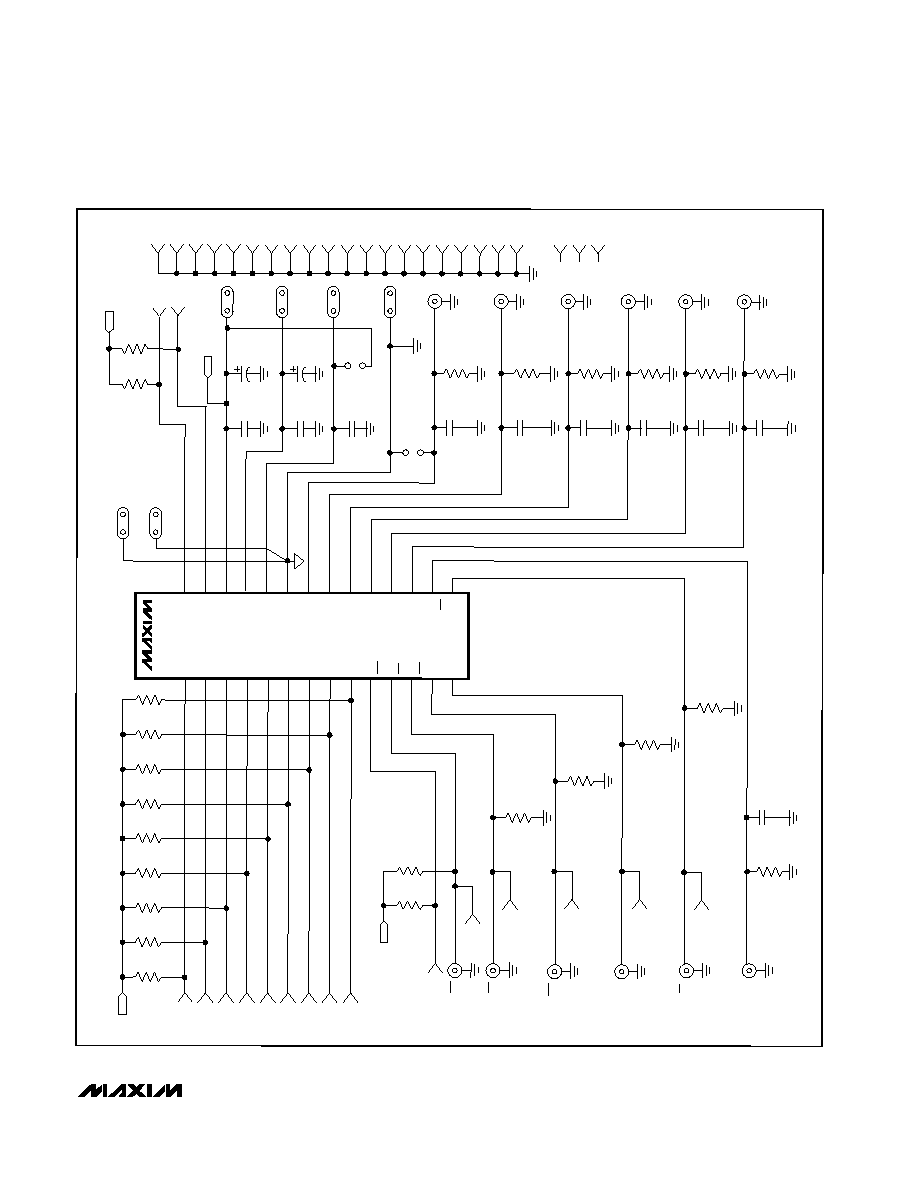
Component List
PART
MAX1294EVKIT
0∞C to +70∞C
TEMP. RANGE
IC PACKAGE
28 QSOP
Ordering Information
MAX1294 printed circuit board
1
None
Shunts
2
None
MAX1294BCEI
1
U1
51
±5% resistors
11
R4≠R14
47k
, 9-resistor, 10-pin SIPs
2
R1, R2
2-pin headers
2
JU1, JU2
DESIGNATION
40-pin header
1
J1
BNC connectors
12
INT, RD, WR,
CLK, CS, COM,
CH0-CH5
0.01µF ceramic capacitors
2
C4, C5
4.7µF, 10V tantalum capacitors
AVX TAJB475M010R
2
C1, C3
DESCRIPTION
QTY
MAX1294 data sheet
1
None
0.1µF ceramic capacitors
8
C2, C6≠C12
For free samples and the latest literature, visit www.maxim-ic.com or phone 1-800-998-8800.
For small orders, phone 1-800-835-8769.
Evaluates: MAX1294/MAX1295
MAX1294 Evaluation Kit
2
_______________________________________________________________________________________
Connections and Setup
Connect all supplies and signal lines before turning on
any supply or signal source:
1) Connect a +5V power supply to the VDD pad.
Connect the ground to the AGND pad. The DGND
provides additional access to the digital ground
plane.
2) Make sure there is no shunt installed on JU1 (Table 1).
This enables the internal 2.5V reference.
3) Connect the analog source (function generators or
user signals) to the analog input channels (CH0≠
CH5). Install a shunt on JU2 to connect the COM pin
to GND.
4) Connect a logic analyzer, word generator, or other
source for the digital data lines D0≠D11. These sig-
nals are available on the 40-pin header (Table 2).
5) Connect the digital control signals for CS, RD, and
WR. These signals are available on the 40-pin head-
er or on BNC connectors.
6) Connect the clock signal (0.1MHz to 7.6MHz) to the
CLK BNC connector or leave the pin open to use the
internal clock.
7) Turn on the VDD supply, then enable the digital sig-
nal source.
8) Turn on the analog sources, and the system is ready
for use.
9) Use the logic analyzer for data analysis.
Detailed Description
Analog Input Signals
The analog inputs are configured for using a function
generator. The inputs have 51
loads and 0.1µF
capacitors to match the generator's impedance. It may
be necessary to remove these if the board is connected
to the user's system. The system must provide low
impedance and any necessary anti-aliasing filtering.
Grounding
The MAX1294 evaluation board uses two separate
ground planes to reduce noise. All digital signals con-
nect to the digital ground plane (DGND), and the
noise-sensitive analog signals connect to the separate
analog ground plane (AGND). The two grounds con-
nect at only one point near the ground pin (pin 23) of
the MAX1294. The ground connection (RGND) for the
optional external reference supply is connected direct-
ly to the same point. This "star" ground configuration is
common in low-noise analog systems.
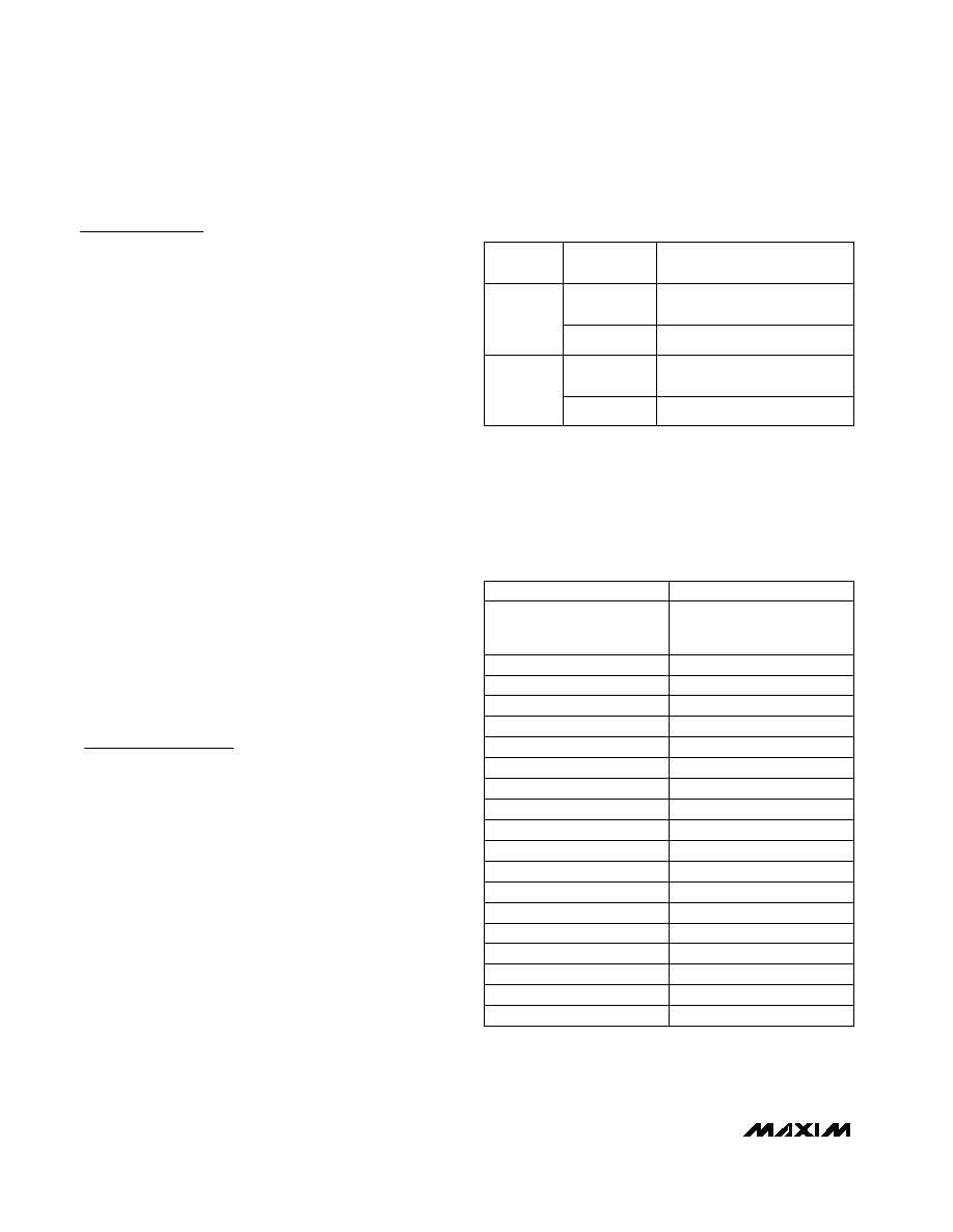
SHUNT
LOCATION
SHDN PIN
MAX1294 OUTPUT
Open
REFADJ pin open or driven
externally
Open
COM pin open or driven exter-
nally
Shorted
REFADJ pin shorted to VDD*
Shorted
COM pin shorted to AGND
JU1
JU2
*The MAX1294's 2.5V reference must be disabled before an
external reference voltage is connected. Installing a shunt
across JU1 connects the REFADJ pin to VDD and disables the
on-board reference.
Table 2. 40-Pin Header (J1) Signals
PIN
SIGNAL
1, 3, 5, 7, 9, 11, 13, 15, 17, 19,
21, 23, 25, 27, 29, 31, 33, 35,
37, 39
GND
2
D0
4
D1
6
D2
8
D3
10
D4
12
D5
14
D6
16
D7
18
D8
20
D9
22
D10
24
D11
26
INT
28
RD
30
WR
32
CLK
34
CS
36, 38, 40
N.C.
Table 1. Jumper Functions