MAX13481E-83E DS
General Description
The MAX13481E/MAX13482E/MAX13483E ±15kV ESD-
protected USB-compliant transceivers interface low-
voltage ASICs with USB devices. The transceivers fully
comply to USB 2.0 when operating at full-speed
(12Mbps). The transceivers also operate with V
L
as low
as 1.6V, ensuring compatibility with low-voltage ASICs.
The MAX13481E/MAX13482E/MAX13483E feature a
logic-selectable suspend mode that reduces current
consumption. Integrated ±15kV ESD circuitry protects
D+ and D- bus connections.
The MAX13481E/MAX13482E/MAX13483E operate over
the extended -40°C to +85°C temperature range and are
available in a 16-pin (3mm x 3mm) thin QFN package.
Applications
Cell Phones
PDAs
Digital Still Cameras
Features
Active-Low Enumeration Input Controls D+ Pullup
Resistor (MAX13482E)
Active-Low Enumeration Input Controls Internal
Pullup Switch (MAX13481E)
±15kV ESD Protection on D+ and D-
USB 2.0 Full-Speed Compliant Transceiver
V
BUS
Detection (MAX13482E/MAX13483E)
+1.60V to +3.6V V
L
Allows Connection with Low-
Voltage ASICs
No Power-Supply Sequencing Required
Pin Compatible with MIC2551A (MAX13481E)
Pin Compatible with DP1680 (MAX13483E)
Pin Compatible with DP1681 (MAX13481E)
Pin Compatible with DP1682 (MAX13482E)
MAX13481E/MAX13482E/MAX13483E
±15kV ESD-Protected USB Transceivers with
External/Internal Pullup Resistors
________________________________________________________________ Maxim Integrated Products
1
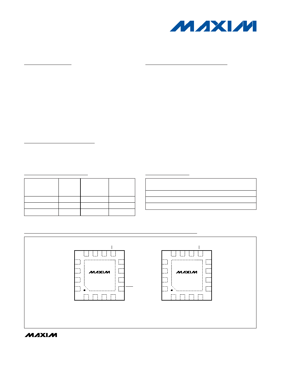
TOP VIEW
15
16
14
13
5
6
7
VP
VM
8
N.C.
D-
OE
V
TRM
1
3
V
BUS
4
12
10
9
V
L
BD
N.C.
SUS
GND
N.C.
*EP
MAX13483E
RCV
D+
2
11
I.C.
TQFN
3mm x 3mm
15
16
14
13
5
6
7
VP
VM
8
SP (N.C.)
D-
OE
V
TRM
1
3
V
BUS
4
12
10
9
V
L
N.C. (BD)
N.C.
SUS
GND
ENUM
*EP
MAX13481E
MAX13482E
RCV
D+
2
11
VPU (VPUR)
TQFN
3mm x 3mm
*EXPOSED PADDLE
*EXPOSED PADDLE
( ) MAX13482E ONLY
Pin Configurations
Ordering Information
Selector Guide
PART
PIN-PACKAGE
TOP
MARK
PKG
CODE
MAX13481EETE
3mm X 3mm TQFN-EP*
ADF
T1633-4
MAX13482EETE
3mm X 3mm TQFN-EP*
ADI
T1633-4
MAX13483EETE
3mm X 3mm TQFN-EP*
ADJ
T1633-4
PART
ENUM
INPUT
INTERNAL
1.5k
RESISTOR
V
BUS
DETECTION
MAX13481EETE
--
--
MAX13482EETE
MAX13483EETE
--
--
19-3801; Rev 2; 1/06
For pricing, delivery, and ordering information, please contact Maxim/Dallas Direct! at
1-888-629-4642, or visit Maxim's website at www.maxim-ic.com.
Typical Operating Circuits appear at end of data sheet.
*EP = Exposed Paddle.
MAX13481E/MAX13482E/MAX13483E
±15kV ESD-Protected USB Transceivers with
External/Internal Pullup Resistors
2
_______________________________________________________________________________________
ABSOLUTE MAXIMUM RATINGS
ELECTRICAL CHARACTERISTICS
(V
CC
= +4V to +5.5V, V
L
= +1.6V to +3.6V, T
A
= T
MIN
to T
MAX
, unless otherwise noted. Typical values are at V
CC
= +5V, V
L
= +2.5V,
T
A
= +25°C.) (Note 1)
Stresses beyond those listed under "Absolute Maximum Ratings" may cause permanent damage to the device. These are stress ratings only, and functional
operation of the device at these or any other conditions beyond those indicated in the operational sections of the specifications is not implied. Exposure to
absolute maximum rating conditions for extended periods may affect device reliability.
(All voltages referenced to GND, unless otherwise noted.)
V
BUS
, V
L,
..................................................................-0.3V to +7V
V
TRM
, VPUR, VPU .....................................-0.3V to (V
BUS
+ 0.3V)
Input Voltage (D+, D-) ..............................................-0.3V to +7V
VM, VP, SUS, RCV,
ENUM, BD, OE, ............-0.3V to (V
L
+ 0.3V)
Short-Circuit Current to V
CC
or GND (D+, D-)... ........... ±150mA
Maximum Continuous Current (all other pins) ..................±15mA
Continuous Power Dissipation (T
A
= +70
°C)
16-Pin, 3mm x 3mm TQFN (derate 15.6mW/
°C above
+70
°C).......................................................................1250mW
Operating Temperature Range ...........................-40
°C to +85°C
Junction Temperature ......................................................+150
°C
Storage Temperature Range .............................-65
°C to +150°C
Lead Temperature (soldering, 10s) .................................+300
°C
PARAMETER
SYMBOL
CONDITIONS
MIN
TYP
MAX
UNITS
SUPPLY INPUTS (V
BUS
, V
TRM
, V
L
)
V
BUS
Input Range
V
BUS
4.0
5.5
V
V
L
Input Range
V
L
1.6
3.6
V
Regulated Supply-Voltage Output
V
VTRM
3.0
3.3
3.6
V
Operating V
CC
Supply Current
I
VCC
Full-speed transmitting/receiving at
12Mbps, C
L
= 50pF on D+ and D- (Note 2)
10
mA
Operating V
L
Supply Current
I
VL
Full-speed transmitting/receiving at
12Mbps, C
L
= 15pF receiver outputs,
V
L
= 2.5V (Note 2)
2.5
mA
Full-speed idle, V
D+
> 2.7V, V
D-
< 0.3V
250
350
Full-Speed Idle and SE0 Supply
Current
I
VCC(IDLE)
SE0: V
D+
< 0.3V, V
D-
< 0.3V
250
350
µA
Static V
L
Supply Current
I
VL(STATIC)
Full-speed idle, SE0 or suspend mode
5
µA
Suspend Supply Current
I
VCC(SUSP)
VM = VP = open,
ENUM = SUS = OE = high
35
µA
Disabled-Mode Supply Current
I
VCC(DIS)
V
L
= GND or open
20
µA
Sharing-Mode V
L
Supply Current
I
V L(S H ARIN G)
V
BUS
= GND or open,
OE = low,
VP = low or high, VM = low or high, SUS =
high,
ENUM = high
5
µA
Disable-Mode Load Current on
D+ and D-
I
D X (D IS ABLE )
V
L
= GND or open, V
D_
= 0 or 5.5V
5
µA
Sharing-Mode Load Current on
D+ and D-
I
DX (SH ARING)
V
BUS
= GND or open, V
D_
= 0 or 5.5V
20
µA
V
TH_H
Supply present
3.6
V
L
1.7V
0.8
USB Power-Supply Detection
Threshold
V
TH_L
Supply lost
V
L
< 1.7V
0.7
V
USB Power-Supply Detection
Hysteresis
V
HYST
75
mV
V
L
Supply-Voltage Detection
Threshold
V
TH(VL)
0.85
V
MAX13481E/MAX13482E/MAX13483E
±15kV ESD-Protected USB Transceivers with
External/Internal Pullup Resistors
_______________________________________________________________________________________
3
ELECTRICAL CHARACTERISTICS (continued)
(V
CC
= +4V to +5.5V, V
L
= +1.6V to +3.6V, T
A
= T
MIN
to T
MAX
, unless otherwise noted. Typical values are at V
CC
= +5V, V
L
= +2.5V,
T
A
= +25°C.) (Note 1)
PARAMETER
SYMBOL
CONDITIONS
MIN
TYP
MAX
UNITS
ANALOG VOLTAGE OUTPUTS (VPU, VPUR)
Off-State Leakage
I
LZ
ENUM = V
L
-1
+1
µA
VPU Switch Resistance
MAX13481E
10
VPUR Pullup Resistance
MAX13482 (Note 3)
1.425
1.575
k
DIGITAL INPUTS/OUTPUTS (VP,VM, RCV,
OE, ENUM, SUS, BD)
Input-High Voltage
V
IH
VP, VM,
OE, ENUM, SUS
0.7 x V
L
V
Input-Low Voltage
V
IL
VP, VM,
OE, ENUM, SUS
0.3 x V
L
V
Output Voltage High
V
OH
VP, VM, RCV, BD, I
SOURCE
= 2mA
V
L
- 0.4
V
Output Voltage Low
V
OL
VP, VM, RCV, BD, I
SINK
= 2mA
0.4
V
Input Leakage Current
I
LKG
-1
+1
µA
Input Capacitance
Measured from input to GND
10
pF
ANALOG INPUT/OUTPUTS (D+, D-)
Differential Input Sensitivity
V
DI
|(V
D+
- V
D-
)|
200
mV
Differential Common-Mode
Voltage Range
V
CM
Include V
DI
0.8
2.5
V
Single-Ended Input-Low Voltage
V
IL
0.8
V
Single-Ended Input-High Voltage
V
IH
2.0
V
Hysteresis
V
HYS
250
mV
Output Voltage Low
V
OL
R
L
= 1.5k
from D+ or D- to 3.6V
0.3
V
Output Voltage High
V
OH
R
L
= 15k
to GND
2.8
3.6
V
Off-State Leakage Current
Three-state driver
-1
+1
µA
Transceiver Capacitance
C
IND
D_ to GND
20
pF
Driver Output Impedance
R
OUT
2
15
ESD PROTECTION (D+, D-)
Human Body Model
±15
kV
IEC 61000-4-2 Contact Discharge
±8
kV
TIMING CHARACTERISTICS
(V
CC
= +4V to +5.5V, V
L
= +1.6V to +3.6V, T
A
= T
MIN
to T
MAX
, unless otherwise noted. Typical values are at V
CC
= +5V, V
L
= +2.5V,
T
A
= +25°C.) (Note 1)
PARAMETER
SYMBOL
CONDITIONS
MIN
TYP
MAX
UNITS
DRIVER CHARACTERISTICS (C
L
= 50pF)
Rise Time D+/D-
t
FR
10% to 90% of |V
OH
-V
OL
| (Figures 1, 9)
4
20
ns
Fall Time D+/D-
t
FF
90% to 10% of |V
OH
-V
OL
| (Figures 1, 9)
4
20
ns
Rise- and Fall-Time Matching
t
FR
/t
FF
Excluding the first transition from idle state,
(Figure 1) (Note 2)
90
110
%
MAX13481E/MAX13482E/MAX13483E
±15kV ESD-Protected USB Transceivers with
External/Internal Pullup Resistors
4
_______________________________________________________________________________________
PARAMETER
SYMBOL
CONDITIONS
MIN
TYP
MAX
UNITS
Output Signal Crossover Voltage
V
CRS
(Figure 2) (Note 2)
1.3
2
V
t
PLH_DRV
Low-to-high transition (Figure 2)
18
ns
Driver Propagation Delay
t
PHL_DRV
High-to-low transition (Figure 2)
18
ns
t
PZH_DRV
Off-to-high transition (Figures 3, 10)
20
ns
Driver-Enabled Delay Time
t
PZL_DRV
Off-to-low transition (Figures 3, 10)
20
ns
t
PHZ_DRV
High-to-off transition (Figures 3, 10)
20
ns
Driver Disabled Delay
t
PLZ_DRV
Low-to-off transition (Figures 3, 10)
20
ns
RECEIVER (C
L
= 15pF)
t
PLH_RCV
Low-to-high transition (Figures 4, 9)
20
Differential Receiver
Propagation Delay
t
PHL_RCV
High-to-low transition (Figures 4, 9)
20
ns
t
PLH_SE
Low-to-high transition (Figures 4, 9)
12
Single-Ended Receiver
Propagation Delay
t
PHL_SE
High-to-low transition (Figures 4, 9)
12
ns
t
PHZ_SE
High-to-off transition (Figure 5)
15
Single-Ended Receiver Disable
Delay
t
PLZ_SE
Off-to-low transition (Figure 5)
15
ns
t
PZH_SE
Off-to-high transition (Figure 5)
15
Single-Ended Receiver Enable
Delay
t
PZL_SE
Off-to-low transition (Figure 5)
15
ns
TIMING CHARACTERISTICS (continued)
(V
CC
= +4V to +5.5V, V
L
= +1.6V to +3.6V, T
A
= T
MIN
to T
MAX
, unless otherwise noted. Typical values are at V
CC
= +5V, V
L
= +2.5V,
T
A
= +25°C.) (Note 1)
Note 1: Parameters are 100% production tested at +25°C, unless otherwise noted. Limits over temperature are guaranteed by
design.
Note 2: Guaranteed by design, not production tested.
Note 3: Including external 27
series resistor.
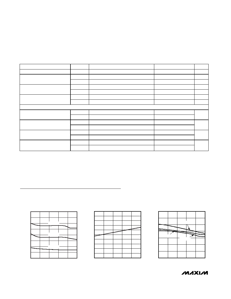
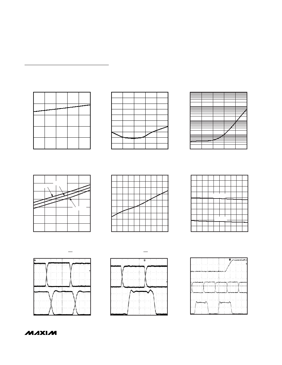
DIFFERENTIAL RECEIVER
PROPAGATION DELAY vs. V
L
V
L
(V)
PROPAGATION DELAY (ns)
MAX13481E toc01
1.6
2.0
2.4
2.8
3.2
3.6
10.0
10.5
11.0
11.5
12.0
12.5
13.0
13.5
14.0
T
A
= +85
°C
T
A
= +25
°C
T
A
= -40
°C
DIFFERENTIAL RECEIVER PROPAGATION
DELAY vs. TEMPERATURE
TEMPERATURE (
°C)
PROPAGATION DELAY (ns)
MAX13481E toc02
-40
-15
10
35
60
85
6
7
8
9
10
11
12
13
14
15
16
SINGLE-ENDED RECEIVER PROPAGATION
DELAY vs. V
L
V
L
(V)
PROPAGATION DELAY (ns)
MAX13481 toc03
1.6
2.0
2.4
2.8
3.2
3.6
0
1
2
3
4
5
6
7
T
A
= +85
°C
T
A
= +25
°C
T
A
= -40
°C
Typical Operating Characteristics
(V
BUS
= 5V, V
L
= +3.3V, T
A
= +25°C, unless otherwise noted.)
MAX13481E/MAX13482E/MAX13483E
±15kV ESD-Protected USB Transceivers with
External/Internal Pullup Resistors
_______________________________________________________________________________________
5
SINGLE-ENDED RECEIVER PROPAGATION
DELAY vs. TEMPERATURE
TEMPERATURE (
°C)
PROPAGATION DELAY (ns)
MAX13481E toc04
-40
-15
10
35
60
85
0
1
2
3
4
5
TRANSMITTER SKEW
vs. TEMPERATURE
TEMPERATURE (
°C)
TRANSMITTER SKEW (ns)
MAX13481E toc05
-40
-15
10
35
60
85
0
0.2
0.4
0.6
0.8
1.0
1.2
1.4
1.6
1.8
2.0
100
0.01
-40
-15
35
85
60
V
L
SUSPEND CURRENT
vs. TEMPERATURE
0.1
1
10
MAX13481E toc06
TEMPERATURE (
°C)
V
L
SUSPEND CURRENT (
A)
10
V
BUS
SUSPEND CURRENT
vs. V
BUS
V
BUS
(V)
V
BUS
SUPPLY CURRENT (
A)
MAX13481E toc07
4.0
4.3
4.6
4.9
5.2
5.5
13
14
15
16
17
18
19
20
T
A
= +85
°C
T
A
= +25
°C
T
A
= -40
°C
0
4
2
8
6
10
12
16
14
18
0 10 20 30 40 50 60 70 80 90 100
V
BUS
SUPPLY CURRENT
vs. D+/D- CAPACITANCE
MAX13481E toc08
CAPACITANCE (pF)
V
BUS
SUPPLY CURRENT (mA)
1.00
1.10
1.05
1.20
1.15
1.25
1.30
1.40
1.45
1.35
1.50
0 10 20 30 40 50 60 70 80 90 100
V
L
SUPPLY CURRENT
vs. D+/D- CAPACITANCE
MAX13481E toc09
CAPACITANCE (pF)
V
BUS
SUPPLY CURRENT (mA)
V
L
= 2.5V
V
L
= 1.8V
Typical Operating Characteristics (continued)
(V
BUS
= 5V, V
L
= +3.3V, T
A
= +25°C, unless otherwise noted.)
TRANSMIT MODE (OE = LOW)
MAX13481E toc10
1V/div
1V/div
D-
D+
VM
VP
10ns/div
RECEIVE MODE (OE = HIGH)
MAX13481E toc11
1V/div
RCV
1V/div
D-
D+
10ns/div
SUSPEND MODE
MAX13481E toc12
D-
D+
SUS
2V/div
RCV
2V/div
20ns/div
2V/div