 | –≠–ª–µ–∫—Ç—Ä–æ–Ω–Ω—ã–π –∫–æ–º–ø–æ–Ω–µ–Ω—Ç: MAX1367 | –°–∫–∞—á–∞—Ç—å:  PDF PDF  ZIP ZIP |
General Description
The MAX1365/MAX1367 low-power, 4.5- and 3.5-digit,
panel meters feature an integrated sigma-delta analog-
to-digital converter (ADC), LED display drivers, voltage
digital-to-analog converter (DAC), and a 4≠20mA
(or 0 to 16mA) current driver.
The MAX1365/MAX1367's analog input voltage range is
programmable to either ±2V or ±200mV. The MAX1367
drives a 3.5-digit (±1999 count) display and the
MAX1365 drives a 4.5-digit (±19,999 count) display.
The ADC output directly drives the LED display as well
as the voltage DAC, which in turn drives the 4≠20mA
(or 0 to 16mA) current-loop output.
In normal operation, the 0 to 16mA/4≠20mA current-
loop output follows the ±2V or ±200mV analog input to
drive remote panel-meter displays, data loggers, and
other industrial controllers. For added flexibility, the
MAX1365/MAX1367 allow direct access to the DAC
output and the V/I converter input.
The sigma-delta ADC does not require external preci-
sion integrating capacitors, autozero capacitors, crystal
oscillators, charge pumps, or other circuitry commonly
required in dual-slope ADC panel-meter circuits. On-
chip analog input and reference buffers allow direct
interface with high-impedance signal sources. Excellent
common-mode rejection and digital filtering provide
greater than 100dB rejection of simultaneous 50Hz and
60Hz line noise. Other features include data hold, peak
detection, and overrange/underrange detection.
The MAX1365/MAX1367 require a 2.7V to 5.25V supply,
a 4.75V to 5.25V V/I supply, and a 7V to 30V loop sup-
ply. They are available in a space-saving (7mm x
7mm), 48-pin TQFP package and operate over the
extended (-40∞C to +85∞C) temperature range.
Applications
Automated Test Equipment
Data-Acquisition Systems
Digital Multimeters
Digital Panel Meters
Digital Voltmeters
Industrial Process Control
Features
Stand-Alone, Digital Panel Meter
20-Bit Sigma-Delta ADC
4.5-Digit Resolution (±19,999 Count, MAX1365)
3.5-Digit Resolution (±1999 Count, MAX1367)
No Integrating/Autozeroing Capacitors
100M
Input Impedance
±200mV or ±2.000V Input Range
LED Display
Common-Cathode 7-Segment LED Driver
Programmable LED Current (0 to 20mA)
2.5Hz Update Rate
Output DAC and Current Driver
±15-Bit DAC with 14-Bit Linear V/I Converter
Selectable 0 to 16mA or 4≠20mA Current Output
Unipolar/Bipolar Modes
±50µA Zero Scale, ±40ppmFS/∞C (typ)
±0.5% Gain Error, ±25ppmFS/∞C (typ)
Separate 7V to 30V Supply for Current-Loop
Output
2.7V to 5.25V ADC/DAC Supply
4.75V to 5.25V V/I Converter Supply
Internal 2.048V Reference or External Reference
48-Pin, 7mm x 7mm TQFP Package
MAX1365/MAX1367
Stand-Alone, 4.5-/3.5-Digit Panel Meters
with 4≠20mA Output
________________________________________________________________ Maxim Integrated Products
1
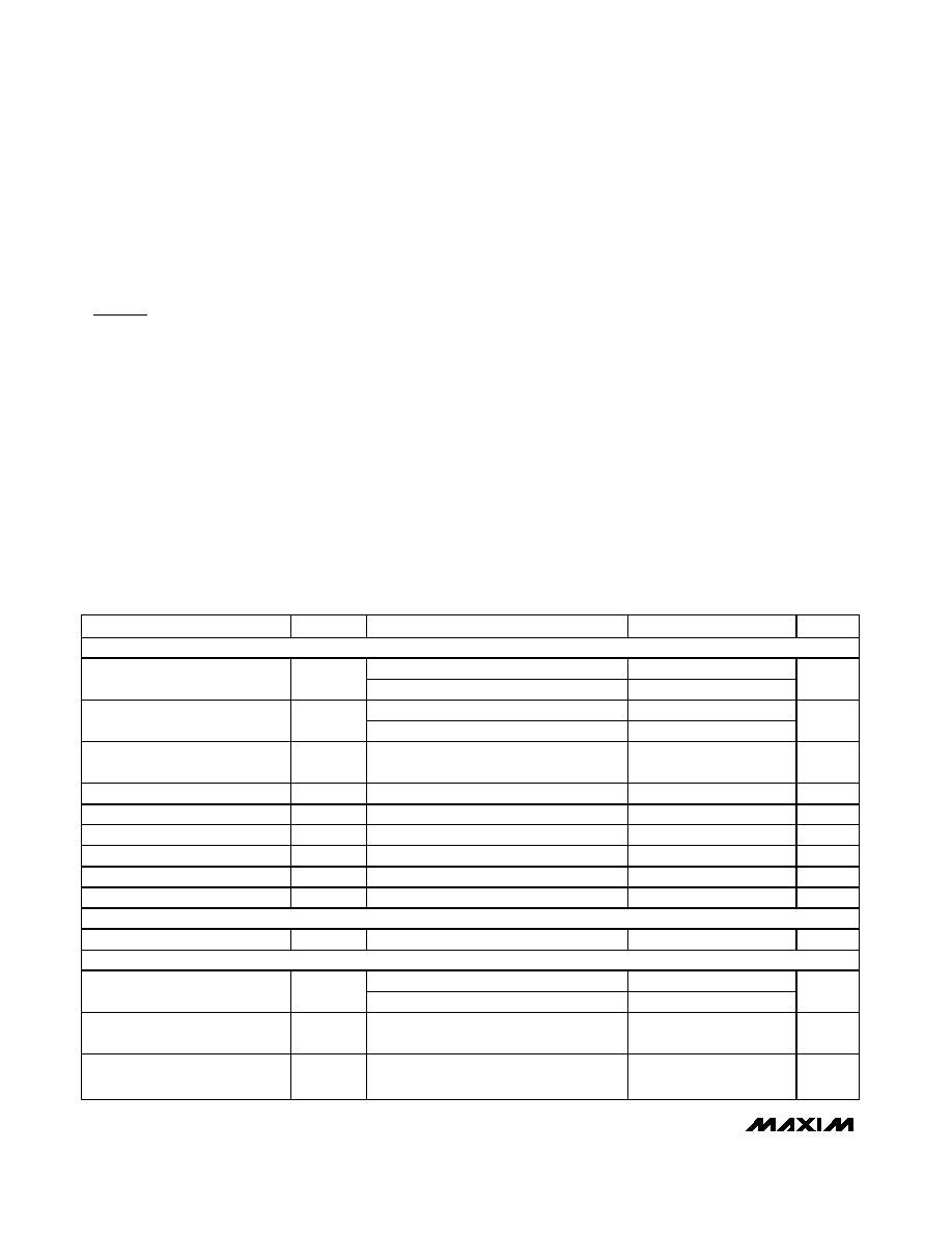
Selector Guide
19-3889; Rev 1; 1/06
For pricing, delivery, and ordering information, please contact Maxim/Dallas Direct! at
1-888-629-4642, or visit Maxim's website at www.maxim-ic.com.
PART
TEMP RANGE
PIN-PACKAGE
MAX1365ECM
-40∞C to +85∞C
48 TQFP
MAX1367ECM
-40∞C to +85∞C
48 TQFP
Ordering Information
PART
RESOLUTION
(DIGITS)
PKG
CODE
MAX1365ECM
4.5
C48-6
MAX1367ECM
3.5
C48-6
Pin Configuration appears at end of datasheet.
Typical Operating Circuits appear at end of datasheet.
MAX1365/MAX1367
Stand-Alone, 4.5-/3.5-Digit Panel Meters
with 4≠20mA Output
2
_______________________________________________________________________________________
ABSOLUTE MAXIMUM RATINGS
ELECTRICAL CHARACTERISTICS
(AV
DD
= DV
DD
= DAC_VDD = +2.7V to +5.25V, GND = 0, V
LEDV
= +2.7V to +5.25V, LEDG = 0, V
REF+
- V
REF-
= 2.048V (external
reference), 4-20OUT = 7V, V
REG_AMP
= +5.0V, C
REF+
= 0.1µF, REF- = GND, C
NEGV
= 0.1µF. Internal clock mode, unless otherwise
noted. All specifications are at T
A
= T
MIN
to T
MAX
. Typical values are at T
A
= +25∞C, unless otherwise noted.)
Stresses beyond those listed under "Absolute Maximum Ratings" may cause permanent damage to the device. These are stress ratings only, and functional
operation of the device at these or any other conditions beyond those indicated in the operational sections of the specifications is not implied. Exposure to
absolute maximum rating conditions for extended periods may affect device reliability.
AV
DD,
DV
DD ....................................................................
-0.3V to +6.0V
AIN+, AIN-, REF+, REF-.........................V
NEGV
to (AV
DD
+ 0.3V)
REG_FORCE, CMP, DAC_VDD, DACVOUT,
CONV_IN, 4-20OUT .............................-0.3V to (AV
DD
+ 0.3V)
EN_BPM, EN_I, REFSELE, DACDATA_SEL, INTREF, RANGE,
DPSET1, DPSET2, HOLD, PEAK, DPON,
CS_DAC...............................................-0.3V to (DV
DD
+ 0.3V)
NEGV .......................................................-2.6V to (AV
DD
+ 0.3V)
LED_EN....................................................-0.3V to (DV
DD
+ 0.3V)
SET...........................................................-0.3V to (AV
DD
+ 0.3V)
REG_AMP, REG_VDD ...........................................-0.3V to +6.0V
LEDV......................................................................-0.3V to +6.0V
LEDG .....................................................................-0.3V to +0.3V
GND_DAC .............................................................-0.3V to +0.3V
GND_V/I.................................................................-0.3V to +0.3V
SEG_ to LEDG.........................................-0.3V to (V
LEDV
+ 0.3V)
DIG_ to LEDG..........................................-0.3V to (V
LEDV
+ 0.3V)
REF_DAC .................................................-0.3V to (AV
DD
+ 0.3V)
DIG_ Sink Current .............................................................300mA
DIG_ Source Current...........................................................50mA
SEG_ Sink Current . ............................................................50mA
SEG_ Source Current..........................................................50mA
Maximum Current Input into Any Other Pin . ......................50mA
Continuous Power Dissipation (T
A
= +70∞C)
48-Pin TQFP (derate 22.7mW/∞C above +70∞C).....1818.2mW
Operating Temperature Range ...........................-40∞C to +85∞C
Storage Temperature Range .............................-60∞C to +150∞C
Junction Temperature ......................................................+150∞C
Lead Temperature (soldering, 10s) .................................+300∞C
PARAMETER
SYMBOL
CONDITIONS
MIN
TYP
MAX
UNITS
ADC ACCURACY
MAX1365
-19,999
+19,999
Noise-Free Resolution
MAX1367
-1999
+1999
Counts
2.000V range
±1
Integral Nonlinearity (Note 1)
INL
200mV range
±1
Counts
Range Change Ratio
(V
AIN+
- V
AIN-
= 0.100V) on 200mV range;
(V
AIN+
- V
AIN-
= 0.100V) on 2.0V range
10:1
Ratio
Rollover Error
V
AIN+
- V
AIN-
= full scale
±1
Counts
Output Noise
10
µV
P-P
Offset Error (Zero Input Reading)
V
AIN+
- V
AIN-
= 0 (Note 2)
-0
+0
Counts
Gain Error
(Note 3)
-0.5
+0.5
%FSR
Offset Drift (Zero Reading Drift)
V
AIN+
- V
AIN-
= 0 (Note 4)
0.1
µV/∞C
Gain Drift
±1
ppm/∞C
INPUT CONVERSION RATE
Update Rate
5
Hz
ANALOG INPUTS (AIN+, AIN-) (bypass to GND with 0.1µF or greater capacitors)
RANGE = GND
-2.0
+2.0
AIN Input Voltage Range (Note 5)
RANGE = DV
DD
-0.2
+0.2
V
AIN Absolute Input Voltage
Range to GND
-2.2
+2.2
V
Normal-Mode 50Hz and 60Hz
Rejection (Simultaneously)
50Hz and 60Hz ±2%
100
dB
MAX1365/MAX1367
Stand-Alone, 4.5-/3.5-Digit Panel Meters
with 4≠20mA Output
_______________________________________________________________________________________
3
PARAMETER
SYMBOL
CONDITIONS
MIN
TYP
MAX
UNITS
Common-Mode 50Hz and 60Hz
Rejection (Simultaneously)
CMR
For 50Hz and 60Hz ±2%, R
SOURCE
<
10k
150
dB
Common-Mode Rejection
CMR
At DC
100
dB
Input Leakage Current
10
nA
Input Capacitance
10
pF
Average Dynamic Input Current
-20
+20
nA
INTERNAL REFERENCE (REF- = GND, INTREF = DV
DD
)
REF Input Voltage
V
REF
2.007
2.048
2.089
V
REF Output Short-Circuit Current
1
mA
REF Output Temperature
Coefficient
TC
VREF
40
ppm/∞C
Load Regulation
I
SOURCE
= 0 to 300µA, I
SINK
= 0 to 30µA
6
µV/µA
Line Regulation
50
µV/V
0.1Hz to 10Hz
25
Noise Voltage
10Hz to 10kHz
400
µV
P-P
EXTERNAL REFERENCE (INTREF = GND)
REF Input Voltage
Differential (V
REF+
- V
REF-
)
2.048
V
Absolute REF+, REF- Input
Voltage to GND (V
REF+
Must Be
Greater Than V
REF-
)
-2.2
+2.2
V
Normal-Mode 50Hz and 60Hz
Rejection (Simultaneously)
50Hz and 60Hz ±2%
100
dB
Common-Mode 50Hz and 60Hz
Rejection (Simultaneously)
CMR
For 50Hz and 60Hz ±2%, R
SOURCE
<
10k
150
dB
Common-Mode Rejection
CMR
At DC
100
dB
Input Leakage Current
10
nA
Input Capacitance
10
pF
Average Dynamic Input Current
(Note 6)
-20
+20
nA
CHARGE PUMP
Output Voltage
NEGV
C
NEGV
= 0.1µF to GND
-2.60
-2.42
-2.30
V
DIGITAL INPUTS (INTREF, RANGE, PEAK, HOLD, DPSET1, DPSET2)
Input Current
I
IN
V
IN
= 0 or DV
DD
-10
+10
µA
Input Low Voltage
V
INL
0.3 x
DV
DD
V
Input High Voltage
V
INH
0.7 x
DV
DD
V
Input Hysteresis
V
HYS
DV
DD
= 3V
200
mV
ELECTRICAL CHARACTERISTICS (continued)
(AV
DD
= DV
DD
= DAC_VDD = +2.7V to +5.25V, GND = 0, V
LEDV
= +2.7V to +5.25V, LEDG = 0, V
REF+
- V
REF-
= 2.048V (external
reference), 4-20OUT = 7V, V
REG_AMP
= +5.0V, C
REF+
= 0.1µF, REF- = GND, C
NEGV
= 0.1µF. Internal clock mode, unless otherwise
noted. All specifications are at T
A
= T
MIN
to T
MAX
. Typical values are at T
A
= +25∞C, unless otherwise noted.)
MAX1365/MAX1367
Stand-Alone, 4.5-/3.5-Digit Panel Meters
with 4≠20mA Output
4
_______________________________________________________________________________________
ELECTRICAL CHARACTERISTICS (continued)
(AV
DD
= DV
DD
= DAC_VDD = +2.7V to +5.25V, GND = 0, V
LEDV
= +2.7V to +5.25V, LEDG = 0, V
REF+
- V
REF-
= 2.048V (external
reference), 4-20OUT = 7V, V
REG_AMP
= +5.0V, C
REF+
= 0.1µF, REF- = GND, C
NEGV
= 0.1µF. Internal clock mode, unless otherwise
noted. All specifications are at T
A
= T
MIN
to T
MAX
. Typical values are at T
A
= +25∞C, unless otherwise noted.)
PARAMETER
SYMBOL
CONDITIONS
MIN
TYP
MAX
UNITS
ADC POWER SUPPLY (Note 7)
AV
DD
Voltage
AV
DD
2.70
5.25
V
DV
DD
Voltage
DV
DD
2.70
5.25
V
Power-Supply Rejection AV
DD
PSR
A
(Note 8)
80
dB
Power-Supply Rejection DV
DD
PSR
D
(Note 8)
100
dB
640
AV
DD
Current (Note 9)
I
AVDD
Standby mode
305
µA
DV
DD
= +5.25V
320
DV
DD
= +3.3V
180
DV
DD
Current (Note 9)
I
DVDD
Standby mode
20
µA
DAC POWER SUPPLY
DAC Supply Voltage
V
DAC_VDD
2.70
5.25
V
DAC Supply Current
0.10
0.21
mA
LINEAR REGULATOR AND V/I CONVERTER POWER REQUIREMENTS
REG_AMP Supply Voltage
V
REG_AMP
4.75
5.25
V
REG_AMP Supply Current
0.19
0.30
mA
REG_VDD Supply Voltage
V
REG_VDD
5.20
V
REG_VDD Supply Current
Includes 20mA programmed current
25.2
27.4
mA
LED DRIVERS
LED Supply Voltage
V
LEDV
2.70
5.25
V
LED Shutdown Supply Current
I
SHDN
10
µA
LED Supply Current
I
LEDV
176
180
mA
MAX1365
512
Display Scan Rate
f
OSC
MAX1367
640
Hz
Segment Current Slew Rate
I
SEG
/
t
25
mA/µs
DIG_ Voltage Low
V
DIG
0.178
0.300
V
Segment-Drive Source-Current
Matching
I
SEG
3
±12
%
Segment-Drive Source Current
I
SEG
V
LEDV
- V
SEG
= 0.6V, R
SET
= 25k
15.0
21.5
25.5
mA
LED Drivers Bias Current
From AV
DD
120
µA
Interdigit Blanking Time
4
µs
MAX1365/MAX1367
Stand-Alone, 4.5-/3.5-Digit Panel Meters
with 4≠20mA Output
_______________________________________________________________________________________
5
ELECTRICAL CHARACTERISTICS (continued)
(AV
DD
= DV
DD
= DAC_VDD = +2.7V to +5.25V, GND = 0, V
LEDV
= +2.7V to +5.25V, LEDG = 0, V
REF+
- V
REF-
= 2.048V (external
reference), 4-20OUT = 7V, V
REG_AMP
= +5.0V, C
REF+
= 0.1µF, REF- = GND, C
NEGV
= 0.1µF. Internal clock mode, unless otherwise
noted. All specifications are at T
A
= T
MIN
to T
MAX
. Typical values are at T
A
= +25∞C, unless otherwise noted.)
PARAMETER
SYMBOL
CONDITIONS
MIN
TYP
MAX
UNITS
DAC OUTPUT ACCURACY
Zero-Scale Error
4≠20mA or 0 to 16mA mode, T
A
= +25∞C
±50
µA
Zero-Scale Error Tempco
±40
p p mFS /
∞ C
Gain Error
4≠20mA or 0 to 16mA mode, T
A
= +25∞C
±0.5
%FS
Gain-Error Tempco
±25
p p mFS /
∞ C
Span Linearity
±2
±4
µA
Power-Supply Rejection
PSR
V
EXT
= 7V to 30V
4
µA/V
Signal Path Noise
10pF to GND on 4-20OUT
2.0
µA
RMS
4≠20mA Current Limit
Limited to 12.5 x V
REF
/ 1.28k
20
mA
Note 1: Integral nonlinearity is the deviation of the analog value at any code from its theoretical value after nulling the gain error and
offset error.
Note 2: Offset calibrated.
Note 3: Offset nulled.
Note 4: Drift error is eliminated by recalibration at the new temperature.
Note 5: The input voltage range for the analog inputs is given with respect to the voltage on the negative input of the differential pair.
Note 6: V
AIN+
or V
AIN-
= -2.2V to +2.2V. V
REF+
or V
REF-
= -2.2V to +2.2V. All input structures are identical. Production tested on
AIN+ and REF+ only. V
REF+
must always be greater than V
REF-
.
Note 7: Power-supply currents are measured with all digital inputs at either GND or DV
DD
.
Note 8: Measured at DC by changing the power-supply voltage from 2.7V to 5.25V and measuring the effect on the conversion error
with external reference. PSRR at 50Hz and 60Hz exceeds 120dB with filter notches at 50Hz and 60Hz (Figure 1).
Note 9: LED drivers are disabled.