Äîêóìåíòàöèÿ è îïèñàíèÿ www.docs.chipfind.ru
General Description
The MAX1393/MAX1396 micropower, serial-output, 12-
bit, analog-to-digital converters (ADCs) operate with a
single power supply from +1.5V to +3.6V. These ADCs
feature automatic shutdown, fast wake-up, and a high-
speed 3-wire interface. Power consumption is only
0.734mW (V
DD
= +1.5V) at the maximum conversion rate
of 312.5ksps. AutoShutdownTM between conversions
reduces power consumption at slower throughput rates.
The MAX1393/MAX1396 require an external reference
V
REF
that has a wide range from 0.6V to V
DD
. The
MAX1393 provides one true-differential analog input
that accepts signals ranging from 0 to V
REF
(unipolar
mode) or ±V
REF
/2 (bipolar mode). The MAX1396 pro-
vides two single-ended inputs that accept signals rang-
ing from 0 to V
REF
. Analog conversion results are
available through a 5MHz 3-wire SPITM-/QSPITM-/
MICROWIRETM-/digital signal processor (DSP)-compati-
ble serial interface. Excellent dynamic performance,
low voltage, low power, ease of use, and small pack-
age sizes make these converters ideal for portable bat-
tery-powered data-acquisition applications, and for
other applications that demand low power consumption
and minimal space.
The MAX1393/MAX1396 are available in a space-saving
(3mm x 3mm) 10-pin TDFN package or 10-pin µMAX
®
package. The parts operate over the extended (-40°C to
+85°C) and military (-55°C to +125°C) temper-
ature ranges.
Applications
Portable Datalogging
Data Acquisition
Medical Instruments
Battery-Powered Instruments
Process Control
Features
312.5ksps, 12-Bit Successive-Approximation
Register (SAR) ADCs
Single True-Differential Analog Input Channel
with Unipolar-/Bipolar-Select Input (MAX1393)
Dual Single-Ended Input Channel with Channel-
Select Input (MAX1396)
±1 LSB INL, ±1 LSB DNL, No Missing Codes
±2 LSB Total Unadjusted Error (TUE)
70dB SINAD at 75kHz Input Frequency
External Reference (0.6V to V
DD
)
Single-Supply Voltage (+1.5V to +3.6V)
0.915mW at 300ksps, 1.8V
0.305mW at 100ksps, 1.8V
3.1µW at 1ksps, 1.8V
< 1µA Shutdown Current
AutoShutdown Between Conversions
SPI-/QSPI-/MICROWIRE-/DSP-Compatible,
3- or 4-Wire Serial Interface
Small (3mm x 3mm) 10-Pin TDFN or µMAX
(3mm x 5mm) Package
MAX1393/MAX1396
1.5V to 3.6V, 312.5ksps, 1-Channel True-Differential/
2-Channel Single-Ended, 12-Bit, SAR ADCs
________________________________________________________________ Maxim Integrated Products
1
19-3644; Rev 0; 5/05
For pricing, delivery, and ordering information, please contact Maxim/Dallas Direct! at
1-888-629-4642, or visit Maxim's website at www.maxim-ic.com.
PART
TEMP RANGE
PIN-PACKAGE
ANALOG INPUTS
TOP MARK
MAX1393ETB
-40°C to +85°C
10 TDFN-EP**
1-CH DIFF
AOZ
MAX1393EUB
-40°C to +85°C
10 µMAX
1-CH DIFF
--
MAX1393MTB*
-55°C to +125°C
10 TDFN-EP**
1-CH DIFF
--
MAX1393MUB*
-55°C to +125°C
10 µMAX
1-CH DIFF
--
MAX1396ETB
-40°C to +85°C
10 TDFN-EP**
2-CH S/E
APC
MAX1396EUB*
-40°C to +85°C
10 µMAX
2-CH S/E
--
MAX1396MTB*
-55°C to +125°C
10 TDFN-EP**
2-CH S/E
--
MAX1396MUB*
-55°C to +125°C
10 µMAX
2-CH S/E
--
AutoShutdown is a trademark of Maxim Integrated Products, Inc.
SPI/QSPI are trademarks of Motorola, Inc.
MICROWIRE is a trademark of National Semiconductor Corp.
µMAX is a registered trademark of Maxim Integrated Products, Inc.
Typical Operating Circuit and Pin Configurations appear at
end of data sheet.
*Future product--contact factory for availability.
**EP = Exposed pad.
MAX1393/MAX1396
2
_______________________________________________________________________________________
1.5V to 3.6V, 312.5ksps, 1-Channel True-Differential/
2-Channel Single-Ended, 12-Bit, SAR ADCs
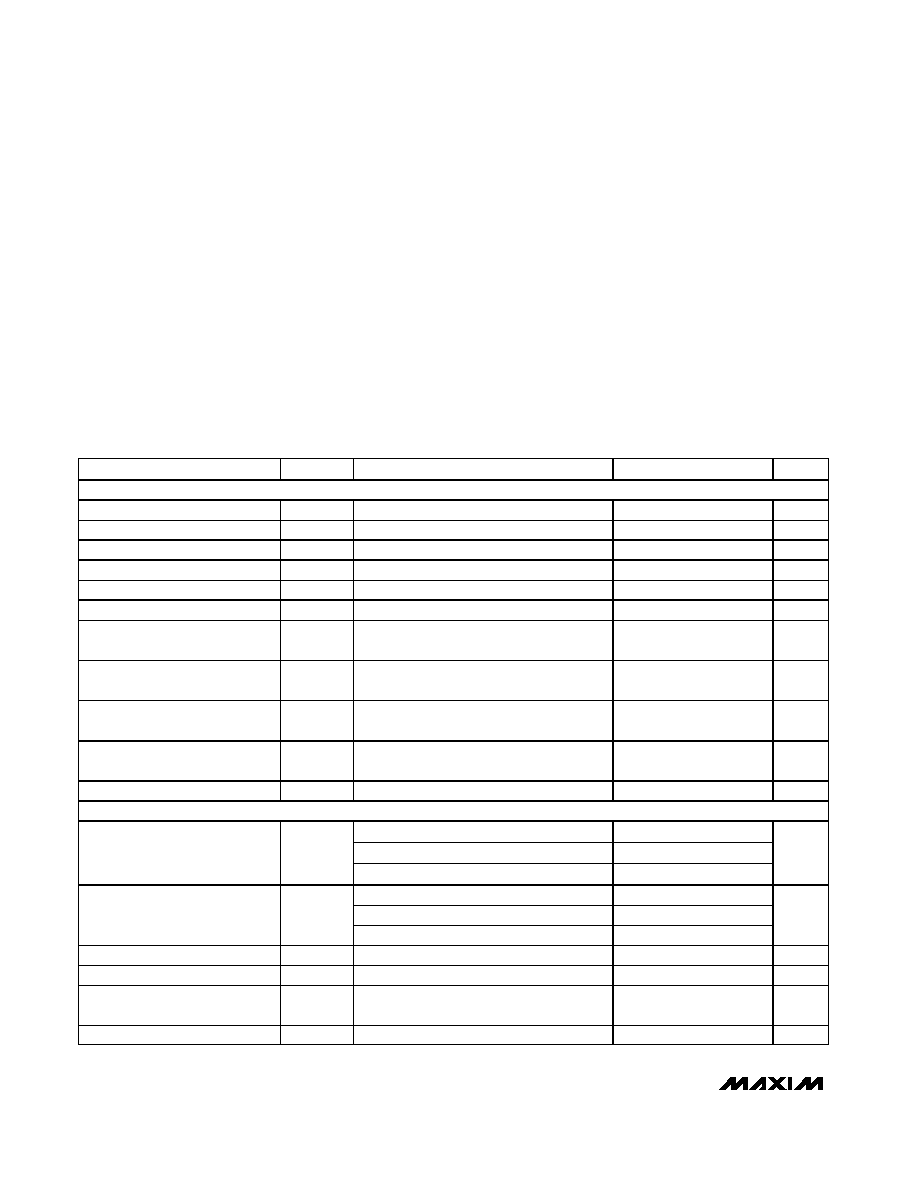
ABSOLUTE MAXIMUM RATINGS
ELECTRICAL CHARACTERISTICS
(V
DD
= +1.5V to +3.6V, V
REF
= V
DD
, C
REF
= 0.1µF, f
SCLK
= 5MHz, T
A
= T
MIN
to T
MAX
, unless otherwise noted. Typical values are at
T
A
= +25°C.)
Stresses beyond those listed under "Absolute Maximum Ratings" may cause permanent damage to the device. These are stress ratings only, and functional
operation of the device at these or any other conditions beyond those indicated in the operational sections of the specifications is not implied. Exposure to
absolute maximum rating conditions for extended periods may affect device reliability.
V
DD
to GND ..............................................................-0.3V to +4V
SCLK, CS, OE, CH1/CH2, UNI/BIP,
DOUT to GND.........................................-0.3V to (V
DD
+ 0.3V)
AIN+, AIN-, AIN1, AIN2, REF to GND ........-0.3V to (V
DD
+ 0.3V)
Maximum Current into Any Pin .........................................±50mA
Continuous Power Dissipation (T
A
= +70°C)
10-Pin TDFN (derate 18.5mW/°C above +70°C) ....1481.5mW
10-Pin µMAX (derate 5.6mW/°C above +70°C) ........444.4mW
Operating Temperature Ranges
MAX139_E_ _...................................................-40°C to +85°C
MAX139_M_ _ ................................................-55°C to +125°C
Junction Temperature ......................................................+150°C
Storage Temperature Range .............................-60°C to +150°C
Lead Temperature (soldering, 10s) .................................+300°C
PARAMETER
SYMBOL
CONDITIONS
MIN
TYP
MAX
UNITS
DC ACCURACY (Note 1)
Resolution
12
Bits
Integral Nonlinearity
INL
±1
LSB
Differential Nonlinearity
DNL
No missing code overtemperature
±1
LSB
Offset Error
0.5
±2
LSB
Gain Error
Offset nulled
0.5
±2
LSB
Total Unadjusted Error
TUE
±2
LSB
Offset-Error Temperature
Coefficient
±0.004
LSB/°C
Gain-Error Temperature
Coefficient
±0.001
LSB/°C
Channel-to-Channel Offset
Matching
MAX1396 only
±0.1
LSB
Channel-to-Channel Gain
Matching
MAX1396 only
±0.1
LSB
Input Common-Mode Rejection
CMR
V
CM
= 0 to V
DD
, MAX1393 only
±0.1
mV/V
DYNAMIC SPECIFICATIONS (Note 2)
V
REF
= V
DD
= 1.6
70
V
REF
= V
DD
= 1.82.5
69
Signal-to-Noise Plus Distortion
SINAD
V
REF
= V
DD
= 2.53.6
70
dB
V
REF
= V
DD
= 1.6
70.5
V
REF
= V
DD
= 1.82.5
70
71
Signal-to-Noise Ratio
SNR
V
REF
= V
DD
= 2.53.6
71
dB
Total Harmonic Distortion
THD
-83
-75
dBc
Spurious-Free Dynamic Range
SFDR
-85
-76
dBc
Intermodulation Distortion
IMD
f
IN1
= 73kHz at -6.5dBFS,
f
IN2
= 77kHz at -6.5dBFS
-78
dB
Channel-to-Channel Crosstalk
MAX1396 only
-70
dB
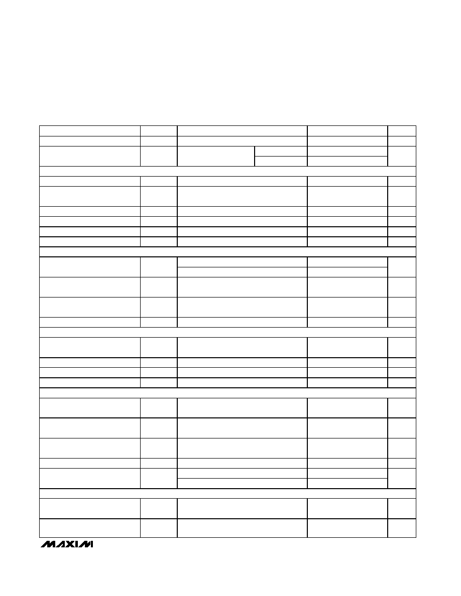
MAX1393/MAX1396
_______________________________________________________________________________________
3
1.5V to 3.6V, 312.5ksps, 1-Channel True-Differential/
2-Channel Single-Ended, 12-Bit, SAR ADCs
ELECTRICAL CHARACTERISTICS (continued)
(V
DD
= +1.5V to +3.6V, V
REF
= V
DD
, C
REF
= 0.1µF, f
SCLK
= 5MHz, T
A
= T
MIN
to T
MAX
, unless otherwise noted. Typical values are at
T
A
= +25°C.)
PARAMETER
SYMBOL
CONDITIONS
MIN
TYP
MAX
UNITS
Full-Power Bandwidth
-3dB point
4
MHz
MAX1393
200
Full-Linear Bandwidth
SINAD > 68dB
MAX1396
150
kHz
CONVERSION RATE
Conversion Time
t
CONV
13 clock cycles
2.6
µs
Throughput Rate
16 clock cycles per conversion; includes
power-up, acquisition, and conversion time
312.5
ksps
Power-Up and Acquisition Time
t
ACQ
Three SCLK cycles
600
ns
Aperture Delay
t
AD
8
ns
Aperture Jitter
t
AJ
30
ps
Serial Clock Frequency
f
CLK
0.1
5.0
MHz
ANALOG INPUTS (AIN+, AIN-, AIN1, AIN2)
Unipolar
0
V
REF
Input Voltage Range
V
IN
Bipolar, MAX1393 only, (AIN+ - AIN-)
-V
REF
/2
+V
REF
/2
V
Common-Mode Input Voltage
Range
V
CM
Bipolar, MAX1393 only, [(AIN+) + (AIN-)] / 2
0
V
DD
V
Input Leakage Current
Channel not selected, or conversion
stopped, or in shutdown mode
±1
µA
Input Capacitance
16
pF
REFERENCE INPUT (REF)
REF Input Voltage Range
V
REF
0.6
V
DD
+
0.05
V
REF Input Capacitance
24
pF
REF DC Leakage Current
0.025
±2.5
µA
REF Input Dynamic Current
312.5ksps
20
60
µA
DIGITAL INPUTS (SCLK, CS, OE, CH1/CH2, UNI/BIP)
Input-Voltage Low
V
IL
0.3 x
V
DD
V
Input-Voltage High
V
IH
0.7 x
V
DD
V
Input Hysteresis
0.06 x
V
DD
V
Input Leakage Current
I
IL
Inputs at GND or V
DD
±1
µA
CS, OE
1
Input Capacitance
C
IN
CH1/CH2, UNI/BIP
12.5
pF
DIGITAL OUTPUT (DOUT)
Output-Voltage Low
V
OL
I
SINK
= 2mA
0.1 x
V
DD
V
Output-Voltage High
V
OH
I
SOURCE
= 2mA
0.9 x
V
DD
V
MAX1393/MAX1396
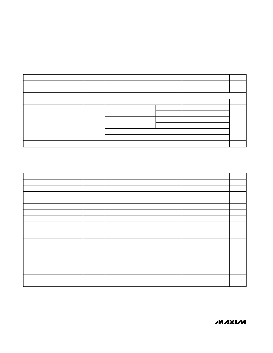
4
_______________________________________________________________________________________
1.5V to 3.6V, 312.5ksps, 1-Channel True-Differential/
2-Channel Single-Ended, 12-Bit, SAR ADCs
ELECTRICAL CHARACTERISTICS (continued)
(V
DD
= +1.5V to +3.6V, V
REF
= V
DD
, C
REF
= 0.1µF, f
SCLK
= 5MHz, T
A
= T
MIN
to T
MAX
, unless otherwise noted. Typical values are at
T
A
= +25°C.)
PARAMETER
SYMBOL
CONDITIONS
MIN
TYP
MAX
UNITS
Tri-State Leakage Current
I
LT
OE = V
DD
±1
µA
Tri-State Output Capacitance
C
OUT
OE = V
DD
10
pF
POWER SUPPLY
Positive Supply Voltage
V
DD
1.5
3.6
V
V
DD
= 1.6V
176
200
f
SAMPLE
= 100ksps
V
DD
= 3V
225
260
V
DD
= 1.6V
520
600
f
SAMPLE
= 312.5ksps
V
DD
= 3V
710
800
Power-down mode (Note 4)
5
10
Positive Supply Current (Note 3)
I
DD
Power-down mode (Note 5)
0.2
±2.5
µA
Power-Supply Rejection
PSR
V
DD
= 1.5V to 3.6V, full-scale input (Note 6)
±150
±1000
µV/V
TIMING CHARACTERISTICS
(V
DD
= +1.5V to +3.6V, V
REF
= V
DD
, C
REF
= 0.1µF, f
SCLK
= 5MHz, T
A
= T
MIN
to T
MAX
, unless otherwise noted. Typical values are at
T
A
= +25°C.) (Figure 1)
PARAMETER
SYMBOL
CONDITIONS
MIN
TYP
MAX
UNITS
SCLK Clock Period
t
CP
200
10,000
ns
SCLK Pulse-Width High
t
CH
90
ns
SCLK Pulse-Width Low
t
CL
90
ns
CS Fall to SCLK Rise Setup
t
CSS
80
ns
SCLK Rise to CS Fall Ignore
t
CSO
0
ns
SCLK Fall to DOUT Valid
t
DOV
C
LOAD
= 0 to 30pF
10
80
ns
OE Rise to DOUT Disable
t
DOD
6
20
ns
OE Fall to DOUT Enable
t
DOE
9
20
ns
CS Pulse-Width High or Low
t
CSW
80
ns
OE Pulse-Width High or Low
t
OEW
80
ns
CH1/CH2 Setup Time (to the
First SCLK)
t
CHS
MAX1396 only
10
ns
CH1/CH2 Hold Time (to the First
SCLK)
t
CHH
MAX1396 only
0
ns
UNI/BIP Setup Time (to the First
SCLK)
t
UBS
MAX1393 only
10
ns
UNI/BIP Hold Time (to the First
SCLK)
t
UBH
MAX1393 only
0
ns
Note 1: V
DD
= 1.5V, V
REF
= 1.5V, and V
AIN
= 1.5V.
Note 2: V
DD
= 1.5V, V
REF
= 1.5V, V
AIN
= 1.5V
P-P
, f
SCLK
= 5MHz, f
SAMPLE
= 312.5ksps, and f
IN
(sine wave) = 75kHz.
Note 3: All digital inputs swing between V
DD
and GND. V
REF
= V
DD
, f
IN
= 75kHz sine wave, V
AIN
= V
REFP-P,
C
LOAD
= 30pF on DOUT.
Note 4: CS = V
DD
, OE = UNI/BIP = CH1/CH2 = V
DD
or GND, SCLK is active.
Note 5: CS = V
DD
, OE = UNI/BIP = CH1/CH2 = V
DD
or GND, SCLK is inactive.
Note 6: Change in V
AIN
at code boundary 4094.5.
MAX1393/MAX1396
_______________________________________________________________________________________
5
1.5V to 3.6V, 312.5ksps, 1-Channel True-Differential/
2-Channel Single-Ended, 12-Bit, SAR ADCs
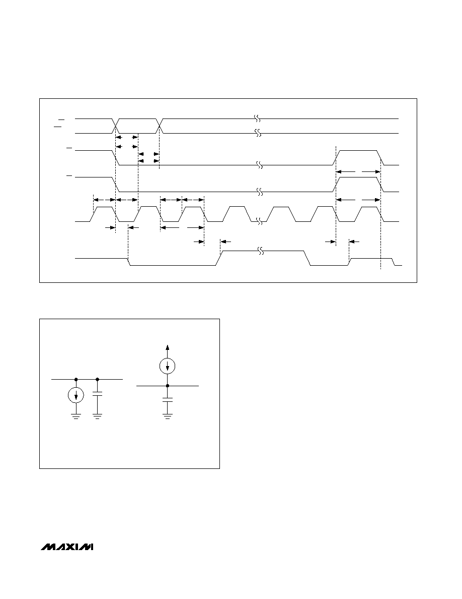
CS
SCLK
DOUT
OE
UNI/BIP OR
CH1/CH2
t
UBS
t
CHS
t
UBH
t
CHH
t
CSO
t
CSS
t
CL
t
CH
t
CP
t
DOE
HIGH-Z
t
DOV
t
OEW
t
CSW
t
DOD
HIGH-Z
Figure 1. Detailed Serial-Interface Timing Diagram
GND
50pF
50pF
DOUT
DOUT
GND
V
DD
a) HIGH IMPEDANCE TO V
OH
,
V
OL
TO V
OH
,
AND V
OH
TO HIGH IMPEDANCE
b) HIGH IMPEDANCE TO V
OL
,
V
OH
TO V
OL
,
AND V
OL
TO HIGH IMPEDANCE
10mA
10mA
Figure 2. Load Circuits for Enable/Disable Times