 | –≠–ª–µ–∫—Ç—Ä–æ–Ω–Ω—ã–π –∫–æ–º–ø–æ–Ω–µ–Ω—Ç: MAX1409 | –°–∫–∞—á–∞—Ç—å:  PDF PDF  ZIP ZIP |
General Description
The MAX1407/MAX1408/MAX1409/MAX1414 are low-
power, general-purpose, multichannel data-acquisition
systems (DAS). These devices are optimized for low-
power applications. All the devices operate from a sin-
gle +2.7V to +3.6V power supply and consume a
maximum of 1.15mA in Run mode and only 2.5µA in
Sleep mode.
The MAX1407/MAX1408/MAX1414 feature a differential
8:1 input multiplexer to the ADC, a programmable
three-state digital output, an output to shutdown an
external power supply, and a data ready output from
the ADC. The MAX1408 has eight auxiliary analog
inputs, while the MAX1407/MAX1414 include four auxil-
iary analog inputs and two 10-bit force/sense DACs.
The MAX1414 features a 50mV trip threshold for the
signal-detect comparator while the others have a 0mV
trip threshold. The MAX1409 is a 20-pin version of the
DAS family with a differential 4:1 input multiplexer to the
ADC, one auxiliary analog input, and one 10-bit
force/sense DAC.
The MAX1407/MAX1408/MAX1414 are available in
space-saving 28-pin SSOP packages, while the
MAX1409 is available in a 20-pin SSOP package.
Applications
Medical Instruments
Industrial Control Systems
Portable Equipment
Data-Acquisition System
Automatic Testing
Robotics
Features
o +2.7V to +3.6V Supply Voltage Range in Standby,
Idle, and Run Mode (Down to 1.8V in Sleep Mode)
o 1.15mA Run Mode Supply Current
o 2.5µA Sleep Mode Supply Current (Wake-Up, RTC,
and Voltage Monitor Active)
o Multichannel 16-Bit Sigma-Delta ADC
±1.5 LSB (typ) Integral Nonlinearity
30Hz or 60Hz Continuous Conversion Rate
Buffered or Unbuffered Mode
Gain of +1/3, +1, or +2V/V
Unipolar or Bipolar Mode
On-Chip Offset Calibration
o 10-Bit Force/Sense DACs
o Buffered 1.25V, 18ppm/∞C (typ) Bandgap
Reference Output
o SPITM/QSPITM or MICROWIRETM-Compatible Serial
Interface
o System Support Functions
RTC (Valid til 9999) and Alarm
High-Frequency PLL Clock Output (2.4576MHz)
+1.8V and +2.7V RESET and Power-Supply
Voltage Monitors
Signal Detect Comparator
Interrupt Generator (INT and DRDY)
Three-State Digital Output
Wake-Up Circuitry
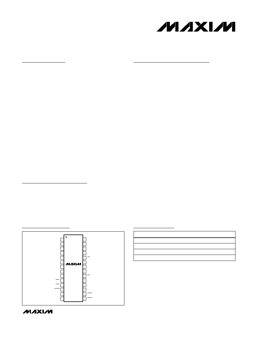
o 28-Pin SSOP (MAX1407/MAX1408/MAX1414),
20-Pin SSOP (MAX1409)
MAX1407/MAX1408/MAX1409/MAX1414
Low-Power, 16-Bit Multichannel DAS with
Internal Reference,10-Bit DACs, and RTC
________________________________________________________________ Maxim Integrated Products
1
19-2229; Rev 0; 10/01
Pin Configurations continued at end of data sheet.
Typical Operating Circuit appears at end of data sheet.
SPI and QSPI are trademarks of Motorola, Inc.
MICROWIRE is a trademark of National Semiconductor Corp.
Ordering Information
PART
TEMP. RANGE
PIN-PACKAGE
MAX1407CAI
0
∞C to +70∞C
28 SSOP
MAX1408CAI
0
∞C to +70∞C
28 SSOP
MAX1409CAP
0
∞C to +70∞C
20 SSOP
MAX1414CAI
0
∞C to +70∞C
28 SSOP
28
27
26
25
24
23
22
21
20
19
18
17
16
15
1
2
3
4
5
6
7
8
9
10
11
12
13
14
OUT2
IN3
DV
DD
DGND
SCLK
DIN
DOUT
CLKIN
CLKOUT
FOUT
IN2
IN1
CPLL
AV
DD
AGND
REF
IN0
OUT1
FB1
DO
FB2
TOP VIEW
MAX1407
MAX1414
CS
WU2
RESET
WU1
INT
DRDY
SHDN
Pin Configurations
For pricing, delivery, and ordering information, please contact Maxim/Dallas Direct! at
1-888-629-4642, or visit Maxim's website at www.maxim-ic.com.

MAX1407/MAX1408/MAX1409/MAX1414
Low-Power, 16-Bit Multichannel DAS with
Internal Reference,10-Bit DACs, and RTC
2
_______________________________________________________________________________________
ABSOLUTE MAXIMUM RATINGS
Stresses beyond those listed under "Absolute Maximum Ratings" may cause permanent damage to the device. These are stress ratings only, and functional
operation of the device at these or any other conditions beyond those indicated in the operational sections of the specifications is not implied. Exposure to
absolute maximum rating conditions for extended periods may affect device reliability.
AV
DD
to AGND .........................................................-0.3V to +6V
AV
DD
to DV
DD
...................................................... -0.3V to +0.3V
Analog Inputs to AGND .........................-0.3V to +(AV
DD
+ 0.3V)
Digital Inputs to DGND.............................................-0.3V to +6V
Maximum Current Input Into Any Pin ..................................50mA
Continuous Power Dissipation (T
A
= +70∞C)
20-Pin SSOP (derate 8.0mW/∞C above +70∞C) ...........640mW
28-Pin SSOP (derate 9.52mW/∞C above +70∞C) .........762mW
DV
DD
to DGND.........................................................-0.3V to +6V
AGND to DGND.....................................................-0.3V to +0.3V
Analog Outputs to AGND ......................-0.3V to +(AV
DD
+ 0.3V)
Digital Outputs to DGND .......................-0.3V to +(AV
DD
+ 0.3V)
REF to AGND.........................................-0.3V to +(AV
DD
+ 0.3V)
Operating Temperature Range:
MAX14__CA_ ......................................................0∞C to +70∞C
MAX14__EA_ ...................................................-40∞C to +85∞C
Lead Temperature (soldering, 10s) ................................+300 ∞C
Storage Temperature Range .............................-65∞C to +150∞C
Junction Temperature ......................................................+150∞C
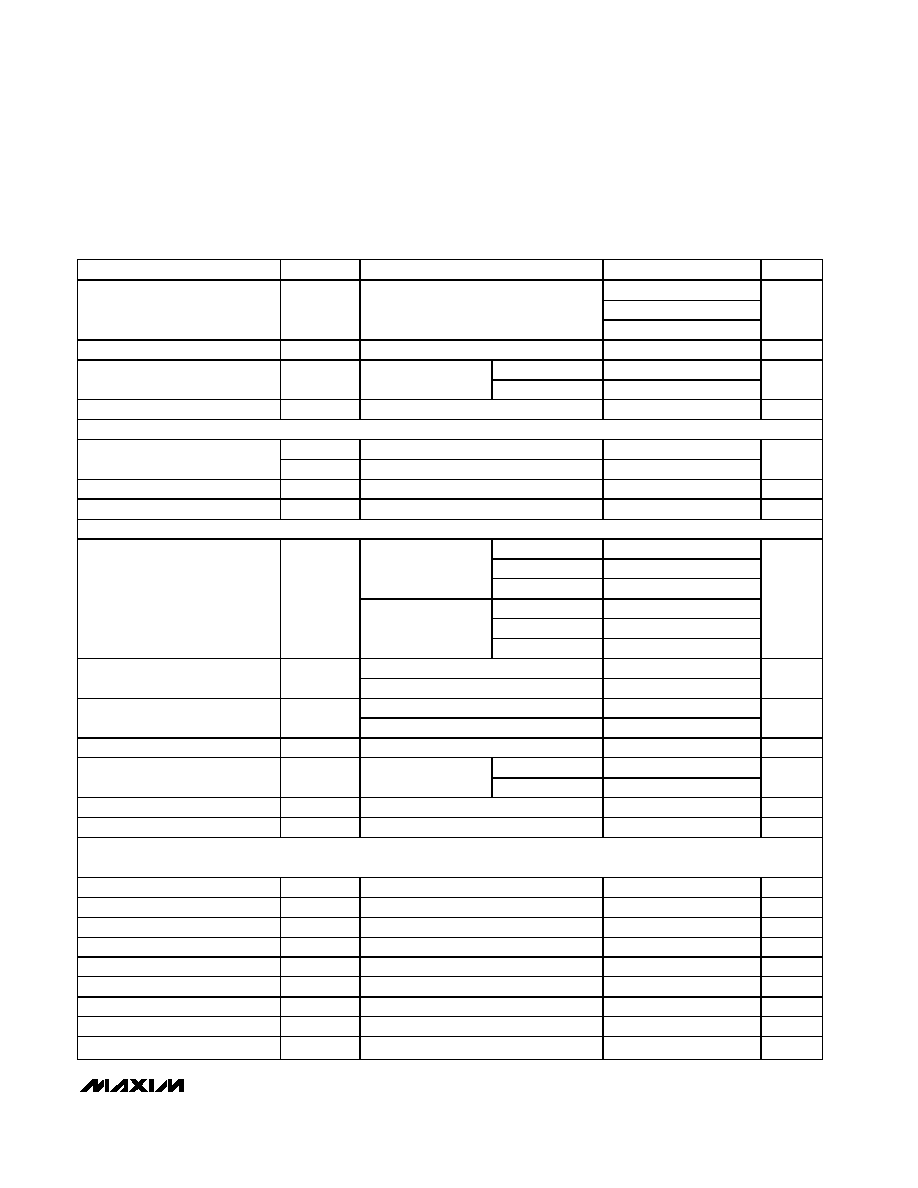
ELECTRICAL CHARACTERISTICS
(DV
DD
= AV
DD
= +2.7V to 3.6V, 4.7µF at REF, internal V
REF
, 18nF between CPLL and AV
DD
, 32.768kHz crystal across CLKIN and
CLKOUT, T
A
= T
MIN
to T
MAX
, unless otherwise noted. Typical values are at T
A
= +25∞C.)
PARAMETER
SYMBOL
CONDITIONS
MIN
TYP
MAX
U N I T S
ADC ACCURACY
Resolution (No Missing Codes)
RES
16
Bits
Unbuffered mode, Unipolar mode, gain = 1,
V
NEG
= 0.2V, fully differential input (Note 7)
1.5
3.5
U nb uffer ed m od e, U ni p ol ar m od e, g ai n = 2,
V
N E G
= 0.625V , p seud o- d i ffer enti al i np ut
1.75
Unbuffered mode, Bipolar mode, gain = 1,
V
NEG
= 0.625V, fully differential input
1.70
Integral Nonlinearity
INL
Buffered mode, Bipolar mode, gain = 2,
V
NEG
= 0.625V, fully differential input
2.50
LSB
Gain = 2
±5
Gain = 1
±10
Unipolar
Gain = 1/3
±30
Gain = 2
±8
Gain = 1
±16.5
Output RMS Noise (Note 1)
Bipolar Mode
Gain = 1/3
±48.5
µV
RMS
Offset Error
On-chip calibration removes this error
±1
% of FS R
Offset Drift
±0.5
µV/∞C
Gain Error
Excludes offset and reference errors
±1
% of FS R
Gain Drift
Excludes offset and reference errors
±1
p p m /∞ C
MAX1407/MAX1408/MAX1409/MAX1414
Low-Power, 16-Bit Multichannel DAS with
Internal Reference,10-Bit DACs, and RTC
_______________________________________________________________________________________
3
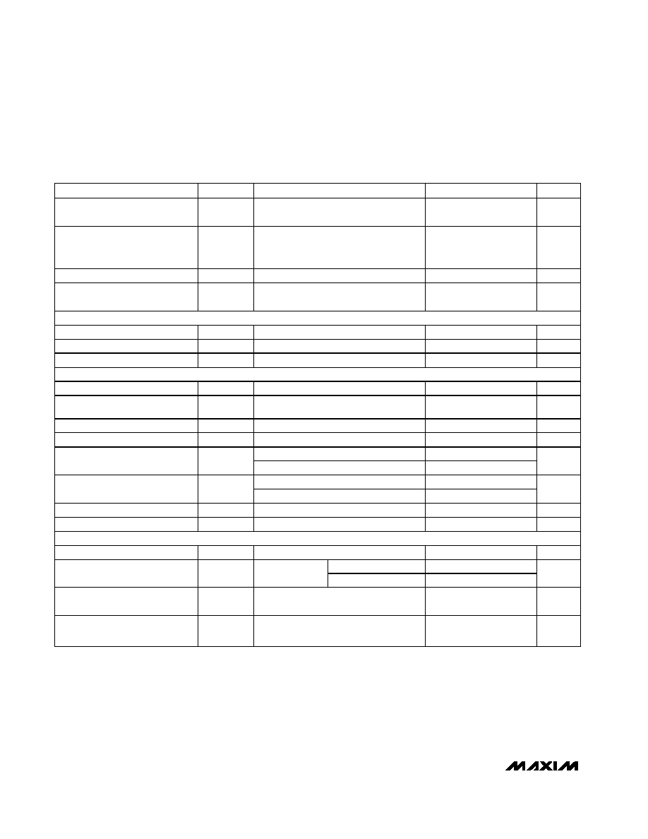
ELECTRICAL CHARACTERISTICS (continued)
(DV
DD
= AV
DD
= +2.7V to 3.6V, 4.7µF at REF, internal V
REF
, 18nF between CPLL and AV
DD
, 32.768kHz crystal across CLKIN and
CLKOUT, T
A
= T
MIN
to T
MAX
, unless otherwise noted. Typical values are at T
A
= +25∞C.)
PARAMETER
SYMBOL
CONDITIONS
MIN
TYP
MAX
U N I T S
1/3
1
PGA Gain
See PGA Gain section
2
V/V
Power-Supply Rejection Ratio
Gain = 1, unipolar and buffered mode
70
dB
RATE bit = 0
30
Output Update Rate
Continuous
conversion
RATE bit = 1
60
Hz
Turn-On Time
Excluding reference
50
µs
SIGNAL DETECT COMPARATOR
MAX1407/MAX1408/MAX1409
-10
0
10
Differential Input-Detection
Threshold Voltage
MAX1414
44
50
56
mV
Common-Mode Input Voltage
0
0.8
V
Turn-On Time
10
µs
ANALOG INPUTS
ADC gain = 1
0
V
REF
ADC gain = 2
0
V
REF/2
Unipolar mode
ADC gain = 1/3
0
AV
DD
ADC gain = 1
-V
REF
V
REF
ADC gain = 2
-V
REF/2
V
REF/2
Differential Input Voltage Range
Bipolar mode
ADC gain = 1/3
-AV
DD
AV
DD
V
Unbuffered
-0.05
AV
DD
Absolute Input Voltage Range
Buffered
0.05
1.40
V
Unbuffered
AGND
AV
DD
Common-Mode Input Voltage
Range
Buffered
0.05
1.40
V
Common-Mode Rejection Ratio
Gain = 1, unipolar and buffered mode
90
dB
30Hz data rate
15.360
Input Sampling Rate
FOUT = 2.4576MHz
60Hz data rate
30.720
kHz
Input Current
Buffered mode
±0.5
nA
Input Capacitance
15
pF
F O R C E- SEN SE D A C ( al l m easur em ents m ad e w i th FB1( 2) shor ted to O U T1( 2) , unl ess other w i se noted ) .
( M AX 1407/M AX 1409/M AX 1414 onl y)
Resolution
10
Bits
Differential Nonlinearity
Guaranteed monotonic (Note 2)
±1.0
LSB
Integral Nonlinearity
(Note 2)
±1.0
LSB
Offset Error
(Note 3)
±20
mV
Offset Drift
±5
µV/∞C
Gain Error
Excludes offset and reference drift
3.6
mV
Gain Drift
Excludes offset and reference drift
10
ppm/∞C
Line Regulation
190
µV/V
Current into FB1(2)
±0.5
nA
MAX1407/MAX1408/MAX1409/MAX1414
Low-Power, 16-Bit Multichannel DAS with
Internal Reference,10-Bit DACs, and RTC
4
_______________________________________________________________________________________
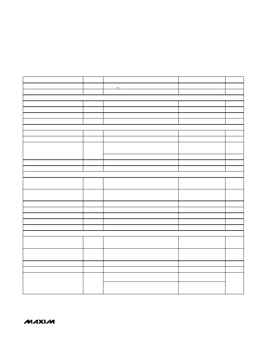
ELECTRICAL CHARACTERISTICS (continued)
(DV
DD
= AV
DD
= +2.7V to 3.6V, 4.7µF at REF, internal V
REF
, 18nF between CPLL and AV
DD
, 32.768kHz crystal across CLKIN and
CLKOUT, T
A
= T
MIN
to T
MAX
, unless otherwise noted. Typical values are at T
A
= +25∞C.)
PARAMETER
SYMBOL
CONDITIONS
MIN
TYP
MAX
U N I T S
Output Slew Rate
010hex to 3FFhex and 3FFhex to 010hex
cod e sw i ng , R
L
= 12k
, C
L
= 200p F
18.0
V/ms
Output Settling Time
To
±1/2 LSB (at 10-bit accuracy) of full-
scale with code transition from 010hex
to 3FFhex, R
L
= 12k
, C
L
= 200pF
65
µs
Turn-On Time
100
µs
OUT1, OUT2 Output Range
No Load (Note 4)
0.05
AV
DD
- 0.2
V
EXTERNAL REFERENCE (internal reference powered down)
Input Voltage Range
1.25 ±0.10
V
Input Resistance
540
k
Input Current
2.3
µA
INTERNAL REFERENCE (AV
DD
= 3V, unless otherwise noted)
Output Voltage
T
A
= +25∞C
1.225
1.25
1.275
V
Output Voltage Temperature
Coefficient
18
p p m /∞ C
Output Short-Circuit Current
3.4
mA
Line Regulation
V
RE F
/
V
DD
2.7<AV
DD
<3.6V
80
µV/V
I
SOURCE
= 0µA to 500µA, T
A
= +25∞C
1
Load Regulation
I
SINK
= 0µA to 50µA, T
A
= +25∞C
2
µV/µA
0.1Hz to 10Hz
40
Noise Voltage
e
OUT
10Hz to 10kHz
400
µVp-p
Power-Supply Rejection Ratio
±100mV, f = 120Hz
70
dB
Turn-On Time
3
ms
µP RESET
Supply Voltage Range
For valid RESET
1
3.6
V
Bit VM = 1
1.800
1.865
1.930
RESET Trip Threshold Low
V
TH
AV
DD
falling
Bit VM = 0
2.70
2.75
2.80
V
Low AV
DD
Trip Threshold
For Normal, Idle, and Standby modes,
AV
DD
falling
2.70
2.75
2.80
V
RESET Output Low Voltage
(Open-Drain Output)
I
SINK
= 1mA, AV
DD
= 1.8V
0.4
V
MAX1407/MAX1408/MAX1409/MAX1414
Low-Power, 16-Bit Multichannel DAS with
Internal Reference,10-Bit DACs, and RTC
_______________________________________________________________________________________
5
ELECTRICAL CHARACTERISTICS (continued)
(DV
DD
= AV
DD
= +2.7V to 3.6V, 4.7µF at REF, internal V
REF
, 18nF between CPLL and AV
DD
, 32.768kHz crystal across CLKIN and
CLKOUT, T
A
= T
MIN
to T
MAX
, unless otherwise noted. Typical values are at T
A
= +25∞C.)
PARAMETER
SYMBOL
CONDITIONS
MIN
TYP
MAX
U N I T S
RESET Output Leakage
AV
DD
>
V
TH
, RESET deasserted
0.002
0.1
µA
Turn-On Time
2
ms
CRYSTAL OSCILLATOR
Crystal Frequency
AV
DD
= +3V
32.768
kHz
Crystal Load Capacitance
6
pF
Oscillator Stability
AV
D D
= + 1.8V to + 3.6V , excl ud i ng cr ystal 0
ppm/V
Oscillator Startup Time
1.5
s
PLL
FOUT Frequency
AV
DD
= +3V
2.4576
MHz
Absolute Clock Jitter
Cycle-to-cycle
10
ns
Overtemperature excluding crystal,
T
A
= T
MIN
to T
MAX
0
p p m /∞ C
Frequency Tolerance/Stability
Over supp l y vol tag e, + 2.7V < AV
D D
< +3.6V
0
p p m /m V
FOUT Rise/Fall Time
20% to 80% waveform, C
L
= 30pF
15
30
ns
Duty Cycle
40
50
60
%
DIGITAL INPUTS (DIN, SCLK, CS, WU1, WU2)
Input High Voltage
DV
DD
= +1.8V to +3.6V
0.7 x
DV
DD
V
Input Low Voltage
DV
DD
= +1.8V to +3.6V
0.3 x
DV
DD
V
Input Hysteresis
DV
DD
= +3V
200
mV
DIN, SCLK, CS, Input Current
V
IN
= 0 or V
IN
= DV
DD
±0.01
±10
µA
WU1, WU2 Input Current
V
IN
= AV
DD
0.01
10
µA
WU1, WU2 Pullup Current
V
IN
= 0
10
µA
Input Capacitance
10
pF
DIGITAL OUTPUTS (DOUT, FOUT, INT, DRDY, SHDN, D0)
DOUT, FOUT, DRDY, INT
Output Low Voltage
V
OL
I
SINK
= 1mA, DV
DD
= +1.8V to +3.6V
0.4
V
DOUT, FOUT, DRDY, INT,
SHDN Output High Voltage
V
OH
I
SOURCE
= 0.2mA, DV
DD
= +1.8V to +3.6V
0.8 x DV
DD
V
DOUT Three-State Leakage
±0.01
±10
µA
DOUT Three-State Capacitance
15
pF
I
SINK
= 1mA, DV
DD
= +1.8V to +3.6V
0.4
SHDN Output Low Voltage
(MAX1407/MAX1408/MAX1414
only)
I
SINK
= 50µA, DV
DD
= +1.8V to +3.6V
0.04 x
DV
DD
V