
General Description
The MAX1415/MAX1416 low-power, 2-channel, serial-
output analog-to-digital converters (ADCs) use a sigma-
delta modulator with a digital filter to achieve 16-bit
resolution with no missing codes. These ADCs are pin-
compatible upgrades to the MX7705/AD7705. The
MAX1415/MAX1416 feature an internal oscillator (1MHz
or 2.4576MHz), an on-chip input buffer, and a program-
mable gain amplifier (PGA). The devices offer an SPITM-/
QSPITM-/MICROWIRETM-compatible serial interface.
The MAX1415 requires a single 2.7V to 3.6V supply, and
the MAX1416 requires a single 4.75V to 5.25V supply.
The operating supply current is 400µA (max) with a 3V
supply. Power-down mode reduces the supply current to
2µA (typ). When operating with a supply of 3V, the power
dissipation is less than 1.44mW, making the MAX1415
ideal for battery-powered applications.
Self-calibration and system calibration allow the
MAX1415/MAX1416 to correct for gain and offset errors.
Excellent DC performance (±0.0015% FSR INL) and low
noise (700nV in unbuffered mode) make the MAX1415/
MAX1416 ideal for measuring low-frequency signals with
a wide dynamic range. These devices accept fully differ-
ential bipolar/unipolar inputs. An internal input buffer
allows for input signals with high source impedances. An
on-chip digital filter, with a programmable cutoff and out-
put data rate, processes the output of the sigma-delta
modulator. The first notch frequency of the digital filter is
chosen to provide 150dB rejection of common-mode
50Hz or 60Hz noise and 98dB rejection of normal-mode
50Hz or 60Hz noise. A PGA and digital filtering allow sig-
nals to be directly acquired with little or no signal-condi-
tioning requirements.
The MAX1415/MAX1416 are available in 16-pin PDIP,
SO, and TSSOP packages.
Applications
Industrial Instruments
Weigh Scales
Strain-Gauge Measurements
Loop-Powered Systems
Flow and Gas Meters
Medical Instrumentation
Pressure Transducers
Thermocouple Measurements
RTD Measurements
Features
16-Bit Sigma-Delta ADCs
Two Fully Differential Input Channels
0.0015% Integral Nonlinearity with No Missing
Codes
Internal Analog Input Buffers
Programmable Gain Amplifier (PGA) from 1 to 128
Internal Oscillator (2.4576MHz or 1MHz)
Single 2.7V to 3.6V (MAX1415) or 4.75V to 5.25V
(MAX1416) Supply
Low Power
1mW max, 3V Supply
2µA (typ) Power-Down Current
SPITM-/QSPITM-/MICROWIRETM-Compatible 3-Wire
Serial Interface
Pin Compatible with MX7705/AD7705
16-Pin PDIP, SO, and TSSOP Packages
MAX1415/MAX1416
16-Bit, Low-Power, 2-Channel,
Sigma-Delta ADCs
________________________________________________________________
Maxim Integrated Products
1
16
15
14
13
12
11
10
9
1
2
3
4
5
6
7
8
SCLK
GND
V
DD
DIN
DOUT
DRDY
AIN2-
REF-
REF+
TOP VIEW
MAX1415
MAX1416
PDIP/SO/TSSOP
CLKIN
CLKOUT
AIN2+
CS
RESET
AIN1+
AIN1-
Pin Configuration
Ordering Information
19-3163; Rev 0; 1/04
For pricing, delivery, and ordering information, please contact Maxim/Dallas Direct! at
1-888-629-4642, or visit Maxim's website at www.maxim-ic.com.
EVALUATION KIT
AVAILABLE
PART
TEMP RANGE
PIN-
PACKAGE
V
DD
(V)
MAX1415
ENE*
-45∞C to +85∞C
16 PDIP
3
MAX1415EWE*
-45∞C to +85∞C
16 Wide SO
3
MAX1415EUE
-45∞C to +85∞C
16 TSSOP
3
MAX1415AENE*
-45∞C to +85∞C
16 PDIP
3
MAX1415AEWE*
-45∞C to +85∞C
16 Wide SO
3
MAX1415AEUE*
-45∞C to +85∞C
16 TSSOP
3
MAX1415CNE*
0∞C to +70∞C
16 PDIP
3
MAX1415CWE*
0∞C to +70∞C
16 Wide SO
3
MAX1415CUE*
0∞C to +70∞C
16 TSSOP
3
SPI/QSPI are trademarks of Motorola, Inc.
MICROWIRE is a trademark of National Semiconductor Corp.
*Future product--contact factory for availability.
Ordering Information continued at end of data sheet.

MAX1415/MAX1416
16-Bit, Low-Power, 2-Channel,
Sigma-Delta ADCs
2
_______________________________________________________________________________________
ABSOLUTE MAXIMUM RATINGS
ELECTRICAL CHARACTERISTICS--MAX1415
(V
DD
= 3V, GND = 0, V
REF+
= 1.225V, V
REF-
= GND, external f
CLKIN
= 2.4576MHz, CLKDIV bit = 0, C
REF+
to GND = 0.1µF, C
REF-
to
GND = 0.1µF, T
A
= T
MIN
to T
MAX
, unless otherwise noted.)
Stresses beyond those listed under "Absolute Maximum Ratings" may cause permanent damage to the device. These are stress ratings only, and functional
operation of the device at these or any other conditions beyond those indicated in the operational sections of the specifications is not implied. Exposure to
absolute maximum rating conditions for extended periods may affect device reliability.
V
DD
to GND ..............................................................-0.3V to +6V
All Other Pins to GND.................................-0.3V to (V
DD
+ 0.3V)
Maximum Current Input into Any Pin ..................................50mA
Continuous Power Dissipation (T
A
= +70
∞C)
16-Pin PDIP (derate 10.5mW/∞C above +70∞C)...........842mW
16-Pin TSSOP (derate 9.4mW/∞C above +70∞C) .........755mW
16-Pin Wide SO (derate 9.5mW/∞C above +70∞C) ......762mW
Operating Temperature Range ..........................-40∞C to +85∞C
Storage Temperature Range .............................-60∞C to +150∞C
Junction Temperature ......................................................+150∞C
Lead Temperature (soldering, 10s) .................................+300∞C
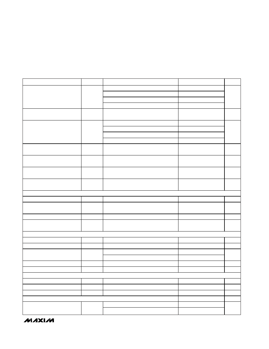
PARAMETER
SYMBOL
CONDITIONS
MIN
TYP
MAX
UNITS
DC ACCURACY
Resolution (No Missing Codes)
16
Bits
Output Noise
(Tables 1, 3)
µV
Integral Nonlinearity
INL
Gain = 1, bipolar mode, unbuffered
±
0.0015
%FSR
Unipolar Offset Error
After calibration
(Note 1)
µV
Unipolar Offset Drift
(Note 2)
0.5
µV/∞C
Bipolar Zero Error
After calibration
(Note 1)
µV
Gain = 1 to 4
0.5
Bipolar Zero Drift (Note 2)
Gain = 8 to 128
0.1
µV/∞C
Positive Full-Scale Error
After calibration
(Notes 1, 3)
µV
Full-Scale Drift
(Notes 2, 4)
0.5
µV/∞C
Gain Error
After calibration
(Notes 1, 5)
µV
Gain Drift
(Notes 2, 6)
0.5
ppm of
FSR/∞C
Bipolar Negative Full-Scale Error
After calibration
±
0.003
%FSR
Gain = 1 to 4
1
Bipolar Negative Full-Scale Drift
(Note 2)
Gain = 8 to 128
0.6
µV/∞C
ANALOG INPUTS (AIN1+, AIN1-, AIN2+, AIN2-)
Unipolar input range
0
V
REF
/
GAIN
AIN Differential Input Voltage
Range (Note 7)
Bipolar input range
-V
REF
/
GAIN
V
REF
/
GAIN
V
Unbuffered
GND -
30mV
V
DD
+
30mV
AIN Absolute Input Voltage
Range (Note 8)
Buffered
GND +
50mV
V
DD
-
1.5V
V
AIN DC Leakage Current
Unselected input channel
1
nA
MAX1415/MAX1416
16-Bit, Low-Power, 2-Channel,
Sigma-Delta ADCs
_______________________________________________________________________________________
3
ELECTRICAL CHARACTERISTICS--MAX1415 (continued)
(V
DD
= 3V, GND = 0, V
REF+
= 1.225V, V
REF-
= GND, external f
CLKIN
= 2.4576MHz, CLKDIV bit = 0, C
REF+
to GND = 0.1µF, C
REF-
to
GND = 0.1µF, T
A
= T
MIN
to T
MAX
, unless otherwise noted.)
PARAMETER
SYMBOL
CONDITIONS
MIN
TYP
MAX
UNITS
Gain = 1
34
Gain = 2
38
Gain = 4
45
AIN Input Capacitance
Gain = 8 to 128
60
pF
AIN Input Sampling Rate
f
s
Gain = 1 to 128
f
CLKIN
/
64
MHz
Gain = 1
105
Gain = 2
110
Gain = 4
120
Input Common-Mode Rejection
CMR
Gain = 8 to 128
130
dB
Normal-Mode 50Hz Rejection
For filter notches of 25Hz, 50Hz,
±0.02 ◊ f
NOTCH
98
dB
Normal-Mode 60Hz Rejection
For filter notches of 20Hz, 60Hz,
±0.02 ◊ f
NOTCH
98
dB
Common-Mode 50Hz Rejection
For filter notches of 25Hz, 50Hz,
±0.02 ◊ f
NOTCH
150
dB
Common-Mode 60Hz Rejection
For filter notches of 20Hz, 60Hz,
±0.02 ◊ f
NOTCH
150
dB
EXTERNAL REFERENCE (REF+, REF-)
REF Differential Input Range
V
REF
(Note 9)
1.00
1.75
V
REF Absolute Input Voltage
Range
GND
V
DD
V
REF Input Capacitance
Gain = 1 to 128
10
pF
REF Input Sampling Rate
f
s
f
CLKIN
/
64
MHz
DIGITAL INPUTS (DIN, SCLK,
CS
,
RESET
)
Input High Voltage
V
IH
2.0
V
Input Low Voltage
V
IL
0.4
V
DIN,
CS, RESET
250
Input Hysteresis
V
HYST
SCLK
500
mV
Input Current
I
IN
±1
µA
Input Capacitance
5
pF
CLKIN INPUT
CLKIN Input High Voltage
V
CLKINH
2.5
V
CLKIN Input Low Voltage
V
CLKINL
0.4
V
CLKIN Input Current
I
CLKIN
±10
µA
DIGITAL OUTPUTS (DOUT,
DRDY
, CLKOUT)
DOUT and
DRDY, I
SINK
= 100µA
0.4
Output-Voltage Low
V
OL
CLKOUT, I
SINK
= 10µA
0.4
V

MAX1415/MAX1416
16-Bit, Low-Power, 2-Channel,
Sigma-Delta ADCs
4
_______________________________________________________________________________________
ELECTRICAL CHARACTERISTICS--MAX1415 (continued)
(V
DD
= 3V, GND = 0, V
REF+
= 1.225V, V
REF-
= GND, external f
CLKIN
= 2.4576MHz, CLKDIV bit = 0, C
REF+
to GND = 0.1µF, C
REF-
to
GND = 0.1µF, T
A
= T
MIN
to T
MAX
, unless otherwise noted.)
PARAMETER
SYMBOL
CONDITIONS
MIN
TYP
MAX
UNITS
DOUT and
DRDY, I
SOURCE
= 100µA
V
DD
-
0.6V
Output-Voltage High
V
OH
CLKOUT, I
SOURCE
= 10µA
V
DD
-
0.6V
V
Tri-State Leakage Current
I
L
DOUT only
±10
µA
Tri-State Output Capacitance
C
OUT
DOUT only
9
pF
SYSTEM CALIBRATION
Full-Scale Calibration Range
GAIN = selected PGA gain (1 to 128)
(Note 10)
-1.05 ◊
V
REF
/
GAIN
1.05 ◊
V
REF
/
GAIN
V
Offset Calibration Range
GAIN = selected PGA gain (1 to 128)
(Note 10)
-1.05 ◊
V
REF
/
GAIN
1.05 ◊
V
REF
/
GAIN
V
Input Span
GAIN = selected PGA gain (1 to 128)
(Notes 10, 11)
0.8 ◊
V
REF
/
GAIN
2.1 ◊
V
REF
/
GAIN
V
POWER REQUIREMENTS
Power-Supply Voltage
V
DD
2.7
3.6
V
Unbuffered, f
CLKIN
= 1MHz, gain = 1 to 128
0.40
Buffered, f
CLKIN
= 1MHz, gain = 1 to 128
0.725
Gain = 1 to 4
0.55
Unbuffered,
f
CLKIN
= 2.4576MHz
Gain = 8 to 128
0.55
Gain = 1 to 4
0.825
Buffered,
f
CLKIN
= 2.4576MHz
Gain = 8 to 128
1.0
mA
Power-Supply Current (Note 12)
I
DD
Power-down mode (Note 13)
8
µA
Power-Supply Rejection Ratio
PSRR
V
DD
= 2.7V to 3.6V
(Note 14)
dB
EXTERNAL-CLOCK TIMING SPECIFICATIONS
CLKIN Frequency
f
CLKIN
(Note 15)
400
2500
kHz
Duty Cycle
40
60
%
INTERNAL-CLOCK TIMING SPECIFICATIONS
MAX1415AE__,
f
CLK
= 1MHz (CLK = 0)
or 2.4576MHz (CLK = 1)
T
A
= -40∞C to
+85∞C
±4
MAX1415C__,
f
CLK
= 1MHz (CLK = 0)
or 2.4576MHz (CLK = 1)
T
A
= 0∞C to
+70∞C
±4
T
A
= -40∞C to 0∞C
±7
Internal-Clock Frequency
f
CLK
MAX1415E__,
f
CLK
= 1MHz (CLK = 0)
or 2.4576MHz (CLK = 1)
T
A
= 0∞C to + 85∞C
±4
%

MAX1415/MAX1416
16-Bit, Low-Power, 2-Channel,
Sigma-Delta ADCs
_______________________________________________________________________________________
5
ELECTRICAL CHARACTERISTICS--MAX1415 (continued)
(V
DD
= 3V, GND = 0, V
REF+
= 1.225V, V
REF-
= GND, external f
CLKIN
= 2.4576MHz, CLKDIV bit = 0, C
REF+
to GND = 0.1µF, C
REF-
to
GND = 0.1µF, T
A
= T
MIN
to T
MAX
, unless otherwise noted.)
PARAMETER
SYMBOL
CONDITIONS
MIN
TYP
MAX
UNITS
Typical Conversion-Time
Variation
t
CONV
t
CONV
= 1/ODR
±0.5
%
ELECTRICAL CHARACTERISTICS--MAX1416
(V
DD
= 5V, GND = 0, V
REF+
= 2.5V, V
REF-
= GND, f
CLKIN
= 2.4576MHz, CLKDIV bit = 0, C
REF+
to GND = 0.1µF, C
REF-
to GND =
0.1µF, T
A
= T
MIN
to T
MAX
, unless otherwise noted.)
PARAMETER
SYMBOL
CONDITIONS
MIN
TYP
MAX
UNITS
DC ACCURACY
Resolution (No Missing Codes)
16
Bits
Output Noise
(Tables 1, 3)
µV
Integral Nonlinearity
INL
Gain = 1, bipolar mode, unbuffered
±0.0015
%FSR
Unipolar Offset Error
After calibration
(Note 1)
µV
Unipolar Offset Drift
(Note 2)
0.5
µV/∞C
Bipolar Zero Error
After calibration
(Note 1)
µV
Gain = 1 to 4
0.5
Bipolar Zero Drift (Note 2)
Gain = 8 to 128
0.1
µV/∞C
TIMING CHARACTERISTICS--MAX1415
(Note 16) (Figures 8, 9)
PARAMETER
SYMBOL
CONDITIONS
MIN
TYP
MAX
UNITS
DRDY High Time
500/
f
CLKIN
s
Reset Pulse-Width Low
100
ns
DRDY Fall to CS Fall Setup Time
t
1
0
ns
CS Fall to SCLK Rise Setup Time
t
2
120
ns
SCLK Fall to DOUT Valid Delay
t
3
0
100
ns
SCLK Pulse-Width High
t
4
100
ns
SCLK Pulse-Width Low
t
5
100
ns
CS Rise to SCLK Rise Hold Time
t
6
0
ns
Bus Relinquish Time After SCLK
Rising Edge
t
7
100
ns
SCLK Fall to
DRDY Rise Delay
t
8
100
ns
DIN to SCLK Setup Time
t
9
30
ns
DIN to SCLK Hold Time
t
10
20
ns