General Description
The MAX1447/MAX1496/MAX1498 low-power, 3.5- and
4.5-digit, analog-to-digital converters (ADCs) with inte-
grated light-emitting diode (LED) drivers operate from a
single 2.7V to 5.25V power supply. They include an
internal reference, a high-accuracy on-chip oscillator,
and a multiplexed LED display driver. An internal charge
pump generates the negative supply needed to power
the integrated input buffers for single-supply operation.
The ADC is configurable for either a Ī2V or Ī200mV
input range and it outputs its conversion results to an
LED. The MAX1496 is a 3.5-digit (Ī1999 count) device
and the MAX1447/MAX1498 are 4.5-digit (Ī19,999
count) devices.
The MAX1447/MAX1496/MAX1498 do not require exter-
nal precision integrating capacitors, autozero capaci-
tors, crystal oscillators, charge pumps, or other circuitry
required with dual-slope ADCs (commonly used in
panel meter circuits).
These devices also feature on-chip buffers for the dif-
ferential signal and reference input, allowing direct
interface with high-impedance signal sources. In addi-
tion, they use continuous internal offset-calibration and
offer >100dB rejection of 50Hz and 60Hz line noise.
Other features include data hold and peak detection
and overrange/underrange detection. The MAX1447
features on-demand enhanced offset calibration for
improved offset performance.
The MAX1447/MAX1498 are available in a 32-pin, 7mm
7mm TQFP package and the MAX1496 is available in
28-pin SSOP and 28-pin PDIP packages. All devices in
this family operate over the -40įC to +85įC extended
temperature range.
Applications
Digital Panel Meters
Hand-Held Meters
Digital Voltmeters
Digital Multimeters
Features
High Resolution
MAX1447/MAX1498: 4.5 Digits (Ī19,999 Count)
MAX1496: 3.5 Digits (Ī1999 Count)
Sigma-Delta ADC Architecture
No Integrating Capacitors Required
No Autozeroing Capacitors Required
>100dB of Simultaneous 50Hz and 60Hz
Rejection
Selectable Input Range of Ī200mV or Ī2V
Selectable Voltage Reference: Internal 2.048V or
External
Internal High-Accuracy Oscillator Needs No
External Components
Automatic Offset Calibration
On-Demand Enhanced Offset Calibration
(MAX1447)
Operate from a Single 2.7V to 5.25V Supply
Low Power (Exclude LED-Driver Current)
Maximum 744ĶA Operating Current (MAX1496)
Maximum 960ĶA Operating Current
(MAX1447/MAX1498)
Maximum 325ĶA Shutdown Current
Multiplexed Common-Cathode LED Drivers
Resistor-Programmable Segment Current
Small 32-Pin, 7mm x 7mm TQFP Package (4.5
Digits), 28-Pin SSOP Package (3.5 Digits)
Also Available in a PDIP Package (3.5 Digits)
MAX1447/MAX1496/MAX1498
3.5- and 4.5-Digit, Single-Chip ADCs
with LED Drivers
________________________________________________________________ Maxim Integrated Products
1
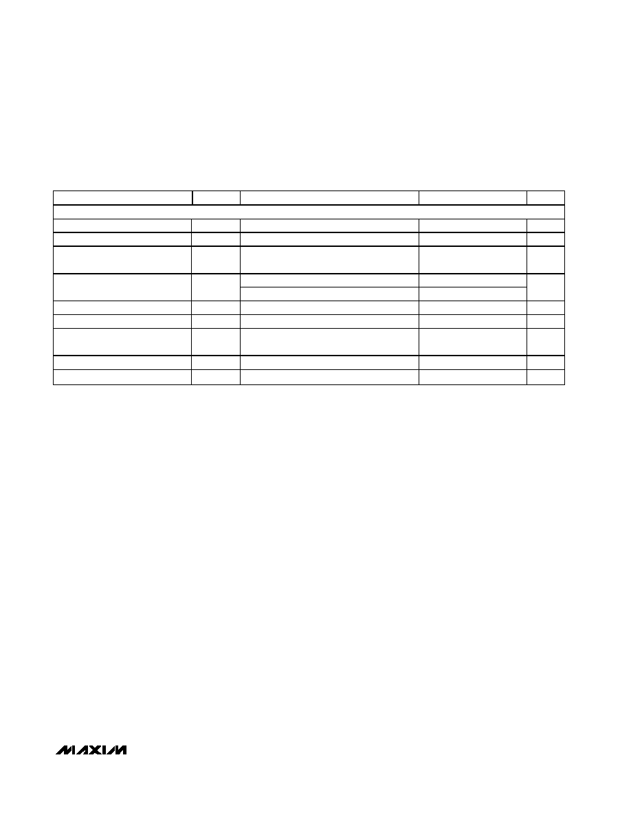
Ordering Information
19-3166; Rev 0; 1/04
For pricing, delivery, and ordering information, please contact Maxim/Dallas Direct! at
1-888-629-4642, or visit Maxim's website at www.maxim-ic.com.
PART
TEMP RANGE
PIN-
PACKAGE
RESOLUTION
(DIGITS)
MAX1447ECJ
-40
įC to +85įC 32 TQFP
4.5
MAX1496EAI*
-40
įC to +85įC 28 SSOP
3.5
MAX1496EPI
-40
įC to +85įC 28 PDIP
3.5
MAX1498ECJ
-40
įC to +85įC 32 TQFP
4.5
Pin Configurations appear at end of data sheet.
*Future product--contact factory for availability.

MAX1447/MAX1496/MAX1498
3.5- and 4.5-Digit, Single-Chip ADCs
with LED Drivers
2
_______________________________________________________________________________________
ABSOLUTE MAXIMUM RATINGS
Stresses beyond those listed under "Absolute Maximum Ratings" may cause permanent damage to the device. These are stress ratings only, and functional
operation of the device at these or any other conditions beyond those indicated in the operational sections of the specifications is not implied. Exposure to
absolute maximum rating conditions for extended periods may affect device reliability.
AV
DD
to GND (MAX1447/MAX1498) ........................-0.3V to +6V
DV
DD
to GND (MAX1447/MAX1498)........................-0.3V to +6V
AIN+, AIN- to GND
(MAX1447/MAX1498) ......................VNEG to (AV
DD
to +0.3V)
REF+, REF- to GND
(MAX1447/MAX1498) ..................... VNEG to (AV
DD
to +0.3V)
INTREF, RANGE, DPSET1, DPSET2, HOLD, PEAK,
DPON to GND (MAX1447/MAX1498) ..-0.3V to (DV
DD
+ 0.3V)
VNEG to GND (MAX1447/MAX1498).......-2.6V to (AV
DD
+ 0.3V)
LED_EN to GND (MAX1447/MAX1498) ...-0.3V to (DV
DD
+ 0.3V)
ISET to GND (MAX1447/MAX1498) .........-0.3V to (AV
DD
+ 0.3V)
V
DD
to GND (MAX1496) ...........................................-0.3V to +6V
AIN+, AIN- to GND (MAX1496)..............VNEG to (V
DD
to +0.3V)
REF+, REF- to GND (MAX1496) ........... VNEG to (V
DD
to +0.3V)
INTREF, RANGE, DPSET1, DPSET2, HOLD, PEAK,
DPON to GND (MAX1496) .....................-0.3V to (V
DD
+ 0.3V)
VNEG to GND (MAX1496)..........................-2.6V to (V
DD
+ 0.3V)
ISET to GND (MAX1496) ............................-0.3V to (V
DD
+ 0.3V)
VLED to GLED ..........................................................-0.3V to +6V
GLED to GND ........................................................-0.3V to +0.3V
SEG_ to GLED..........................................-0.3V to (VLED + 0.3V)
DIG_ to GLED ..........................................-0.3V to (VLED + 0.3V)
DIG_ Sink Current .............................................................300mA
DIG_ Source Current...........................................................50mA
SEG_ Sink Current ..............................................................50mA
SEG_ Source Current..........................................................50mA
Maximum Current Input into Any Other Pin ........................50mA
Continuous Power Dissipation (T
A
= +70įC)
32-Pin TQFP (derate 20.7mW/įC above +70įC).....1652.9mW
28-Pin SSOP (derate 9.5mW/įC above +70įC) ...........762mW
28-Pin PDIP (derate 14.3mW/įC above +70įC)......1142.9mW
Operating Temperature Range ...........................-40įC to +85įC
Junction Temperature ......................................................+150įC
Storage Temperature Range .............................-60įC to +150įC
Lead Temperature (soldering, 10s) .................................+300įC
ELECTRICAL CHARACTERISTICS
(AV
DD
= DV
DD
= V
DD
= +2.7V to +5.25V, GND = 0, V
LED
= +2.7V to +5.25V, GLED = 0, V
REF+
- V
REF-
= 2.048V (external reference),
C
REF+
= C
REF-
= 0.1ĶF, C
VNEG
= 0.1ĶF. Internal clock mode, unless otherwise noted. All specifications are at T
A
= T
MIN
to T
MAX
.
Typical values are at T
A
= +25įC, unless otherwise noted.)
PARAMETER
SYMBOL
CONDITIONS
MIN
TYP
MAX
UNITS
DC ACCURACY
MAX1447/MAX1498
-19,999
+19,999
Noise-Free Resolution
MAX1496
-1999
+1999
Counts
2.000V range
Ī1
Integral Nonlinearity (Note 1)
INL
200mV range
Ī1
Counts
Range Change Ratio
(V
AIN+
- V
AIN-
= 0.100V) on 200mV range
(V
AIN+
- V
AIN-
= 0.100V) on 2.0V range
10:1
Ratio
Rollover Error
V
AIN+
- V
AIN-
= full scale
V
AIN-
- V
AIN+
= full scale
Ī1
Counts
Output Noise
10
ĶV
P-P
Offset Error (Zero Input Reading)
Offset
V
IN
= 0 (Note 2)
-0
0
Read ings
Gain Error
(Note 3)
-0.5
+0.5
% FSR
Offset Drift (Zero Reading Drift)
V
IN
= 0 (Note 4)
0.1
ĶV/
įC
Gain Drift
Ī1
ppm/
įC
INPUT CONVERSION RATE
Conversion Rate
5
Hz

MAX1447/MAX1496/MAX1498
3.5- and 4.5-Digit, Single-Chip ADCs
with LED Drivers
_______________________________________________________________________________________
3
PARAMETER
SYMBOL
CONDITIONS
MIN
TYP
MAX
UNITS
ANALOG INPUTS (AIN+, AIN-) (bypass to GND with 0.1ĶF or greater capacitors)
RANGE = GND
-2.0
+2.0
AIN Input Voltage Range (Note 5)
RANGE = DV
DD
(MAX1447/MAX1498) or
V
DD
(MAX1496)
-0.2
+0.2
V
AIN Absolute Input Voltage
Range to GND
-2.2
+2.2
V
Normal-Mode 50Hz and 60Hz
Rejection (Simultaneously)
50Hz and 60Hz Ī2%
100
dB
Common-Mode 50Hz and 60Hz
Rejection (Simultaneously)
CMR
For 50Hz and 60Hz Ī2%, R
SOURCE
< 10k
150
dB
Common-Mode Rejection
CMR
At DC
100
dB
Input Leakage Current
10
nA
Input Capacitance
10
pF
Average Dynamic Input Current
(Note 6)
-20
+20
nA
INTERNAL REFERENCE (REF- = GND, INTREF = DV
DD
(MAX1447/MAX1498) or V
DD
(MAX1496) (bypass REF+ to GND with a
4.7ĶF capacitor)
REF Output Voltage
V
REF
2.007
2.048
2.089
V
REF Output Short-Circuit Current
1
mA
REF Output Temperature
Coefficient
TC
VREF
40
ppm/
įC
Load Regulation
I
SOURCE
= 0 to 300ĶA, I
SINK
= 0 to 30ĶA
6
mV/ĶA
Line Regulation
50
ĶV/V
0.1Hz to 10Hz
25
Noise Voltage
10Hz to 10kHz
400
ĶV
P-P
EXTERNAL REFERENCE (INTREF = GND) (bypass REF+ and REF- to GND with 0.1ĶF or greater capacitors)
REF Input Voltage
Differential, V
REF+
- V
REF-
2.048
V
Absolute REF+, REF- Input
Voltage to GND
-2.2
+2.2
V
Normal-Mode 50Hz and 60Hz
Rejection (Simultaneously)
50Hz and 60Hz Ī2%
100
dB
Common-Mode 50Hz and 60Hz
Rejection (Simultaneously)
CMR
For 50Hz and 60Hz Ī2%, R
SOURCE
< 10k
150
dB
Common-Mode Rejection
CMR
At DC
100
dB
Input Leakage Current
10
nA
Input Capacitance
10
pF
Average Dynamic Input Current
(Note 6)
-20
+20
nA
ELECTRICAL CHARACTERISTICS (continued)
(AV
DD
= DV
DD
= V
DD
= +2.7V to +5.25V, GND = 0, V
LED
= +2.7V to +5.25V, GLED = 0, V
REF+
- V
REF-
= 2.048V (external reference),
C
REF+
= C
REF-
= 0.1ĶF, C
VNEG
= 0.1ĶF. Internal clock mode, unless otherwise noted. All specifications are at T
A
= T
MIN
to T
MAX
.
Typical values are at T
A
= +25įC, unless otherwise noted.)

MAX1447/MAX1496/MAX1498
3.5- and 4.5-Digit, Single-Chip ADCs
with LED Drivers
4
_______________________________________________________________________________________
PARAMETER
SYMBOL
CONDITIONS
MIN
TYP
MAX
UNITS
CHARGE PUMP
Output Voltage
VNEG
C
VNEG
= 0.1ĶF to GND
-2.60
-2.42
-2.30
V
DIGITAL INPUTS (INTREF, RANGE, PEAK, HOLD, DPSET1, DPSET2, DPON)
Input Current
I
IN
V
IN
= 0 or DV
DD
= V
DD
-10
+10
ĶA
MAX1447/MAX1498
0.3 x
DV
DD
Input Low Voltage
V
INL
MAX1496
0.3 x
V
DD
V
MAX1447/MAX1498
0.7 x
DV
DD
Input High Voltage
V
INH
MAX1496
0.7 x
V
DD
V
Input Hysteresis
V
HYS
200
mV
POWER SUPPLY (Note 7)
V
DD
Voltage
V
DD
MAX1496
2.70
5.25
V
AV
DD
Voltage
AV
DD
MAX1447/MAX1498
2.70
5.25
V
DV
DD
Voltage
DV
DD
MAX1447/MAX1498
2.70
5.25
V
Power-Supply Rejection V
DD
PSRR
(Note 8)
80
dB
Power-Supply Rejection AV
DD
PSRR
A
(Note 8)
80
dB
Power-Supply Rejection DV
DD
PSRR
D
(Note 8)
100
dB
V
DD
= 5.25V
664
744
V
DD
= 3.3V
618
663
MAX1496 V
DD
Current (Note 9)
I
VDD
Standby mode
268
325
ĶA
AV
DD
= 5.25V
640
AV
DD
= 3.3V
600
MAX1447/MAX1498 AV
DD
Current (Note 9)
I
AVDD
Standby mode
305
ĶA
DV
DD
= 5.25V
320
DV
DD
= 3.3V
180
MAX1447/MAX1498 DV
DD
Current (Note 9)
I
DVDD
Standby mode
20
ĶA
LED Drivers Bias Current
From AV
DD
or V
DD
120
ĶA
ELECTRICAL CHARACTERISTICS (continued)
(AV
DD
= DV
DD
= V
DD
= +2.7V to +5.25V, GND = 0, V
LED
= +2.7V to +5.25V, GLED = 0, V
REF+
- V
REF-
= 2.048V (external reference),
C
REF+
= C
REF-
= 0.1ĶF, C
VNEG
= 0.1ĶF. Internal clock mode, unless otherwise noted. All specifications are at T
A
= T
MIN
to T
MAX
.
Typical values are at T
A
= +25įC, unless otherwise noted.)
MAX1447/MAX1496/MAX1498
3.5- and 4.5-Digit, Single-Chip ADCs
with LED Drivers
_______________________________________________________________________________________
5
PARAMETER
SYMBOL
CONDITIONS
MIN
TYP
MAX
UNITS
LED DRIVERS (Table 5)
LED Supply Voltage
V
LED
2.70
5.25
V
LED Shutdown Supply Current
I
SHDN
LED driver shutdown mode
10
ĶA
LED Supply Current
I
LED
Seven segments and decimal point on,
R
ISET
= 25k
176
180
mA
MAX1447/MAX1498
512
Display Scan Rate
f
OSC
MAX1496
640
Hz
Segment Current Slew Rate
I
SEG
/
t
25
mA/Ķs
DIG_ Voltage Low
V
DIG
I
DIG_
= 176mA
0.178
0.300
V
Segment Drive Source Current
Matching
I
SEG
3
Ī10
%
Segment Drive Source Current
I
SEG
V
LED
- V
SEG
= 0.6V, R
ISET
= 25k
16.0
21.5
25.5
mA
Interdigit Blanking Time
4
Ķs
ELECTRICAL CHARACTERISTICS (continued)
(AV
DD
= DV
DD
= V
DD
= +2.7V to +5.25V, GND = 0, V
LED
= +2.7V to +5.25V, GLED = 0, V
REF+
- V
REF-
= 2.048V (external reference),
C
REF+
= C
REF-
= 0.1ĶF, C
VNEG
= 0.1ĶF. Internal clock mode, unless otherwise noted. All specifications are at T
A
= T
MIN
to T
MAX
.
Typical values are at T
A
= +25įC, unless otherwise noted.)
Note 1: Integral nonlinearity is the deviation of the analog value at any code from its theoretical value after nulling the gain error and
offset error.
Note 2: Offset calibrated.
Note 3: Offset nulled.
Note 4: Drift error is eliminated by recalibration at the new temperature.
Note 5: The input voltage range for the analog inputs is given with respect to the voltage on the negative input of the differential pair.
Note 6: V
AIN
+ or V
AIN
- = -2.2V to +2.2V. V
REF
+ or V
REF
- = -2.2V to +2.2V. All input structures are identical. Production tested on
AIN+ and REF+ only.
Note 7: Power-supply currents are measured with all digital inputs at either GND or DV
DD
.
Note 8: Measured at DC by changing the power-supply voltage from 2.7V to 5.25V and measuring the effect on the conversion
error with external reference. PSRR at 50Hz and 60Hz exceeds 120dB with filter notches at 50Hz and 60Hz (Figure 2).
Note 9: LED drivers are disabled.