 | –≠–ª–µ–∫—Ç—Ä–æ–Ω–Ω—ã–π –∫–æ–º–ø–æ–Ω–µ–Ω—Ç: MAX145 | –°–∫–∞—á–∞—Ç—å:  PDF PDF  ZIP ZIP |
For free samples & the latest literature: http://www.maxim-ic.com, or phone 1-800-998-8800.
For small orders, phone 408-737-7600 ext. 3468.
________________General Description
The MAX1457 is a highly integrated analog-sensor sig-
nal processor optimized for piezoresistive sensor cali-
bration and compensation. It includes a programmable
current source for sensor excitation, a 3-bit program-
mable-gain amplifier (PGA), a 12-bit ADC, five 16-bit
DACs, and an uncommitted op amp. Achieving a total
error factor within 0.1% of the sensor's repeatability
errors, the MAX1457 compensates offset, full-span out-
put (FSO), offset TC, FSO TC, and full-span output non-
linearity of silicon piezoresistive sensors.
The MAX1457 calibrates and compensates first-order
temperature errors by adjusting the offset and span of
the input signal via digital-to-analog converters (DACs),
thereby eliminating quantization noise. If needed, resid-
ual higher-order errors are then compensated using lin-
ear interpolation of the first-order coefficients stored in
a look-up table (in external EEPROM).
The MAX1457 integrates three traditional sensor-
manufacturing operations into one automated process:
∑
Pretest: Data acquisition of sensor performance under
the control of a host test computer.
∑
Calibration and Compensation: Computation and storage
(in an external EEPROM) of calibration and compensation
coefficients determined from transducer pretest data.
∑
Final Test: Verification of transducer calibration and
compensation, without removal from a pretest socket.
Analog outputs are provided for both pressure and tem-
perature. A general-purpose, uncommitted op amp is also
included on-chip to increase the overall circuit gain, or to
facilitate the implementation of a 2-wire, 4≠20mA transmit-
ter. The serial interface is compatible with MicroWireTM
and SPITM, and directly connects to an external EEPROM.
Additionally, built-in testability features of the MAX1457
facilitate manufacturing and calibration of multiple sensor
modules, thus lowering manufacturing cost.
Although optimized for use with piezoresistive sensors,
the MAX1457 may also be used with other resistive
sensor types (i.e., accelerometers and strain gauges)
with the addition of a few external components.
_______________________Customization
Maxim can customize the MAX1457 for unique require-
ments. With a dedicated cell library of more than 90
sensor-specific functional blocks, Maxim can quickly pro-
vide customized MAX1457 solutions. Contact Maxim for
additional information.
____________________________Features
o
High Accuracy (within ±0.1% of sensor's
repeatable errors)
o
Compensates Offset, Offset TC, FSO, FSO TC,
Temperature/Pressure Nonlinearity
o
Rail-to-Rail
Æ
Analog Output for Calibrated,
Temperature-Compensated Pressure
Measurements
o
Programmable Sensor Excitation Current
o
SPI/MicroWire-Compatible Serial Interface
o
Fast Signal-Path Settling Time (<1ms)
o
Accepts Sensor Outputs from 5mV/V to 30mV/V
o
Pin-Compatible with MCA7707
MAX1457
0.1%-Accurate Signal Conditioner
for Piezoresistive Sensor Compensation
________________________________________________________________
Maxim Integrated Products
1
MAX1457
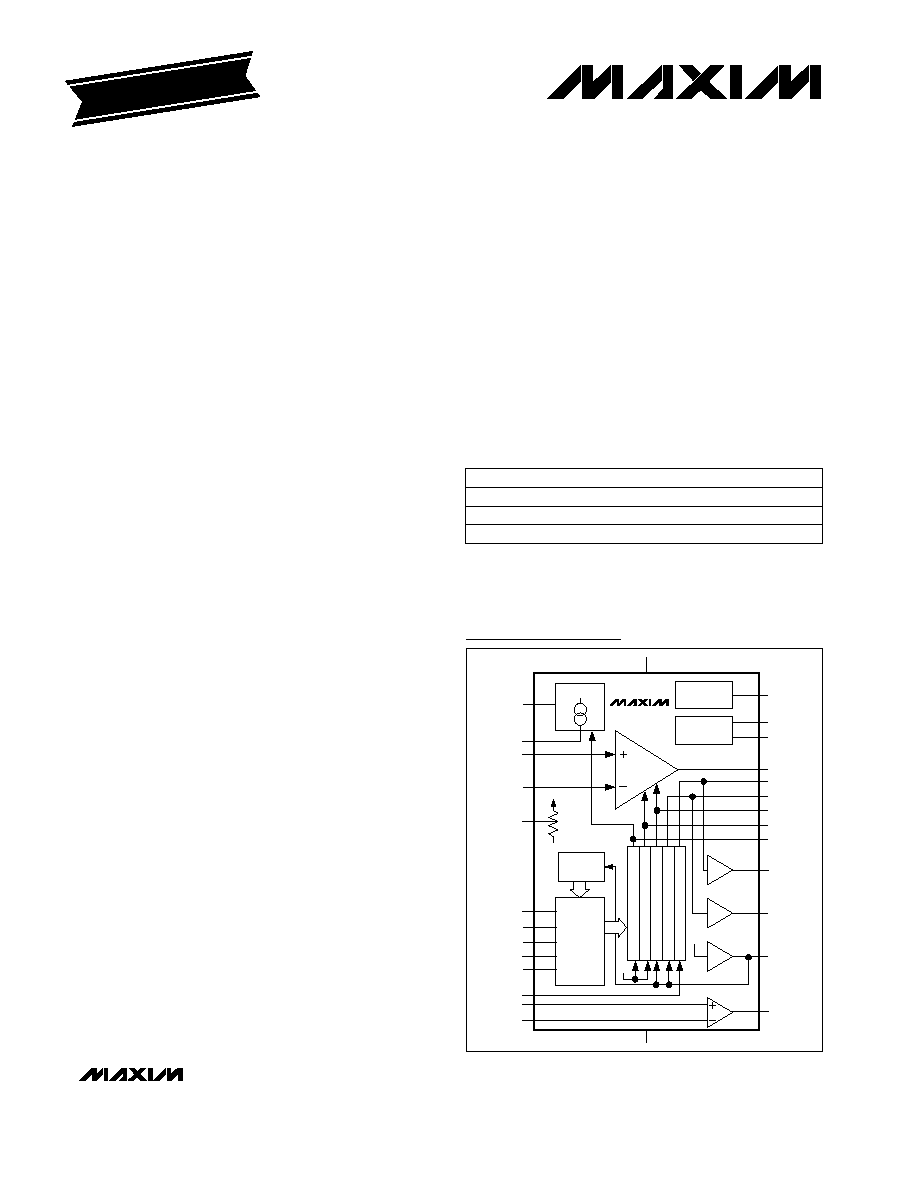
BIAS
GENERATOR
OSCILLATOR
16-BIT DAC - OFFSET TC
16-BIT DAC - OFFSET
16-BIT DAC - FSO
16-BIT DAC - FSO TC
16-BIT DAC - FSO LINEARITY
FSOTCDAC
OTCDAC
OFSTDAC
FSODAC
LINDAC
LINOUT
FSOTCOUT
VBBUF
V
BDRIVE
A = 1
A = 1
A = 1
AMPOUT
V
SS
VOUT
NBIAS
V
DD
FADJ
FOUT
SERIAL
EEPROM
INTERFACE
AGND
PGA
MCS
V
DD
ECS
ECLK
EDI
EDO
LINDACREF
AMP+
AMP-
BDRIVE
ISRC
INM
INP
V
SS
V
DD
12-BIT ADC
V
DD
19-1342; Rev 1; 8/98
PART
MAX1457CWI
MAX1457CCJ
0∞C to +70∞C
0∞C to +70∞C
TEMP. RANGE
PIN-PACKAGE
28 Wide SO
32 TQFP
EVALUATION KIT
AVAILABLE
_______________Ordering Information
Ordering Information continued at end of data sheet.
Note:
Contact the factory for customized solutions.
*
Dice are tested at T
A
= +25∞C.
Pin Configurations appear at end of data sheet.
MAX1457C/D
0∞C to +70∞C
Dice*
Rail-to-Rail is a registered trademark of Nippon Motorola, Ltd.
SPI is a trademark of Motorola, Inc.
MicroWire is a trademark of National Semiconductor Corp.
Functional Diagram
MAX1457
0.1%-Accurate Signal Conditioner
for Piezoresistive Sensor Compensation
2
_______________________________________________________________________________________
ABSOLUTE MAXIMUM RATINGS
ELECTRICAL CHARACTERISTICS
(V
DD
= +5V, V
SS
= 0V, T
A
= +25∞C, unless otherwise noted.)
Stresses beyond those listed under "Absolute Maximum Ratings" may cause permanent damage to the device. These are stress ratings only, and functional
operation of the device at these or any other conditions beyond those indicated in the operational sections of the specifications is not implied. Exposure to
absolute maximum rating conditions for extended periods may affect device reliability.
Supply Voltage, V
DD
to V
SS
......................................-0.3V to +6V
All other pins ....................................(V
SS
- 0.3V) to (V
DD
+ 0.3V)
Continuous Power Dissipation (T
A
= +70∞C)
28-Pin Wide SO (derate 12.50mW/∞C above +70∞C) ..........1W
32-Pin TQFP (derate 11.1mW/∞C above +70∞C)...........889mW
Operating Temperature Ranges
MAX1457C_ _ ......................................................0∞C to +70∞C
MAX1457A_ _ .................................................-40∞C to +125∞C
Storage Temperature Range .............................-65∞C to +150∞C
Lead Temperature (soldering, 10sec) .............................+300∞C
Reference voltage = 5.000V
R
BIAS
= 400k
, f
CLK
= 100kHz (Note 1)
Gain = 54, DC to 10Hz, sensor impedance =
5k
, full-span output = 4V
V
OUT
= (V
SS
+ 0.25V) to (V
DD
- 0.25V)
(Note 5)
(Note 4)
5k
load to V
SS
or V
DD
From V
SS
to V
DD
f
CLK
= 100kHz, to 63% of final value
(Notes 2, 3)
CONDITIONS
µV
200
DAC Voltage Resolution
V
V
SS
+ 1.3
V
DD
- 1.3
V
ISRC
Current-Source Reference Input
Voltage Range
V
V
SS
+ 1.3
V
DD
- 1.3
V
BR
Bridge Voltage Swing
mA
0.1
0.5
2.0
I
BR
Bridge Current Range
%FSO
0.0025
Output Noise
mA
-1.0
1.0
(sink) (source)
Output Current Range
V
V
SS
+ 0.02
V
DD
- 0.02
Output Voltage Swing
ppm/∞C
±50
Differential Signal Gain Tempco
V/V
54 to 306
Differential Signal Gain Range
mA
2.0
2.6
I
DD
Supply Current
V
4.5
5
5.5
V
DD
Supply Voltage
mV/V
5 to 30
Input-Referred Adjustable
Full-Span Output Range
mV
±100
Input-Referred Adjustable
Offset Range
dB
90
CMRR
Common-Mode Rejection Ratio
ms
1
Output Step-Response Time
M
1
M
1
R
IN
Input Impedance
µV/∞C
±0.5
Input-Referred Offset Tempco
%V
DD
0.01
Amplifier Gain Nonlinearity
UNITS
MIN
TYP
MAX
SYMBOL
PARAMETER
Output filter capacitor = 0.1µF, f
CLK
= 100kHz
LSB
2
Differential Nonlinearity
Bits
16
DAC Resolution
V
SS
+ 0.25
V
DD
- 0.25
T
A
= T
MIN
to T
MAX
V/V
49
54
60
Minimum Differential Signal Gain
GENERAL CHARACTERISTICS
ANALOG INPUT (PGA)
ANALOG OUTPUT (PGA)
DIGITAL-TO-ANALOG CONVERTERS
CURRENT SOURCE
No load
MAX1457
0.1%-Accurate Signal Conditioner
for Piezoresistive Sensor Compensation
_______________________________________________________________________________________
3
Note 1:
Circuit of Figure 5 with current source turned off. This value is adjustable through a bias resistor and represents the IC cur-
rent consumption. This excludes the 93C66 EEPROM average current, which is approximately 13µA at a refresh rate of 3Hz
(f
CLK
= 100kHz).
Note 2:
Temperature errors for the entire range are compensated together with the sensor errors.
Note 3:
The sensor and the MAX1457 must always be at the same temperature during calibration and use.
Note 4:
This is the maximum allowable sensor offset at minimum gain (54V/V).
Note 5:
This is the sensor's sensitivity normalized to its drive voltage, assuming a desired full-span output of 4V and a bridge volt-
age of 2.5V. Lower sensitivities can be accommodated by using the auxiliary op amp. Higher sensitivities can be accommo-
dated by operating at lower bridge voltages.
ELECTRICAL CHARACTERISTICS (continued)
(V
DD
= +5V, V
SS
= 0V, T
A
= +25∞C, unless otherwise noted.)
V
BR
= 2.5V to 3.5V, f
CLK
= 100kHz
V
OUT
= (V
SS
+ 0.25V) to (V
DD
- 0.25V)
(V
IN
- V
OUT
) at V
IN
= 2.5V,
R
BIAS
= 400k
(no load)
5k
load to V
SS
or V
DD
R
BIAS
= 400k
, V
IN
= 2.5V (no load)
R
BIAS
= 400k
, V
IN
= 2.5V,
V
OUT
= 2.5V ±20mV
f
CLK
= 100kHz
R
BIAS
= 400k
R
BIAS
= 400k
(no load)
CONDITIONS
mA
-1.0
1.0
(sink) (source)
Output Current Range
V
V
SS
+ 0.02 V
DD
- 0.02
Output Voltage Swing
mV
-20
20
Offset Voltage (as unity-gain
follower)
dB
60
A
V
Open-Loop Gain
V
V
SS
+ 1.3
V
DD
- 1.2
CMR
Input Common-Mode
Voltage Range
LSB
2
ADC Differential Nonlinearity
mV
-20
20
V
OFS
Offset Voltage
µA
-50
50
Current Drive
ms
160
Conversion Time
Bits
12
ADC Resolution
V
V
SS
+ 1.3
V
DD
- 1.3
Voltage Swing
UNITS
MIN
TYP
MAX
SYMBOL
PARAMETER
V
SS
+ 0.25 V
DD
- 0.25
ANALOG-TO-DIGITAL CONVERTER
UNCOMMITTED OP AMP
OUTPUTS
(LINDAC, FSOTCDAC)
No load

MAX1457
0.1%-Accurate Signal Conditioner
for Piezoresistive Sensor Compensation
4
_______________________________________________________________________________________
______________________________________________________________Pin Description
1
28
Positive Sensor Input. Input impedance >1M
.
Rail-to-rail input range.
2
29
Negative Sensor Input. Input impedance >1M
.
Rail-to-rail input range.
3
30
Positive Input of General-Purpose Operational Amplifier
4
31
Negative Input of General-Purpose Operational Amplifier
--
4, 16,
22, 32
Not internally connected.
7
3
PGA Output Voltage. Connect a 0.1µF capacitor from VOUT to V
SS
. High impedance when
MCS is low.
6
2
Sensor Excitation Current. This pin drives a nominal 0.5mA through the sensor.
5
1
Output of General-Purpose Operational Amplifier. High impedance when MCS is low.
12
9
Reference Input to FSO Linearity DAC. Normally tied to VOUT.
11
8
Buffered FSO Linearity DAC Output. Use a resistor (R
LIN
) greater than 100k
, from LINOUT
to ISRC to correct second order FSO nonlinearity errors. Leave unconnected if not
correcting second order FSO nonlinearity errors.
10
7
Buffered Bridge Voltage (the voltage at BDRIVE). Leave unconnected if unused.
9
6
Buffered FSO TC DAC Output. Tie to ISRC with a resistor (R
STC
50k
).
8
5
Current-Source Reference. Connect a 50k
resistor from ISRC to V
SS
.
INP
INM
AMP+
AMP-
N.C.
VOUT
BDRIVE
AMPOUT
LINDACREF
LINOUT
VBBUF
FSOTCOUT
ISRC
13
10
FSO Linearity DAC Output Voltage. Connect 0.1µF capacitor from LINDAC to V
SS
.
LINDAC
14
11
Negative Power Supply Input
V
SS
15
12
OFFSET TC DAC Output Voltage. Connect a 0.1µF capacitor from OTCDAC to V
SS
.
OTCDAC
16
13
FSO DAC Output Voltage. Connect a 0.1µF capacitor from FSODAC to V
SS
.
FSODAC
17
14
FSO TC DAC Output Voltage. Connect a 0.1µF capacitor from FSOTCDAC to V
SS
.
FSOTCDAC
18
15
OFFSET DAC Output Voltage. Connect a 0.1µF capacitor from OFSTDAC to V
SS
.
OFSTDAC
19
17
Serial Input (data from EEPROM), active high. CMOS logic-level input pin through which the
MAX1457's internal registers are updated with EEPROM coefficients. Disabled when MCS is
low.
EDO
20
18
Serial Output (data to EEPROM), active high. CMOS logic-level output pin through which
the MAX1457 gives external commands to the EEPROM. Temperature-compensation data
is available through this pin. Becomes high impedance when MCS is low.
EDI
21
19
CMOS Logic-Level Clock Output for external EEPROM. High impedance when MCS is low.
ECLK
22
20
Chip-Select Output for external EEPROM. CMOS logic-level output pin through which the
MAX1457 enables/disables EEPROM operation. High impedance when MCS is low.
ECS
23
21
Frequency Output. Internal oscillator output signal. Normally left open.
FOUT
24
23
Frequency Adjust. Connect to V
SS
with a 1.5M
resistor (R
OSC
) to set internal oscillator fre-
quency to 100kHz. Connect a 0.1µF bypass capacitor from FADJ to V
SS
.
FADJ
PIN
FUNCTION
NAME
25
24
Master Chip Select. The MAX1457 is selected when MCS is high. Leave unconnected for
normal operation (internally pulled up to V
DD
with 1M
resistor). External 5k
pull-up may
be required in noisy environments.
MCS
26
25
Bias Setting Pin. Connect to V
DD
with a 400k
resistor (R
BIAS
). Connect a 0.1µF bypass
capacitor from NBIAS to V
SS
.
NBIAS
27
26
Mid-Supply Reference for Analog Circuitry. Connect a 0.1µF capacitor from V
SS
to AGND.
AGND
28
27
Positive Power-Supply Input. Connect a 0.1µF capacitor from V
DD
to V
SS
.
V
DD
TQFP
SO
MAX1457
0.1%-Accurate Signal Conditioner
for Piezoresistive Sensor Compensation
_______________________________________________________________________________________
5
_______________Detailed Description
The MAX1457 provides an analog amplification path for
the sensor signal and a digital path for calibration and
temperature correction. Calibration and correction are
achieved by varying the offset and gain of a program-
mable-gain amplifier (PGA) and by varying the sensor
bridge current. The PGA utilizes a switched-capacitor
CMOS technology, with an input-referred offset trim-
ming range of ±100mV (20mV/V) and an approximate
3µV (input referred, at minimum gain of 54V/V) resolu-
tion (16 bits). The PGA provides eight gain values from
54V/V to 306V/V. The bridge current source is program-
mable from 0.1mA to 2mA, with a 15nA step size.
The MAX1457 uses five 16-bit DACs with calibration
coefficients stored in a low-cost external EEPROM. This
memory (an external 4096-bit EEPROM) contains the
following calibration coefficients as 16-bit words:
∑
FSO (full-span output)
∑
FSO TC (including nonlinearities)
∑
Offset
∑
Offset TC (including nonlinearities)
∑
Pressure nonlinearity
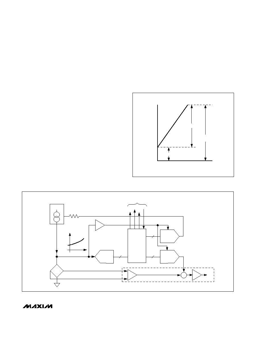
Figure 1 shows a typical pressure-sensor output and
defines the offset, full-scale, and full-span output values
as a function of voltage.
Offset Correction
Initial offset calibration is accomplished by reading a
16-bit word (coefficient) from the EEPROM and writing it
to the OFFSET DAC. The resulting voltage (OFSTDAC)
is fed into a summing junction at the PGA output for
compensating the sensor offset with a resolution of
±0.2mV (±0.005% FSO).
VOLTAGE
PRESSURE
FULL-SCALE (FS)
FULL-SPAN OUTPUT (FSO)
OFFSET
Figure 1. Typical Pressure-Sensor Output
V
BR
T
V
BR
I
BR
R
STC
V
DD
EDI
ECS
ECLK
TO/FROM
EXTERNAL EEPROM
EDO
EEPROM
INTERFACE
ADC
BDRIVE
12
16
OUTPUT
PGA
TEMPERATURE-
DEPENDENT VOLTAGE
OFFSET TC
DAC REFERENCE VOLTAGE
FSO TC
DAC
16
A = 1
Figure 2. Simplified Diagram of Temperature Error Correction