 | ÐлекÑÑоннÑй компоненÑ: MAX1462 | СкаÑаÑÑ:  PDF PDF  ZIP ZIP |
Äîêóìåíòàöèÿ è îïèñàíèÿ www.docs.chipfind.ru
General Description
The MAX1462 implements a revolutionary concept in
signal conditioning, where the output of its 16-bit ana-
log-to-digital converter (ADC) is digitally corrected over
the specified temperature range. This feature can be
readily exploited by automotive, industrial, and medical
market segments, in applications such as sensors and
smart batteries. Digital correction is provided by an
internal digital signal processor (DSP) and on-chip 128-
bit EEPROM containing user-programmed calibration
coefficients. The conditioned output is available as a
12-bit digital word and as a ratiometric (proportional to
the supply voltage) analog voltage using an on-board
12-bit digital-to-analog converter (DAC). The uncommit-
ted op amp can be used to filter the analog output.
The analog front end includes a 2-bit programmable-
gain amplifier (PGA) and a 3-bit coarse-offset (CO)
DAC, which condition the sensor's output. This coarsely
corrected signal is digitized by a 16-bit ADC. The DSP
uses the digitized sensor signal, the temperature sen-
sor, and correction coefficients stored in the internal
EEPROM to produce the conditioned output.
Multiple or batch manufacturing of sensors is support-
ed with a completely digital test interface. Built-in testa-
bility features on the MAX1462 result in the integration
of three traditional sensor-manufacturing operations
into one automated process:
· Pretest: Data acquisition of sensor performance
under the control of a host test computer.
· Calibration and compensation: Computation and
storage of calibration and compensation coefficients
determined from transducer pretest data.
· Final test operation: Verification of transducer cali-
bration and compensation, without removal from the
pretest socket.
The MAX1462 evaluation kit (EV kit) allows fast evalua-
tion and prototyping, using a piezoresistive transducer
(PRT) and a Windows
®
-based PC. The user-friendly EV
kit simplifies small-volume prototyping; it is not necessary
to understand fully the test-system interface, the calibra-
tion algorithm, or many other details to evaluate the
MAX1462 with a particular sensor. Plug the PRT into the
EV kit, plug the EV kit into a PC parallel port, connect the
sensor to an excitation source (such as a pressure con-
troller), and run the MAX1462 EV kit software. An oven is
required for thermal compensation.
Features
o Low-Voltage Operation (2.4V to 3.6V)
o Low-Noise, 310µA Single-Chip Sensor Signal
Conditioning
o High-Precision Front End Resolves <400nV of
Differential Input Signal
o On-Chip DSP and EEPROM Provide Digital
Correction of Sensor Errors
o 16-Bit Signal Path Compensates Sensor Offset
and Sensitivity and Associated Temperature
Coefficients
o 12-Bit Parallel Digital Output
o Analog Output
o Compensates a Wide Range of Sensor Sensitivity
and Offset
o Single-Shot Automated Compensation
Algorithm--No Iteration Required
o Built-In Temperature Sensor
o Three-State, 5-Wire Serial Interface Supports
High-Volume Manufacturing
________________________Applications
Hand-Held Instruments
Piezoresistive Pressure and Acceleration
Transducers and Transmitters
Industrial Pressure Sensors and Calibrators
Smart Battery Charge Systems
Weigh Scales and Strain-Gauge Measurement
Flow Meters
Dive Computers and Liquid-Level Sensing
Hydraulic Systems
Automotive Systems
Customization
Maxim can customize the MAX1462 for unique require-
ments. With a dedicated cell library of more than 90 sen-
sor-specific functional blocks, Maxim can quickly provide
customized MAX1462 solutions, including customized
microcode for unusual sensor characteristics and 2.2V
operation. Contact Maxim for further information.
MAX1462
Low-Voltage, Low-Power,
16-Bit Smart ADC
________________________________________________________________ Maxim Integrated Products
1
19-1813; Rev 0; 10/00
PART
MAX1462CCM
0°C to +70°C
TEMP. RANGE
PIN-PACKAGE
48 TQFP
Ordering Information
Functional Diagram appears at end of data sheet.
Pin Configuration appears at end of data sheet.
Windows is a registered trademark of Microsoft Corp.
EVALUATION KIT
AVAILABLE
For free samples and the latest literature, visit www.maxim-ic.com or phone 1-800-998-8800.
For small orders, phone 1-800-835-8769.
PGA Gain
MAX1462
Low-Voltage, Low-Power,
16-Bit Smart ADC
2
_______________________________________________________________________________________
ABSOLUTE MAXIMUM RATINGS
ELECTRICAL CHARACTERISTICS
(V
DD
= +2.4V to 3.6V, V
SS
= 0, f
XIN
= 2MHz, T
A
= T
MIN
to T
MAX
, unless otherwise noted.)
Stresses beyond those listed under "Absolute Maximum Ratings" may cause permanent damage to the device. These are stress ratings only, and functional
operation of the device at these or any other conditions beyond those indicated in the operational sections of the specifications is not implied. Exposure to
absolute maximum rating conditions for extended periods may affect device reliability.
Supply Voltage, V
DD
to V
SS
......................................-0.3V to +6V
All Other Pins ...................................(V
SS
- 0.3V) to (V
DD
+ 0.3V)
Short-Circuit Duration, All Outputs .............................Continuous
Continuous Power Dissipation (T
A
= +70°C)
48-Pin TQFP (derate 12.5mW/°C above +70°C )......1000mW
Operating Temperature Range...............................0°C to +70°C
Storage Temperature Range .............................-65°C to +150°C
Lead Temperature (soldering, 10s) .................................+300°C
CO-DAC code = 011
CO-DAC code = 010
Continuous conversion
CO-DAC code = 001
CO-DAC code = 000
During operation
CO-DAC code = 100
CO-DAC code = 101
CO-DAC code = 110
CO-DAC code = 111
PGA gain code = 11
PGA gain code = 10
From V
SS
to V
DD
PGA gain code = 01
PGA gain code = 00
CONDITIONS
134
149
164
81
96
111
32
47
62
-20
-5
10
-10
5
20
-62
-47
-32
-111
-96
-81
% V
DD
-164
-149
-134
Coarse Offset
90
93
96
74
77
80
59
61
64
V/V
43
46
49
µA
310
500
I
DD
Supply Current (Note 2)
V
2.4
2.7
3.6
V
DD
Supply Voltage (Note 1)
dB
90
CMRR
Common-Mode Rejection Ratio
nV/°C
±700
Input-Referred Offset TC
Hz
15
Throughput Rate
M
1.0
R
IN
Input Impedance
ppm/°C
±40
Gain Temperature Coefficient (TC)
UNITS
MIN
TYP
MAX
SYMBOL
PARAMETER
T
A
= 0°C to +70°C
5k
input impedance
PGA gain code = 00, CO-DAC code = 000
°C
1.3
Linearity
LSB/°C
260
Resolution
LSB
RMS
3
Output-Referred Noise
nV
RMS
1700
Input-Referred Noise
%
0.006
INL
Integral Nonlinearity (Note 5)
Bits
16
Resolution
ADC (Notes 3, 4)
TEMPERATURE SENSOR (Note 6)
GENERAL CHARACTERISTICS
ANALOG INPUT
PGA AND COARSE-OFFSET DAC (Notes 3, 4)
PGA Gain
MAX1462
Low-Voltage, Low-Power,
16-Bit Smart ADC
_______________________________________________________________________________________
3
CONDITIONS
UNITS
MIN
TYP
MAX
SYMBOL
PARAMETER
DAC Resolution
12
Bits
Integral Nonlinearity
INL
1
LSB
Differential Nonlinearity
DNL
0.5
LSB
Op Amp Supply Current
80
µA
Input Common-Mode Range
CMR
V
SS
+ 1.3
V
DD
- 0.9
V
Open-Loop Gain
A
V
60
dB
Offset Voltage (as Unity-Gain
Follower)
V
OS
V
IN
= max [(V
SS
+ 2.3), (V
DD
- V
SS
) / 2]
(no load)
-30
30
mV
Output Voltage Swing
No load
V
SS
+ 0.05
V
DD
- 0.05
V
Output Current Range
V
OUT
= (V
SS
+ 0.2V) to (V
DD
- 0.2V)
±200
µA
Note 1: EEPROM programming requires a minimum V
DD
= 4.75V. I
DD
may exceed its limits during this time.
Note 2: This value does not include the sensor or load current. This value does include the uncommitted op amp current. Note that
the MAX1462 will convert continuously if REPEAT MODE is set in the EEPROM.
Note 3: See the Analog Front End, Including PGA, CO-DAC, ADC, and Temperature Sensor section.
Note 4: The signal input to the ADC is the output of the PGA plus the output of the CO-DAC. The reference to the ADC is V
DD
. The
plus full-scale input to the ADC is +V
DD
and the minus full-scale input to the ADC is -V
DD
. This specification shows the con-
tribution of the CO-DAC to the ADC input.
Note 5: See Figure 2 for ADC outputs between ±85%.
Note 6: The sensor and the MAX1462 must always be at the same temperature during calibration and use.
Note 7: The Output DAC is specified using the external lowpass filter (Figure 8).
Note 8: SDIO is an input/output digital pin. It is only enabled as a digital output pin when the MAX1462 receives from the test sys-
tem the commands 8 hex or A hex (Table 4).
Note 9: XIN is a digital input pin only when the TEST pin is high.
Note 10: Guaranteed by design. Not subject to production testing.
ELECTRICAL CHARACTERISTICS (continued)
(V
DD
= +2.4V to 3.6V, V
SS
= 0, f
XIN
= 2MHz, T
A
= T
MIN
to T
MAX
, unless otherwise noted.)
Input High Voltage
V
IH
80
% V
DD
Input Low Voltage
V
IL
20
% V
DD
Input Hysteresis
V
HYST
1.0
V
Input Leakage
I
IN
V
IN
= 0 or V
DD
±10
µA
Input Capacitance
C
IN
(Note 10)
50.0
pF
Output Voltage Low
V
OL
I
SINK
= 200µA
80
% V
DD
Output Voltage High
V
OH
I
SOURCE
= 200µA
20
% V
DD
Three-State Leakage Current
I
L
CS_ = V
SS
±10
µA
Three-State Output Capacitance
C
OUT
CS_ = V
SS
(Note 10)
50.0
pF
Output Voltage Low
V
OL
I
SINK
= 200µA
10
% V
DD
Output Voltage High
V
OH
I
SOURCE
= 200µA
90
% V
DD
Three-State Leakage Current
I
L
CS_ = V
SS
±10
µA
Three-State Output Capacitance
C
OUT
CS_ = V
SS
(Note 10)
50.0
pF
OUTPUT DAC (Note 7)
UNCOMMITTED OP AMP
DIGITAL INPUTS: START, CS1, CS2, SDIO (Note 8), RESET, XIN (Note 9), TEST
DIGITAL OUTPUTS: D[11...0]
DIGITAL OUTPUTS: SDIO (Note 8), SDO, EOC, OUT
MAX1462
Low-Voltage, Low-Power,
16-Bit Smart ADC
4
_______________________________________________________________________________________
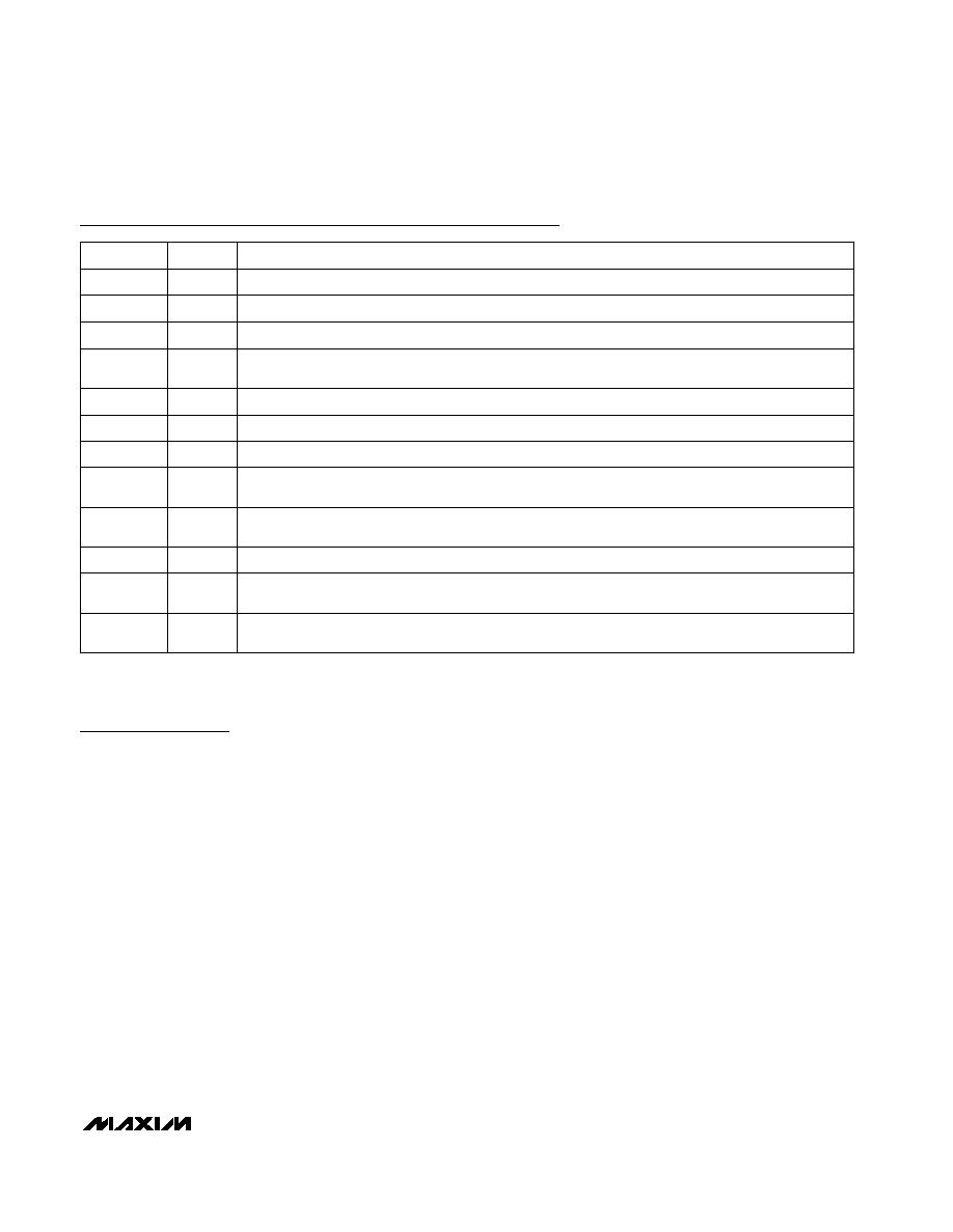
Pin Description
End of Conversion Output. A high-to-low transition of the EOC pulse can be used to latch the Parallel
Digital Output (pins D[11...0]).
EOC
23
Parallel Digital Output - Bit 0 (LSB)
D0
24
Parallel Digital Output - Bit 1
D1
25
Parallel Digital Output - Bit 2
D2
26
Reset Input. When TEST is high, a low-to-high transition on RESET enables the MAX1462 to accept
commands from the test system. This input is ignored when TEST is low. Internally pulled high to V
DD
with a 1M
(typ) resistor.
RESET
22
Serial Data Output. Used only during programming/testing. SDO allows the test system to monitor the
DSP registers. The MAX1462 returns to the test system results of the DSP current instruction. SDO is
high impedance when TEST is low.
SDO
21
Serial Data Input/Output. Used only during programming/testing, when the TEST pin is high. The test
system sends commands to the MAX1462 through SDIO. The MAX1462 returns the current instruction
ROM address and data being executed by the DSP to the test system. SDIO is internally pulled to V
SS
with a 1M
(typ) resistor. SDIO goes high impedance when either CS1 or CS2 is low and remains in
this state until the test system initiates conversion.
SDIO
20
Parallel Digital Output - Bit 10
D10
10
Parallel Digital Output - Bit 11 (MSB)
D11
11
Positive Supply Voltage Input. Connect a 0.1µF bypass capacitor from V
DD
to V
SS
. Pins 14, 37, and 38
must all be connected to the positive power supply on the PC board.
V
DD
14, 37, 38
Negative Supply Input
V
SS
15
Chip-Select Input. The MAX1462 is selected when CS1 and CS2 are both high. When either CS1 or
CS2 is low, all digital outputs are high impedance and all digital inputs are ignored. CS1 and CS2 are
internally pulled high to V
DD
with a 1M
(typ) resistor.
CS1,
CS2
16, 17
Parallel Digital Output - Bit 6
D6
6
Parallel Digital Output - Bit 7
D7
7
Parallel Digital Output - Bit 8
D8
8
Parallel Digital Output - Bit 9
D9
9
Internally Connected. Leave unconnected.
I.C.
5
Optional conversion start input signal, used for extending sensor warm-up time. Internally pulled to
V
DD
with a 1M
(typ) resistor.
START
4
PIN
Analog Ground. Connect to V
DD
and V
SS
using 10k
resistors (see Functional Diagram).
AGND
3
No Connection. Not internally connected.
N.C.
1, 2, 12,
13, 18, 19,
31, 32, 36,
4145
FUNCTION
NAME
MAX1462
Low-Voltage, Low-Power,
16-Bit Smart ADC
_______________________________________________________________________________________
5
Rail-to-Rail is a registered trademark of Nippon Motorola, Ltd.
Pin Description (continued)
Negative Sensor Input. Input impedance is typically >1M
. Rail-to-Rail input range.
INM
48
Test/Program Mode Enable Input. When high, enables the MAX1462 programming/testing operations.
Internally pulled to V
SS
with a 1M
(typ) resistor.
TEST
47
Positive Sensor Input. Input impedance is typically >1M
. Rail-to-Rail
®
input range.
INP
46
Internal Oscillator Input. When TEST is high, this input must be driven by the test system with a 2MHz,
50% duty cycle clock signal. The resonator does not need to be disconnected in test mode.
XIN
40
Internal Oscillator Output. Connect a 2MHz ceramic resonator (Murata CST200) or crystal from XOUT
to XIN.
XOUT
39
Inverting Input of General-Purpose Operational Amplifier
AMP-
35
Noninverting Input of General-Purpose Operational Amplifier
AMP+
34
Parallel Digital Output - Bit 3
D3
27
Parallel Digital Output - Bit 4
D4
28
Parallel Digital Output - Bit 5
D5
29
Output DAC. The bitstream on OUT, when externally filtered, creates a ratiometric analog output volt-
age. OUT is proportional to the 12-bit parallel digital output.
OUT
30
General-Purpose Operational Amplifier Output
AMPOUT
33
PIN
FUNCTION
NAME
Detailed Description
The main functions of the MAX1462 include:
· Analog front end: Includes PGA, CO-DAC, ADC,
and temperature sensor.
· Test system interface: Writes calibration coeffi-
cients to the DSP registers and EEPROM.
· Test system interface: Observes the DSP operation.
The sensor signal enters the MAX1462 and is adjusted
for coarse gain and offset by the analog front end. Five
bits in the configuration register set the CO-DAC and
the coarse gain of the PGA (Tables 1 and 2). These bits
must be properly configured for the optimum dynamic
range of the ADC. The digitized sensor signal is stored
in a read-only DSP register.
The on-chip temperature sensor also has a 3-bit CO-
DAC that places the temperature signal in the ADC
operating range. Digitized temperature is also stored in
a read-only DSP register. The DSP uses the digitized
sensor, the temperature signals, and the correction
coefficients to calculate the compensated and correct-
ed output.
The MAX1462 supports an automated production envi-
ronment, where a test system communicates with a
batch of MAX1462s and controls temperature and sen-
sor excitation. The three-state digital outputs on the
MAX1462 allow parallel connection of transducers, so
that all five serial interface lines (XIN, TEST, RESET,
SDIO, and SDO) can be shared. The test system
selects an individual transducer using CS1 and CS2.
The test system must vary the sensor's input and tem-
perature, calculate the correction coefficients for each
unit, load the coefficients into the MAX1462 nonvolatile
EEPROM, and test the resulting compensation.
The MAX1462 DSP implements the following character-
istic equation:
D
Gain 1 G T
G T
Signal
Of
Of T
Of T
D
2
0
1
2
2
OFF
2
=
+
+
(
)
×
+
+
+
(
)
+
1