 | ÐлекÑÑоннÑй компоненÑ: MAX1480EC | СкаÑаÑÑ:  PDF PDF  ZIP ZIP |
MAX1480E/1490 E DS
_________________General Description
The MAX1480EA/MAX1480EC/MAX1490EA/MAX1490EB
are complete, electrically isolated, RS-485/RS-422 data
communications interface solutions in a hybrid microcir-
cuit. The RS-485/RS-422 I/O pins are protected against
±15kV electrostatic discharge (ESD) shocks, without
latchup. Transceivers, optocouplers, and a transformer
provide a complete interface in a standard DIP package.
A single +5V supply on the logic side powers both sides
of the interface.
The MAX1480EC/MAX1490EB feature reduced-slew-rate
drivers that minimize EMI and reduce reflections caused
by improperly terminated cables, allowing error-free data
transmission at data rates up to 160kbps. The
MAX1480EA/MAX1490EA driver slew rate is not limited,
allowing transmission rates up to 2.5Mbps. The
MAX1480EA/MAX1480EC are designed for half-duplex
communication, while the MAX1490EA/MAX1490EB fea-
ture full-duplex communication.
Drivers are short-circuit current limited and protected
against excessive power dissipation by thermal shut-
down circuitry that places the driver outputs into a high-
impedance state. The receiver input has a fail-safe
feature that guarantees a known output (RO low for the
MAX1480EA/MAX1480EC, RO high for the MAX1490EA/
MAX1490EB) if the input is open circuit.
The MAX1480EA/MAX1480EC/MAX1490EA/MAX1490EB
withstand 1260V
RMS
(1min) or 1520V
RMS
(1s). Their iso-
lated outputs meet all RS-485/RS-422 specifications. The
MAX1480EA/MAX1480EC are available in a 28-pin DIP
package, and the MAX1490EA/MAX1490EB are available
in a 24-pin DIP package.
.
________________________Applications
Isolated RS-485/RS-422 Data Interface
Transceivers for EMI-Sensitive Applications
Industrial-Control Local Area Networks
Automatic Test Equipment
HVAC/Building Control Networks
Telecom
____________________________Features
o Isolated Data Interface, Guaranteed to 1260V
RMS
(1min)
o ±15kV ESD Protection on I/O Pins
o Slew-Rate Limited for Errorless Data
Transmission (MAX1480EC/MAX1490EB)
o High-Speed, Isolated, 2.5Mbps RS-485/RS-422
Interface (MAX1480EA/MAX1490EA)
o Full-Duplex Data Communication
(MAX1490EA/MAX1490EB)
o Single +5V Supply
o Current Limiting and Thermal Shutdown for
Driver Overload Protection
o Standard 0.6in DIP Packages
28-Pin DIP (MAX1480EA/MAX1480EC)
24-Pin DIP (MAX1490EA/MAX1490EB)
MAX1480E/MAX1490E
±15kV ESD-Protected, Isolated RS-485/RS-422
Data Interfaces
________________________________________________________________ Maxim Integrated Products
1
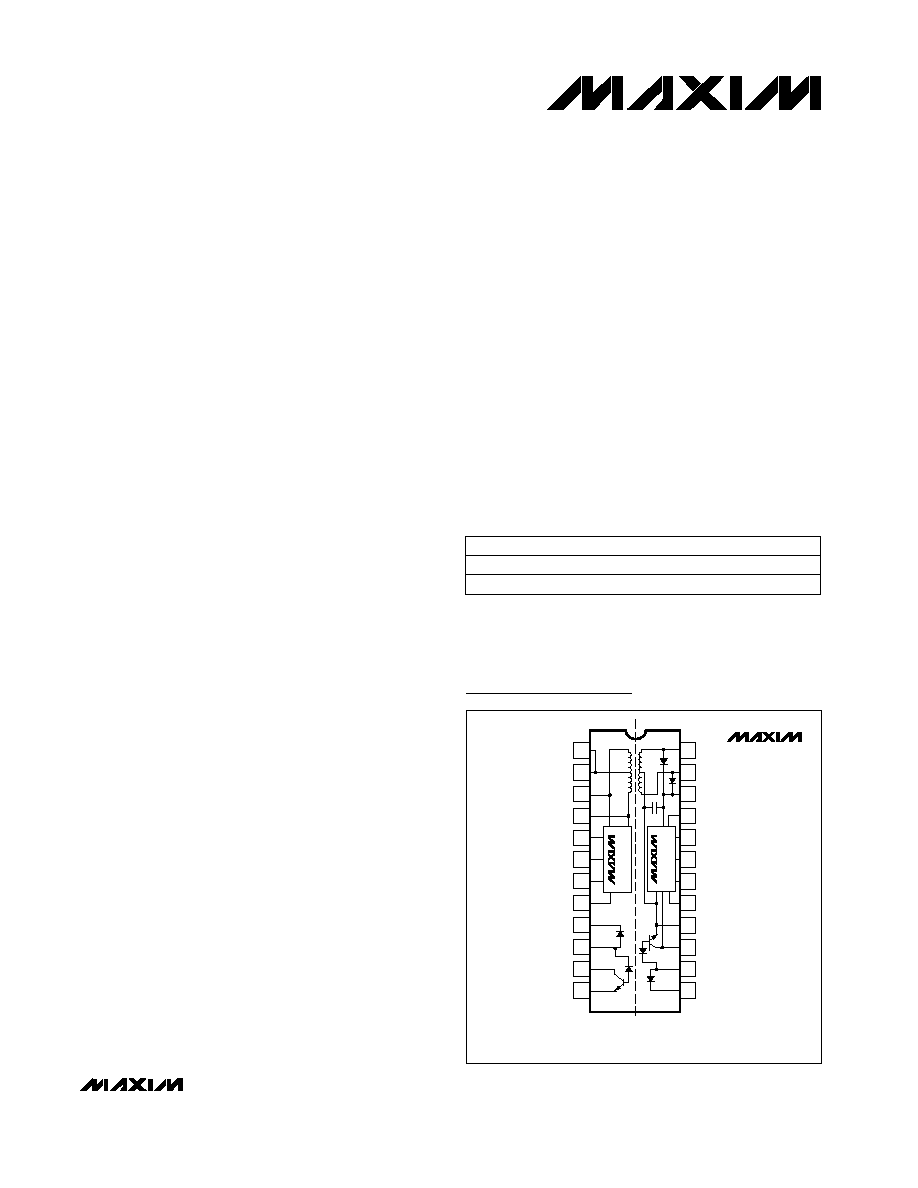
Pin Configurations
1
24
23
22
21
20
19
18
17
2
3
4
5
6
7
8
AC1
AC2
ISO V
CC1
ISO RO DRV
D2
D1
A
B
Z
Y
SD
FS
GND1
16
15
14
13
9
10
11
12
ISO COM1
ISO DI DRV
ISO V
CC2
ISO RO LED
GND2
RO
DI
DIP
V
CC2
V
CC3
V
CC4
V
CC1
MAX1490EA/
MAX1490EB
MAX845E
MAX488E MAX490E
TOP VIEW
ISOLATION BARRIER
19-1940; Rev 0; 4/01
PART
MAX1480EACPI
MAX1480EAEPI
-40°C to +85°C
0°C to +70°C
TEMP. RANGE
PIN-PACKAGE
28 Wide Plastic DIP*
28 Wide Plastic DIP*
_______________Ordering Information
Ordering Information continued at end of data sheet.
Data rate for A parts is up to 2.5Mbps. Data rate for C parts is
up to 250kbps.
*See Reliability section at end of data sheet.
Pin Configurations continued at end of data sheet.
Selector Guide appears at end of data sheet.
For pricing, delivery, and ordering information, please contact Maxim/Dallas Direct! at
1-888-629-4642, or visit Maxim's website at www.maxim-ic.com.
mA
MAX1480E/MAX1490E
±15kV ESD-Protected, Isolated RS-485/RS-422
Data Interfaces
2
_______________________________________________________________________________________
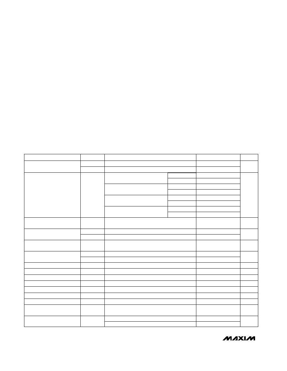
ABSOLUTE MAXIMUM RATINGS
ELECTRICAL CHARACTERISTICS
(V
CC_
= +5V ±10%, V
FS
= V
CC_
, T
A
= T
MIN
to T
MAX
, unless otherwise noted. Typical values are at V
CC_
= +5V and T
A
= +25°C.)
(Notes 1, 2)
Stresses beyond those listed under "Absolute Maximum Ratings" may cause permanent damage to the device. These are stress ratings only, and functional
operation of the device at these or any other conditions beyond those indicated in the operational sections of the specifications is not implied. Exposure to
absolute maximum rating conditions for extended periods may affect device reliability.
With Respect to GND_
Supply Voltage (V
CC_
)..........................................-0.3V to +6V
Control Input Voltage (SD, FS)..............-0.3V to (V
CC_
+ 0.3V)
Receiver Output Voltage (RO, RO).......-0.3V to (V
CC_
+ 0.3V)
Output Switch Voltage (D1, D2).......................................+12V
With Respect to ISO COM_
Control Input Voltage (ISO DE_) ....-0.3V to (ISO V
CC_
+ 0.3V)
Driver Input Voltage (ISO DI_) .......-0.3V to (ISO V
CC_
+ 0.3V)
Receiver Output Voltage (ISO RO_) ..-0.3V to (ISO V
CC_
+ 0.3V)
Driver Output Voltage (A, B, Y, Z) ......................-8V to +12.5V
Receiver Input Voltage (A, B).............................-8V to +12.5V
LED Forward Current (DI, DE, ISO RO LED) ......................50mA
Continuous Power Dissipation (T
A
= +70°C)
24-Pin Plastic DIP (derate 8.7mW°C above +70°C) ....696mW
28-Pin Plastic DIP (derate 9.09mW/°C above +70°C) .727mW
Operating Temperature Ranges
MAX1480E_CPI/MAX1490E_CPI ........................0°C to +70°C
MAX1480E_EPI/MAX1490E_EPI ......................-40°C to +85°C
Storage Temperature Range .............................-65°C to +150°C
Lead Temperature (soldering, 10s) .................................+300°C
Operating Supply Current
I
CC
1.5
5
R = 27
(RS-485), Figure 4
R = 50
(RS-422)
V
2
V
OD2
Differential Driver Output
(with Load)
V
FS
= 0
CONDITIONS
535
f
SWL
UNITS
MIN
TYP
MAX
SYMBOL
PARAMETER
FS = V
CC_
or open
725
f
SWH
85
120
55
120
MAX1480EA,
DE
´
= V
CC_
or open
145
130
Low
V
0.8
V
SDL
MAX1480EC,
DE
´
= V
CC_
or open
Shutdown Input Threshold
SD = V
CC_
High
µA
0.2
I
SHDN
Shutdown Supply Current
(Note 3)
2.4
V
SDH
120
65
125
High
Low
2.4
V
FSH
V
0.8
V
FSL
FS Input Threshold
DE
´
, DI
´
, Figures 1 and 2
DE
´
, DI
´
, Figures 1 and 2
V
V
CC
- 0.4
V
IH
Input High Voltage
V
0.4
V
IL
Input Low Voltage
FS low
FS high
µA
50
FS Input Pullup Current
pA
10
FS Input Leakage Current
pA
10
Shutdown Input Leakage
Current
R
L
=
R
L
= 54
R
L
=
R
L
= 54
R
L
=
MAX1490EB
R
L
= 54
T
A
= +25°C, f = 1MHz
pF
10
C
ISO
Isolation Capacitance
T
A
= +25°C, V
ISO
= 50VDC
M
100
10,000
R
ISO
Isolation Resistance
kHz
Switch Frequency
mA
R
L
=
R
L
= 54
130
180
MAX1490EA
180
V
8
V
OD1
Differential Driver Output
(No Load)
T
A
= +25°C, 1min (Note 4)
V
RMS
1260
V
ISO
Isolation Voltage
MAX1480E/MAX1490E
±15kV ESD-Protected, Isolated RS-485/RS-422
Data Interfaces
_______________________________________________________________________________________
3
ELECTRICAL CHARACTERISTICS (continued)
(V
CC_
= +5V ±10%, V
FS
= V
CC_
, T
A
= T
MIN
to T
MAX
, unless otherwise noted. Typical values are at V
CC_
= +5V and T
A
= +25°C.)
(Notes 1, 2)
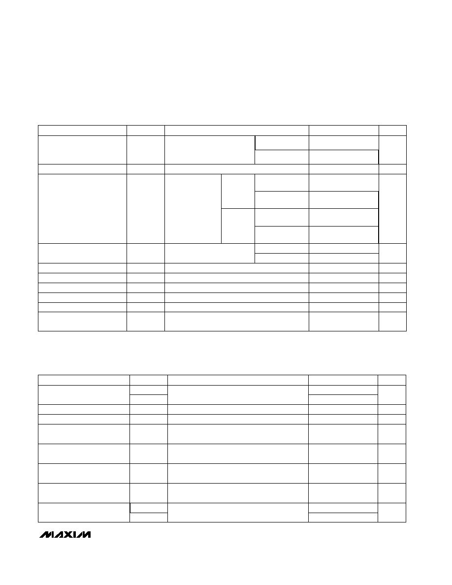
SWITCHING CHARACTERISTICS--MAX1480EA/MAX1490EA
(V
CC_
= +5V ±10%, V
FS
= V
CC_
, T
A
= T
MIN
to T
MAX
, unless otherwise noted. Typical values are at V
CC_
= +5V and T
A
= +25°C.)
Driver Disable Time from Low
(MAX1480EA Only)
t
LZ
0.5
1.8
µs
Figures 6 and 8, C
L
= 15pF, S1 closed
Driver Disable Time from High
(MAX1480EA Only)
t
HZ
0.5
1.8
µs
Figures 6 and 8, C
L
= 15pF, S2 closed
Driver Enable to Output Low
(MAX1480EA Only)
t
ZL
1.0
1.8
µs
Figures 6 and 8, C
L
= 100pF, S1 closed
PARAMETER
SYMBOL
MIN
TYP
MAX
UNITS
Driver Rise or Fall Time
t
R,
t
F
15
50
ns
Receiver Input to Output
Propagation Delay
t
PHL
90
225
ns
Figures 5 and 7, R
DIFF
= 54
, C
L1
= C
L2
= 100pF
t
PLH
120
225
Driver Enable to Output High
(MAX1480EA Only)
t
ZH
1.0
1.8
µs
Figures 5 and 10, R
DIFF
= 54
, C
L1
= C
L2
= 100pF
Figures 6 and 8, C
L
= 100pF, S2 closed
t
PLH
90
275
Figures 5 and 7, R
DIFF
= 54
,
C
L1
= C
L2
= 100pF
Driver Output Skew
CONDITIONS
t
SKEW
30
100
ns
Driver Input to Output
Propagation Delay
t
PHL
60
275
ns
Figures 5 and 7, R
DIFF
= 54
, C
L1
= C
L2
= 100pF
-7V
V
CM
+12V
V
V
TH
Receiver Differential Threshold
A, B, Y, and Z pins, tested using Human Body
Model, Figures 1 and 2
kV
ISO I
OSD
ESD Protection
R = 27
or 50, Figure 4
V
0.3
V
OD
CONDITIONS
Change in Magnitude of
Driver Output Voltage for
Complementary Output States
mA
0.25
R = 27
or 50, Figure 4
V
CM
= 0
k
R
IN
Receiver Input Resistance
mV
V
TH
Receiver Input Hysteresis
V
4
V
OC
Driver Common-Mode Output
1.0
UNITS
MIN
TYP
MAX
SYMBOL
PARAMETER
V
OUT
= 5.5V
µA
I
OH
Receiver Output High Current
Using resistor values listed in Tables 1 and 2
-7V
V
O
12V (Note 5)
mA
ISO I
OSD
Driver Short-Circuit Current
V
V
OL
Receiver Output Low Voltage
Differential
Common mode
0.3
MAX1490EA/
MAX1490EB
MAX1480EA/
MAX1480EC
MAX1480EA/
MAX1480EC
MAX1490EA/
MAX1490EB
0.2
ISO I
IN
Input Current (A, B)
0.8
DE
´
= 0,
V
CC_
= 0 or +5.5V
V
IN
= +12V
V
IN
= -7V
12
-0.2
0.2
70
0.4
250
100
±15
-7V
V
CM
+12V
48
(MAX1490E_)
(MAX1480E_)
MAX1480E/MAX1490E
±15kV ESD-Protected, Isolated RS-485/RS-422
Data Interfaces
4
_______________________________________________________________________________________
Note 1: All currents into device pins are positive; all currents out of device pins are negative. All voltages are referenced to logic-
side ground (GND_), unless otherwise specified.
Note 2: For DE
´
and DI
´
pin descriptions, see Detailed Block Diagram and Typical Application Circuit (Figure 1 for MAX1480EA/
MAX1480EC, Figure 2 for MAX1490EA/MAX1490EB).
Note 3: Shutdown supply current is the current at V
CC1
and V
CC2
when shutdown is enabled.
Note 4: Limit guaranteed by applying 1520V
RMS
for 1s. Test voltage is applied between all pins on one side of the package to all
pins on the other side of the package, e.g., between pins 114 and pins 1528 on the 28-pin package.
Note 5: Applies to peak current (see Typical Operating Characteristics). Although the MAX1480EA/MAX1480EC and
MAX1490EA/MAX1490EB provide electrical isolation between logic ground and signal paths, they do not provide isolation
between external shields and the signal paths (see Isolated Common Connection section).
SWITCHING CHARACTERISTICS--MAX1480EA/MAX1490EA (continued)
(V
CC_
= +5V ±10%, V
FS
= V
CC_
, T
A
= T
MIN
to T
MAX
, unless otherwise noted. Typical values are at V
CC_
= +5V and T
A
= +25°C.)
t
ZH(SHDN)
3
15
Figures 6 and 9, C
L
= 100pF, S2 closed
Shutdown to Driver Output High
t
ZH(SHDN)
3
15
µs
Figures 6 and 9, C
L
= 100pF, S1 closed
PARAMETER
SYMBOL
MIN
TYP
MAX
UNITS
CONDITIONS
Shutdown to Driver Output Low
µs
t
PLH
1.4
3.0
Figures 5 and 7, R
DIFF
= 54
, C
L1
= C
L2
= 100pF
Driver Input to Output
Propagation Delay
t
PHL
1.1
3.0
µs
Figures 5 and 7, R
DIFF
= 54
, C
L1
= C
L2
= 100pF
Driver Disable Time from High
(MAX1480EC Only)
t
HZ
1.7
4.5
µs
Figures 6 and 8, C
L
= 15pF, S2 closed
Driver Disable Time from Low
(MAX1480EC Only)
t
LZ
2.0
4.5
µs
Figures 6 and 8, C
L
= 15pF, S1 closed
Driver Enable to Output Low
(MAX1480EC Only)
t
ZL
1.4
4.5
µs
Figures 6 and 8, C
L
= 100pF, S1 closed
Driver Enable to Output High
(MAX1480EC Only)
t
ZH
1.4
4.5
µs
Figures 6 and 8, C
L
= 100pF, S2 closed
Time to Shutdown
t
SHDN
100
µs
PARAMETER
SYMBOL
MIN
TYP
MAX
UNITS
Driver Rise or Fall Time
t
R,
t
F
1.0
2.0
µs
|t
PLH
- t
PHL
| Differential
Receiver Skew
t
SKD
200
ns
Receiver Input to Output
Propagation Delay
t
PHL
1.1
3.0
µs
Figures 5 and 10, R
DIFF
= 54
, C
L1
= C
L2
= 100pF
Maximum Data Rate
Figures 5 and 7, R
DIFF
= 54
, C
L1
= C
L2
= 100pF
f
MAX
160
kbps
Shutdown to Driver Output Low
t
SKEW
, t
SKD
25% of data period
t
ZL(SHDN)
t
PLH
0.9
3.0
3
15
Figures 5 and 10, R
DIFF
= 54
, C
L1
= C
L2
= 100pF
µs
Figures 6 and 9, C
L
= 100pF, S1 closed
Shutdown to Driver Output High
t
ZH(SHDN)
3
15
µs
Figures 6 and 9, C
L
= 100pF, S2 closed
Driver Output Skew
CONDITIONS
t
SKEW
300
1200
ns
Figures 5 and 7, R
DIFF
= 54
, C
L1
= C
L2
= 100pF
t
SKD
30
150
Figures 5 and 10, R
DIFF
= 54
, C
L1
= C
L2
= 100pF
|t
PLH
- t
PHL
| Differential
Receiver Skew
ns
SWITCHING CHARACTERISTICS--MAX1480EC/MAX1490EB
(V
CC_
= +5V ±10%, V
FS
= V
CC_
, T
A
= T
MIN
to T
MAX
, unless otherwise noted. Typical values are at V
CC_
= +5V and T
A
= +25°C.)
t
SHDN
100
Time to Shutdown
µs
f
MAX
2.5
t
SKEW
, t
SKD
, t
PHL
25% of data period
Maximum Data Rate
Mbps
MAX1480E/MAX1490E
±15kV ESD-Protected, Isolated RS-485/RS-422
Data Interfaces
_______________________________________________________________________________________
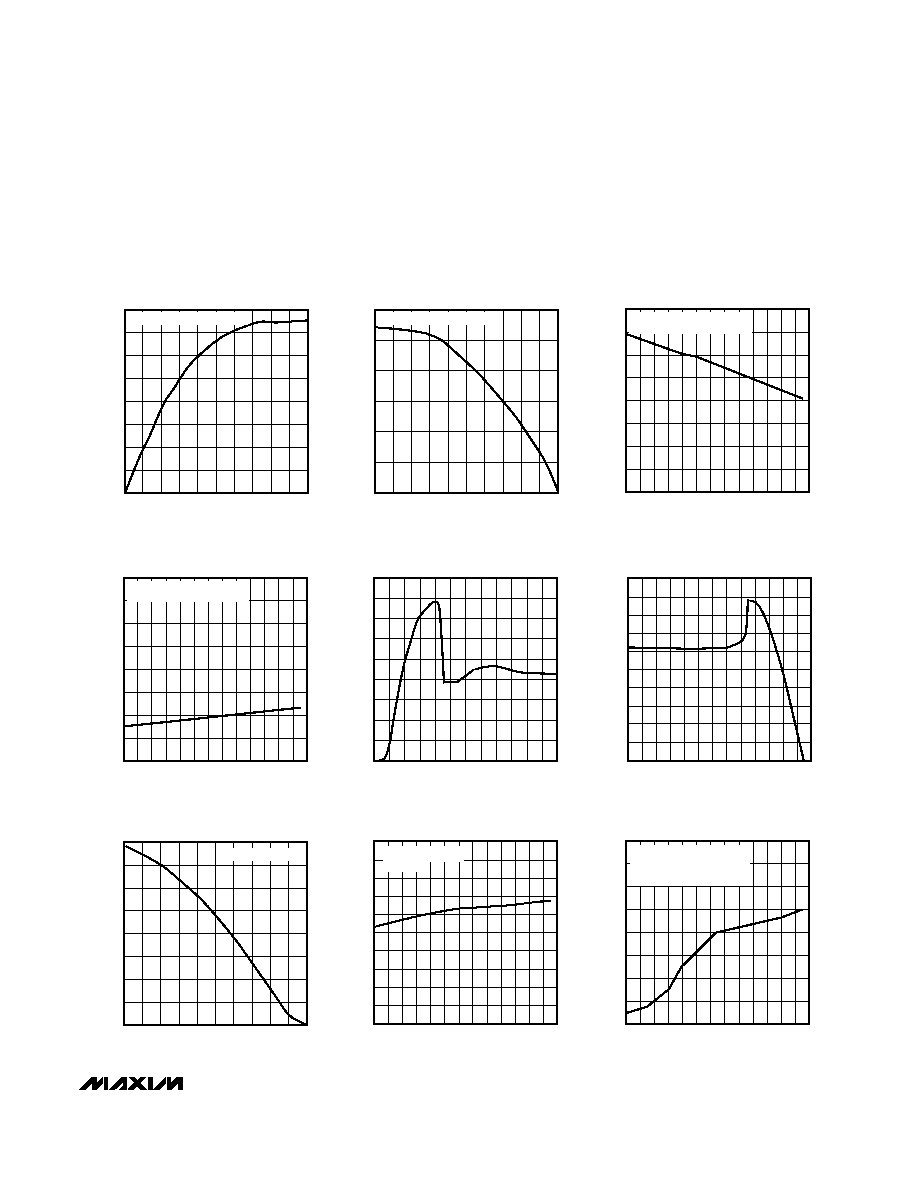
5
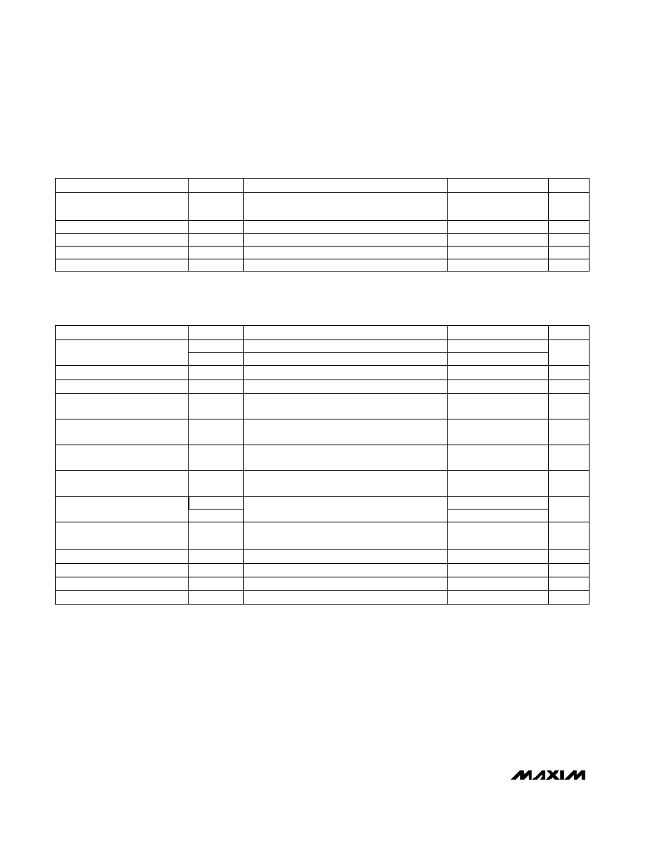
0
OUTPUT CURRENT vs.
RECEIVER OUTPUT LOW VOLTAGE
MAX1480E/90E TOC01
OUTPUT LOW VOLTAGE (V)
OUTPUT CURRENT (mA)
1.5
10
20
30
40
50
60
70
80
MEASURED AT ISO RO DRV
1.0
0.5
0
3.5
3.0
2.5
2.0
5.0
4.5
4.0
0
OUTPUT CURRENT vs.
RECEIVER OUTPUT HIGH VOLTAGE
MAX1480E/90E TOC02
OUTPUT HIGH VOLTAGE (V)
OUTPUT CURRENT (mA)
1.5
-5
MEASURED AT ISO RO DRV
1.0
0.5
0
3.5
3.0
2.5
2.0
5.0
4.5
4.0
-10
-15
-20
-25
-30
3.00
-40
20
RECEIVER OUTPUT HIGH VOLTAGE
vs. TEMPERATURE
MAX1480E/90E TOC03
TEMPERATURE (
°C)
OUTPUT HIGH VOLTAGE (V)
0
-20
60
40
80
3.25
3.50
3.75
4.00
4.25
4.50
4.75
5.00
MEASURED AT ISO RO DRV
I
RO
= 8mA
0
-40
20
RECEIVER OUTPUT LOW VOLTAGE
vs. TEMPERATURE
MAX1480E/90E TOC04
TEMPERATURE (
°C)
OUTPUT LOW VOLTAGE (V)
0
-20
60
40
80
0.1
0.2
0.3
0.4
0.5
0.6
0.7
0.8
MEASURED AT ISO RO DRV
I
RO
= 8mA
0
DRIVER OUTPUT CURRENT
vs. DIFFERENTIAL OUTPUT VOLTAGE
MAX1480E/90E TOC07
DIFFERENTIAL OUTPUT VOLTAGE (V)
OUTPUT CURRENT (mA)
1.5
10
20
30
40
50
60
70
80
DI
´
= HIGH OR OPEN
1.0
0.5
0
3.5
3.0
2.5
2.0
5.0
4.5
4.0
OUTPUT CURRENT vs.
DRIVER OUTPUT LOW VOLTAGE
MAX1480E/90E TOC05
OUTPUT LOW VOLTAGE (V)
OUTPUT CURRENT (mA)
0
160
180
140
100
120
80
40
60
0
20
1
2
3
4
5
6
7
8
9 10 11 12
0
-7
OUTPUT CURRENT vs.
DRIVER OUTPUT HIGH VOLTAGE
MAX1480E/90E TOC06
OUTPUT HIGH VOLTAGE (V)
OUTPUT CURRENT (mA)
0
-10
-20
-30
-40
-50
-60
-70
-80
-90
-100
-6 -5 -4 -3 -2 -1
1
2
3 4
5
6
2.0
-40
20
DRIVER DIFFERENTIAL OUTPUT VOLTAGE
vs. TEMPERATURE
MAX1480E/90E TOC08
TEMPERATURE (
°C)
DIFFERENTIAL OUTPUT VOLTAGE (V)
0
-20
60
40
80
2.1
2.2
2.3
2.4
2.5
2.6
2.7
2.8
2.9
3.0
DI
´
= HIGH OR OPEN
R
L
= 54
0
-40
20
SHUTDOWN CURRENT
vs. TEMPERATURE
MAX1480E/90E TOC09
TEMPERATURE (
°C)
SHUTDOWN CURRENT (
µ
A)
0
-20
60
40
80
0.05
0.10
0.15
0.20
0.25
0.30
0.35
0.40
SD = V
CC_
, DI
´
= V
CC_
DE
´
= V
CC_
(MAX1480EC ONLY)
MEASURED AT V
CC1
AND V
CC2
__________________________________________Typical Operating Characteristics
(V
CC_
= +5V, V
FS
= V
CC_
, Figures 1 and 2, T
A
= +25°C, unless otherwise noted.)