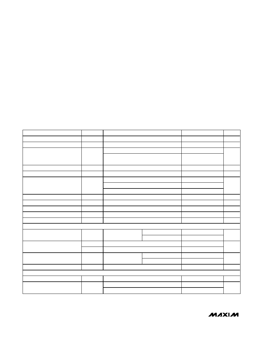
 | –≠–ª–µ–∫—Ç—Ä–æ–Ω–Ω—ã–π –∫–æ–º–ø–æ–Ω–µ–Ω—Ç: MAX1589A | –°–∫–∞—á–∞—Ç—å:  PDF PDF  ZIP ZIP |

General Description
The MAX1589A low-dropout linear regulator operates
from a +1.62V to +3.6V supply and delivers a guaran-
teed 500mA continuous load current with a low 175mV
dropout. The high-accuracy (±0.5%) output voltage is
preset to internally trimmed voltages from +0.75V to
+3.0V. An active-low, open-drain reset output remains
asserted for at least 70ms after the output voltage reach-
es regulation. This device is offered in 6-pin thin SOT23
and 6-pin, 3mm x 3mm thin DFN packages.
An internal pMOS pass transistor maintains low supply
current, independent of load and dropout voltage, making
the MAX1589A ideal for portable battery-powered equip-
ment such as personal digital assistants (PDAs), digital
still cameras, cell phones, cordless phones, and note-
book computers. Other features include logic-controlled
shutdown, short-circuit protection, and thermal-overload
protection.
Applications
Notebook Computers
Cellular and PCS Phones
Personal Digital Assistants (PDAs)
Handheld Computers
Digital Still Cameras
PCMCIA Cards
CD and MP3 Players
Features
o Low 1.62V Minimum Input Voltage
o Guaranteed 500mA Output Current
o ±0.5% Initial Accuracy
o Low 175mV Dropout at 500mA Load
o 70ms RESET Output Flag
o Supply Current Independent of Load and Dropout
Voltage
o Logic-Controlled Shutdown
o Thermal-Overload and Short-Circuit Protection
o Preset Output Voltages (0.75V, 1.0V, 1.3V, 1.5V,
1.8V, 2.5V, and 3.0V)
o Tiny 6-Pin Thin SOT23 Package (<1.1mm High)
o Thin 6-Pin TDFN Package (<0.8mm High)
MAX1589A
Low-Input-Voltage, 500mA LDO Regulator
with
R
RE
ES
SE
ET
T
in SOT and TDFN
________________________________________________________________ Maxim Integrated Products
1
GND
OUT
IN
TOP VIEW
MAX1589A
SHDN
GND
THIN SOT23
I.C.
RESET
RESET
1
2
3
6
5
4
4
5
6
SHDN
IN
3
2
1
I.C.
OUT
TDFN
3mm x 3mm
MAX1589A
Pin Configurations
ON
OFF
INPUT
1.62V TO 3.6V
IN
SHDN
GND
RESET
OUT
OUTPUT
0.75V TO 3.0V
500mA
TO
µC
LOGIC
SUPPLY
100k
MAX1589A
C
IN
1
µF
C
OUT
4.7
µF
Typical Operating Circuit
19-3664; Rev 0; 4/05
For pricing, delivery, and ordering information, please contact Maxim/Dallas Direct! at
1-888-629-4642, or visit Maxim's website at www.maxim-ic.com.
*Insert the desired three-digit suffix (see the Selector Guide) into
the blanks to complete the part number. Contact the factory for
other output voltages.
+Denotes lead-free packaging.
Selector Guide
MAX1589A
TOP MARK
V
OUT
(V)
SUFFIX
SOT
TDFN
0.75
075
AACC
ALG
1.00
100
AACD
ALH
1.30
130
AACE
ALI
1.50
150
AACF
ALJ
1.80
180
AACG
ALK
2.50
250
AACH
ALF
3.00
300
AACI
ALL
Ordering Information
PART*
TEMP RANGE
PIN-PACKAGE
MAX1589AEZT_ _ _+T
-40∞C to +85∞C
6 Thin SOT23-6
MAX1589AETT_ _ _ +
-40∞C to +85∞C
6 TDFN
MAX1589A
Low-Input-Voltage, 500mA LDO Regulator
with
R
RE
ES
SE
ET
T
in SOT and TDFN
2
_______________________________________________________________________________________
ABSOLUTE MAXIMUM RATINGS
Stresses beyond those listed under "Absolute Maximum Ratings" may cause permanent damage to the device. These are stress ratings only, and functional
operation of the device at these or any other conditions beyond those indicated in the operational sections of the specifications is not implied. Exposure to
absolute maximum rating conditions for extended periods may affect device reliability.
IN, SHDN, RESET to GND .....................................-0.3V to +4.0V
OUT to GND ................................................-0.3V to (V
IN
+ 0.3V)
Output Short-Circuit Duration.....................................Continuous
Continuous Power Dissipation (TA = +70∞C)
6-Pin Thin SOT23 (derate 9.1mW/∞C above +70∞C) ....727mW
6-Pin TDFN (derate 24.4mW/∞C above +70∞C) .........1951mW
Operating Temperature Range ...........................-40∞C to +85∞C
Junction Temperature ..................................................... +150∞C
Storage Temperature Range .............................-65∞C to +150∞C
Lead Temperature (soldering, 10s) .................................+300∞C
ELECTRICAL CHARACTERISTICS
(V
IN
= (V
OUT
+ 0.5V) or 1.8V, whichever is greater; SHDN = IN, C
IN
= 1µF, C
OUT
= 4.7µF, T
A
= -40∞C to +85∞C, unless otherwise
noted. Typical values are at T
A
= +25∞C.) (Note 1)
PARAMETER
SYMBOL
CONDITIONS
MIN
TYP
MAX
UNITS
Input Voltage
V
IN
1.62
3.60
V
Input Undervoltage Lockout
V
UVLO
V
IN
rising (180mV typical hysteresis)
1.30
1.60
V
I
OUT
= 150mA, T
A
= +25∞C
-0.5
+0.5
Output Voltage Accuracy
I
OUT
= 1mA to 500mA,
V
IN
= (V
OUT
+ 0.5V) to +3.6V
-1.5
+1.5
%
Maximum Output Current
I
OUT
Continuous
500
mA
RMS
Current Limit
I
LIM
V
OUT
= 96% of nominal value
550
850
1150
mA
No load
70
140
I
OUT
= 500mA
90
Ground Current
I
Q
Dropout (Note 2)
70
µA
Dropout Voltage
V
IN
- V
OUT
I
OUT
= 500mA, V
OUT
1.8V (Note 2)
175
350
mV
Load Regulation
V
LDR
I
OUT
= 1mA to 500mA
0.02
0.5
%
Line Regulation
V
LNR
V
IN
= (V
OUT
+ 0.5V) to +3.6V, I
OUT
= 100mA
-0.15
+0.01
+0.15
% / V
Output Noise
10Hz to 100kHz, I
OUT
= 10mA
86
µV
RMS
PSRR
f < 1kHz, I
OUT
= 10mA
70
dB
SHUTDOWN
T
A
= +25∞C
0.001
1
Shutdown Supply Current
I
OFF
SHDN = GND
T
A
= +85∞C
0.01
µA
V
IH
V
IN
= 1.62V to 3.6V
1.4
SHDN Input Logic Levels
V
IL
V
IN
= 1.62V to 3.6V
0.6
V
T
A
= +25∞C
1
300
SHDN Input Bias Current
I
SHDN
V
SHDN
= 0V or 3.6V
T
A
= +85∞C
5
nA
Turn-On Delay
From SHDN high to OUT high, V
OUT
= 1.5V
90
µs
RESET OUTPUT
Reset Threshold Accuracy
V
OUT
falling (1.7% typical hysteresis)
80
82.5
85
%V
OUT
I
RESET
= 100µA
1.5
100
RESET Output Low Voltage
V
OL
V
IN
= +1.0V, I
RESET
= 100µA
3
100
mV

MAX1589A
Low-Input-Voltage, 500mA LDO Regulator
with
R
RE
ES
SE
ET
T
in SOT and TDFN
_______________________________________________________________________________________
3
Note 1: Limits are 100% production tested at T
A
= +25∞C. Limits over the operating temperature range are guaranteed by design.
Note 2: The dropout voltage is defined as V
IN
- V
OUT
, when V
OUT
is 4% lower than the value of V
OUT
when V
IN
= V
OUT
+ 0.5V.
ELECTRICAL CHARACTERISTICS (continued)
(V
IN
= (V
OUT
+ 0.5V) or 1.8V, whichever is greater; SHDN = IN, C
IN
= 1µF, C
OUT
= 4.7µF, T
A
= -40∞C to +85∞C, unless otherwise
noted. Typical values are at T
A
= +25∞C.) (Note 1)
PARAMETER
SYMBOL
CONDITIONS
MIN
TYP
MAX
UNITS
T
A
= +25∞C
0.001
1
RESET Output High
Leakage Current
I
OH
V
RESET
= 3.6V,
RESET not asserted
T
A
= +85∞C
0.01
µA
Reset Delay
t
RP
From V
OUT
high to RESET rising
70
100
160
ms
THERMAL PROTECTION
Thermal-Shutdown Temperature
T
SHDN
+165
∞C
Thermal-Shutdown Hysteresis
T
SHDN
15
∞C
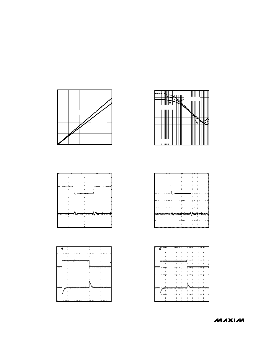
OUTPUT VOLTAGE ACCURACY
vs. LOAD CURRENT
MAX1589A toc01
LOAD CURRENT (mA)
OUTPUT VOLTAGE ACCURACY (%)
400
300
200
100
-0.1
0
0.1
0.2
-0.2
0
500
V
OUT
= +3.0V
V
OUT
= +1.5V
V
OUT
= +0.75V
OUTPUT VOLTAGE ACCURACY
vs. INPUT VOLTAGE
MAX1589A toc02
INPUT VOLTAGE (V)
OUTPUT VOLTAGE ACCURACY (%)
3.4
3.0
2.6
2.2
1.8
-0.25
0
0.25
0.50
-0.50
1.4
V
OUT
= +1.5V
I
OUT
= 0mA
I
OUT
= 100mA
I
OUT
= 500mA
OUTPUT VOLTAGE ACCURACY
vs. TEMPERATURE
MAX1589A toc03
TEMPERATURE (
∞C)
OUTPUT VOLTAGE ACCURACY (%)
60
35
10
-15
-1.0
-0.5
0
0.5
1.0
1.5
-1.5
-40
85
V
OUT
= +1.5V
I
OUT
= 0mA, 100mA, 500mA
120
60
0.01
0.1
1
10
100
1000
GROUND-PIN CURRENT
vs. LOAD CURRENT
MAX1589A toc04
LOAD CURRENT (mA)
GROUND-PIN CURRENT (
µ
A)
100
110
70
80
90
V
OUT
= +3.0V
V
OUT
= +1.5V
V
OUT
= +0.75V
GROUND-PIN CURRENT
vs. INPUT VOLTAGE
MAX1589A toc05
INPUT VOLTAGE (V)
GROUND-PIN CURRENT (
µ
A)
3.2
2.8
2.4
2.0
1.6
20
40
60
80
100
120
0
1.2
3.6
I
OUT
= 0mA
I
OUT
= 500mA
I
OUT
= 100mA
V
OUT
= +1.5V
GROUND-PIN CURRENT
vs. TEMPERATURE
MAX1589A toc06
TEMPERATURE (
∞C)
GROUND-PIN CURRENT (
µ
A)
60
35
10
-15
60
70
80
90
100
50
-40
85
V
OUT
= +1.5V
I
OUT
= 1mA TO 500mA
I
OUT
= 0mA
Typical Operating Characteristics
(V
IN
= (V
OUT
+ 0.5V) or 1.8V, whichever is greater; SHDN = IN, C
IN
= 1µF, C
OUT
= 4.7µF, T
A
= +25∞C, unless otherwise noted.)
MAX1589A
Low-Input-Voltage, 500mA LDO Regulator
with
R
RE
ES
SE
ET
T
in SOT and TDFN
4
_______________________________________________________________________________________
DROPOUT VOLTAGE
vs. LOAD CURRENT
MAX1589A toc07
LOAD CURRENT (mA)
V
DROPOUT
(mV)
400
300
200
100
40
80
120
160
200
0
0
500
V
OUT
= +1.8V
V
OUT
= +3.0V
Typical Operating Characteristics (continued)
(V
IN
= (V
OUT
+ 0.5V) or 1.8V, whichever is greater; SHDN = IN, C
IN
= 1µF, C
OUT
= 4.7µF, T
A
= +25∞C, unless otherwise noted.)
POWER-SUPPLY REJECTION RATIO
vs. FREQUENCY
FREQUENCY (kHz)
PSRR (dB)
100
10
1
10
20
30
40
50
60
70
80
0
0.1
1000
I
OUT
= 10mA
V
OUT
= +3.0V
V
OUT
= +1.5V
V
OUT
= +0.75V
MAX1589A toc08
LINE-TRANSIENT RESPONSE
MAX1589A toc09
40
µs/div
3.5V
4V
1.5V
10mV/div
AC-COUPLED
500mV/div
V
OUT
V
IN
I
LOAD
= 100mA
V
OUT
= 1.5V
LINE-TRANSIENT RESPONSE
NEAR DROPOUT
MAX1589A toc10
40
µs/div
1.8V
2.5V
1.5V
10mV/div
AC-COUPLED
500mV/div
V
OUT
V
IN
I
LOAD
= 100mA
V
OUT
= 1.5V
LOAD-TRANSIENT RESPONSE
MAX1589A toc12
20
µs/div
100mA
500mA
50mV/div
AC-COUPLED
500mA/div
V
OUT
I
OUT
V
IN
= 3.6V
V
OUT
= 1.5V
LOAD-TRANSIENT RESPONSE
MAX1589A toc11
20
µs/div
20mA
200mA
20mV/div
AC-COUPLED
200mA/div
V
OUT
I
OUT
V
IN
= 1.8V
V
OUT
= 1.5V
0

MAX1589A
Low-Input-Voltage, 500mA LDO Regulator
with
R
RE
ES
SE
ET
T
in SOT and TDFN
_______________________________________________________________________________________
5
SHUTDOWN RESPONSE
MAX1589A toc13
100
µs/div
0
0
500mV/div
1V/div
V
OUT
V
SHDN
R
L
= 25
V
OUT
= 1.5V
Typical Operating Characteristics (continued)
(V
IN
= (V
OUT
+ 0.5V) or 1.8V, whichever is greater; SHDN = IN, C
IN
= 1µF, C
OUT
= 4.7µF, T
A
= +25∞C, unless otherwise noted.)
SHUTDOWN/RESET RESPONSE
MAX1589A toc14
40ms/div
0
0
0
1V/div
1V/div
1V/div
V
RESET
V
OUT
V
SHDN
R
L
= 25
V
OUT
= 1.5V
LINE/RESET RESPONSE
MAX1589A toc15
200ms/div
0
0
0
2V/div
1V/div
1V/div
V
RESET
V
OUT
V
IN
R
L
= 25
V
OUT
= 1.5V