
General Description
The MAX2900≠MAX2904 complete single-chip 200mW
transmitters are designed for use in the 868MHz/
915MHz frequency bands. The MAX2900/MAX2901/
MAX2902 are compliant with the FCC CFR47 part 15.247
902MHz to 928MHz ISM-band specifications. MAX2903/
MAX2904 are compliant with the ETSI EN330-220 speci-
fication for the European 868MHz ISM band.
These transmitter ICs offer a high level of integration
while minimizing the number of external components.
This is achieved by full integration of the transmit modu-
lator, power amplifier, RF VCO, 8-channel frequency syn-
thesizer, and baseband PN sequence lowpass filter. By
filtering the BPSK modulation, the spurious emissions are
reduced, enabling up to eight independent transmit
channels in the U.S. ISM band. Inputs are provided for
spread-spectrum BPSK, ASK, and OOK. FM can be
achieved by directly modulating the VCO. The devices
are intended primarily for use with an external differential
antenna.
Applications
Automatic Meter Reading
Wireless Security Systems/Alarms
Wireless Sensors
Wireless Data Networks
Wireless Building Control
Features
o Versions for U.S. 902MHz to 928MHz Band and
European 868MHz Band
o -7dBm to +23dBm Adjustable Differential RF
Output Power
o +23dBm Output Power at 4.5V, +20dBm Output
Power at 3.0V
o Support BPSK, OOK, ASK, and FM Modulations
o Modulation Filter for Direct Sequence BPSK up to
8Mchips/s
o Fully Integrated VCO with On-Chip Tank
o Extremely Low Frequency Pulling for OOK
Modulation (typ 60kHz peak, 5kHz RMS)
o Integrated Frequency Synthesizer for up to
8 Channels (MAX2900)
o +2.7V to +4.5V Supply Operation
o Small 28-Pin QFN Package with Exposed Pad
(5mm
5mm)
MAX2900≠MAX2904
200mW Single-Chip Transmitter ICs for
868MHz/915MHz ISM Bands
________________________________________________________________ Maxim Integrated Products
1
1
3
2
4
5
6
7
21
19
20
18
17
16
15
8
10
9
11
12
13
14
28
26
27
25
24
23
22
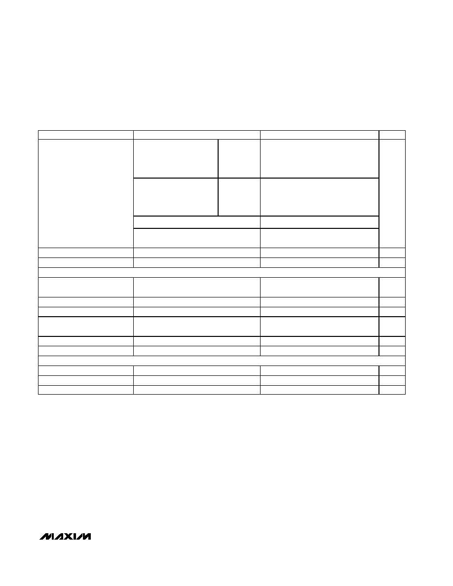
REFEN
EN
RLPF
VCC1
VREG
GND
VTUNE
GND
RF-
RF+
GND
DIVOUT
VCO-
VCO+
OSC
REFIN
VCC4
REFOUT
DIV63
VCC5
CPOUT
VCC3
PWRSET
LD
VASK
VCC2
OOKIN
MODIN
DUAL-
CHANNEL
(/62 OR /63)
SYNTHESIZER
CP
GATE
REG
MAX2901/
MAX2903
1
3
2
4
5
6
7
21
19
20
18
17
16
15
8
10
9
11
12
13
14
28
26
27
25
24
23
22
REFEN
EN
RLPF
VCC1
VREG
GND
VTUNE
GND
RF-
RF+
N.C.
N.C.
D1
D0
OSC
REFIN
VCC4
REFOUT
D2
VCC5
CPOUT
VCC3
PWRSET
LD
VASK
VCC2
OOKIN
MODIN
8-CHANNEL
SYNTHESIZER
CP
GATE
REG
˜4
MAX2900
Functional Diagrams/Pin Configurations
19-2145; Rev 1; 8/03
Ordering Information
*Exposed pad
PART
TEMP RANGE
PIN-PACKAGE
MAX2900EGI
-40∞C to +85∞C
28 QFN-EP*
MAX2901EGI
-40∞C to +85∞C
28 QFN-EP*
MAX2902EGI
-40∞C to +85∞C
28 QFN-EP*
MAX2903EGI
-40∞C to +85∞C
28 QFN-EP*
MAX2904EGI
-40∞C to +85∞C
28 QFN-EP*
Functional Diagrams/Pin Configurations are continued at end of data sheet.
For pricing, delivery, and ordering information, please contact Maxim/Dallas Direct! at
1-888-629-4642, or visit Maxim's website at www.maxim-ic.com.

MAX2900≠MAX2904
200mW Single-Chip Transmitter ICs for
868MHz/915MHz ISM Bands
2
_______________________________________________________________________________________
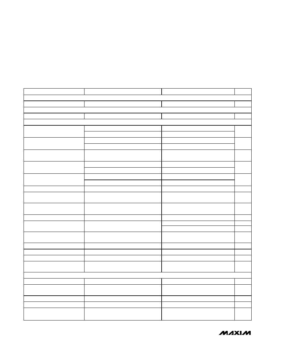
ABSOLUTE MAXIMUM RATINGS
DC ELECTRICAL CHARACTERISTICS
(V
CC
= +2.7V to +4.5V, EN = OOKIN = REFEN = high, T
A
= -40∞C to +85∞C. Typical values are at V
CC
= +4.5V, T
A
= +25∞C, unless
otherwise noted.) (Note 1)
Stresses beyond those listed under "Absolute Maximum Ratings" may cause permanent damage to the device. These are stress ratings only, and functional
operation of the device at these or any other conditions beyond those indicated in the operational sections of the specifications is not implied. Exposure to
absolute maximum rating conditions for extended periods may affect device reliability.
V
CC
to GND ...........................................................-0.3V to +5.0V
Analog/Digital Input Voltage to GND..........-0.3V to (V
CC
+ 0.3V)
Analog/Digital Input Current ..............................................±10µA
Continuous Power Dissipation (T
A
= +70∞C)
28-Pin QFN-EP (derate 28.5mW/∞C above +70∞C)............2W
Operating Temperature Range ...........................-40∞C to +85∞C
Junction Temperature .....................................................+150∞C
Storage Temperature Range .............................-65∞C to +150∞C
Lead Temperature (soldering, 10s) .................................+300∞C
PARAMETER
CONDITIONS
MIN
-3
TYP
+3
MAX
UNITS
Supply Voltage
2.7
4.5
4.5
V
V
CC
= +4.0V
0.7
10
Shutdown mode: EN =
REFEN = low
V
CC
= +4.5V
60
200
µA
Synth mode: OOKIN = low
(MAX2900/MAX2901/MAX2903 only)
32
40
Transmit mode with output
matching optimized for
+23dBm at +4.5V: PWRSET
loaded with 22k
resistor
T
A
= -40∞C
to +85∞C
150
200
Supply Current
Transmit mode with output
matching optimized for
+20dBm at +3.0V: PWRSET
loaded with 22k
resistor
T
A
= -40∞C
to +85∞C
110
135
mA
Five different versions are available. The versions differ
by their frequency band of operation, and by the synthe-
sizer's mode of operation. The MAX2900 has an internal
8-channel synthesizer.
The MAX2901 and MAX2903 are dual-channel versions
with a selectable internal synthesizer division ratio of 62
or 63. The MAX2901 operates in the 902MHz to
928MHz ISM band and the MAX2903 operates in the
867MHz to 870MHz European ISM band.
The MAX2902 and MAX2904 require an off-chip fre-
quency synthesizer. The MAX2902 operates in the
902MHz≠ 928MHz ISM band and MAX2904 operates in
the 867MHz≠870MHz European ISM band.
The MAX2901≠MAX2904 provide LO outputs to drive a
receiver and/or an external synthesizer.
PART
FREQUENCY RANGE (MHz)
SYNTHESIZER
LO OUTPUTS
MAX2900EGI
902 to 928
Internal 8 selectable channels
No
MAX2901EGI
902 to 928
Internal 2 selectable channels
Yes
MAX2902EGI
902 to 928
Off-chip
Yes
MAX2903EGI
867 to 870
Internal 2 selectable channels
Yes
MAX2904EGI
867 to 870
Off-chip
Yes
Part Selection Information
CAUTION! ESD SENSITIVE DEVICE
MAX2900≠MAX2904
200mW Single-Chip Transmitter ICs for
868MHz/915MHz ISM Bands
_______________________________________________________________________________________
3
DC ELECTRICAL CHARACTERISTICS (continued)
(V
CC
= +2.7V to +4.5V, EN = OOKIN = REFEN = high, T
A
= -40∞C to +85∞C. Typical values are at V
CC
= +4.5V, T
A
= +25∞C, unless
otherwise noted.) (Note 1)
PARAMETER
CONDITIONS
MIN
-3
TYP
+3
MAX
UNITS
Transmit mode with output
matching optimized for
+17dBm at +3.0V: PWRSET
loaded with 36k
resistor
T
A
= +25∞C
75
Transmit mode with output
matching optimized for
+14dBm at +3.0V: PWRSET
loaded with 51k
resistor
T
A
= +25∞C
57
Reference-only mode: EN = low
2
3
Supply Current (continued)
PA standby mode: OOKIN = low
(MAX2902/MAX2904 only)
29
33
mA
VCO Input Tuning Pin Current
VTUNE = +4.5V, T
A
= +25∞C
0.02
2
µA
VREG VCO Regulator Voltage
2.0
V
D IG IT A L IN PU T /O U T PU T S ( P IN S E N , RE FE N , D 0, D 1, D 2, M O D IN , O OKIN , LD )
Input Level High
V
CC
- 0.5V
V
Input Level Low
0.5
V
Input Bias Current
-10
10
µA
Output Level High
V
CC
- 0.4
V
Output Level Low
0.4
V
Output Current
-100
100
µA
ANALOG CONTROL INPUTS (PINS PWRSET, RLPF, VASK)
PWRSET Voltage
1.2
V
RLPF Voltage
1.2
V
VASK Input Impedance
100
220
400
k
MAX2900≠MAX2904
200mW Single-Chip Transmitter ICs for
868MHz/915MHz ISM Bands
4
_______________________________________________________________________________________
AC ELECTRICAL CHARACTERISTICS
(MAX290_ EV kits. V
CC
= +2.7V to +4.5V, R
RLPF
= 68k
, R
PWRSET
= 22k
, f
RF
= 917.28MHz (MAX2900/MAX2901/MAX2902) or f
RF
= 868MHz (MAX2903/MAX2904), VASK = VREG, f
REF
= 14.56MHz (MAX2900/MAX2901/MAX2902) or f
REF
= 13.62MHz
(MAX2903/MAX2904), chip rate on MODIN = 1.22Mbps, P
OUT
= +23dBm, T
A
= -40∞C to +85∞C. Typical values are at V
CC
= +4.5V,
T
A
= +25∞C, unless otherwise noted.) (Note 1)
PARAMETER
CONDITIONS
MIN
-3
TYP
+3
MAX
U N I T S
ANALOG INPUT PINS
VTUNE Input Capacitance
VTUNE = +1.35V
15
p F
DIGITAL INPUT PINS
Digital Input Pin Capacitance
3
p F
VCO AND SYNTHESIZERS SECTION
(MAX2900/MAX2901/MAX2902)
902
917.28
928
RFOUT Frequency Range
(MAX2903/MAX2904)
867
868
870
M H z
(MAX2900/MAX2901/MAX2902)
14
14.56
15
REFIN Reference Frequency
Range
(MAX2903/MAX2904)
13
13.78
14.5
M H z
REFDIV Fixed Reference Divider
Ratio
(MAX2900)
4
4
4
Table 4 (MAX2900)
249
256
Main Divider Ratios
(MAX2901/MAX2903)
62
63
(MAX2900)
3.5
3.64
3.75
PLL Comparison Frequency
(MAX2901/MAX2903)
13
15
M H z
VCO Buffer Output Power
300
differential load (MAX2901≠MAX2904)
-12
d Bm
REFDIV Fixed Reference
Divider Ratio
(MAX2901/MAX2903)
1
1
1
VCO Phase Noise
At 100kHz offset, measured at RFOUT,
PLL loop BW = 5kHz
-101
d Bc/H z
VCO Tuning Gain
VTUNE = +1.35V
44
65
86
M H z/V
5
kH z RM S
VCO Frequency Pulling with
OOK Modulation
OOKIN clocked at 19kHz, internal (crystal)
or external reference frequency
60
kH z p eak
PLL Phase Noise
Measured at RFOUT, 5kHz offset,
PLL loop BW = 50kHz
-96
d Bc/H z
REFOUT Voltage Swing
100
m V p - p
CPOUT Charge Pump Current
500
µA
Reference Spurs
-62
d Bc
Reference Input Voltage for
Nominal Operation
Using an external frequency reference
200
300
m V
BPSK, OOK MODULATOR, AND PA
MODIN Frequency Range
1.2
8
M b /s
Modulation Filter Nominal 3dB
Bandwidth
1
M H z
Modulation Filter Final Attenuation Measured at 30MHz
28
41
d B
Carrier Suppression
28
d B
Noise Power Density
At 960MHz (measured at RFOUT at
+23dBm output power)
-150
d Bc/H z

MAX2900≠MAX2904
200mW Single-Chip Transmitter ICs for
868MHz/915MHz ISM Bands
_______________________________________________________________________________________
5
AC ELECTRICAL CHARACTERISTICS (continued)
(MAX290_ EV kits. V
CC
= +2.7V to +4.5V, R
RLPF
= 68k
, R
PWRSET
= 22k
, f
RF
= 917.28MHz (MAX2900/MAX2901/MAX2902) or f
RF
= 868MHz (MAX2903/MAX2904), VASK = VREG, f
REF
= 14.56MHz (MAX2900/MAX2901/MAX2902) or f
REF
= 13.62MHz
(MAX2903/MAX2904), chip rate on MODIN = 1.22Mbps, P
OUT
= +23dBm, T
A
= -40∞C to +85∞C. Typical values are at V
CC
= +4.5V,
T
A
= +25∞C, unless otherwise noted.) (Note 1)
PARAMETER
CONDITIONS
MIN
-3
TYP
+3
MAX
U N I T S
PWRSET = 22k
, V
CC
= +4.5V,
T
A
= +25∞C
21
23.5
25
PWRSET = 22k
, V
CC
= +4.5V,
T
A
= -40∞C to +85∞C
20.5
25
RF Output Power
P WRS E T = 22k
, V
C C
= + 3.0V , T
A
= + 25∞C 18
20
21
d Bm
f
RF
= 900MHz to 930MHz
(MAX2900/MAX2901/MAX2902)
0.3
RF Output Power Flatness
f
RF
= 867MHz to 870MHz
0.1
d B
Adjacent Channel Power Ratio
PN sequence at 1.22MHz
-17
d Bc
Alternate Channel Power Ratio
PN sequence at 1.22MHz
-26
d Bc
OOK Control Range
40
80
d B
OOKIN = high,
VASK = 0
41
ASK Output Power Adjustment
Range
ASK output power back-
off relative to max power
OOKIN = high,
VASK = 1V
16
d B
RFOUT Rise and Fall Time
Square-wave signal applied on OOK
1
µs
At 2nd harmonic of RF output frequency
with external matching network
-50
At 3rd harmonic of RF output frequency
with external matching network
-51
At 4th harmonic of RF output frequency
with external matching network
-63
Out of 902MHz to 928MHz band other than
harmonics with external matching network
(MAX2900/MAX2901/MAX2902)
< -70
Spurious Emissions
Out of 867MHz to 870MHz band other than
harmonics with external matching network
(MAX2903/MAX2904)
< -70
d Bc
Unlocked, Out-of-Band Spurious
Output Level
Any condition when synthesizer unlocked
(pin LD low)
< -50
d Bm
Modulation off, measured at 960MHz, any
gain setting (MAX2900/MAX2901/MAX2902)
-126
-120
Noise Level Out of Band
Modulation off, measured at 900MHz, any
gain setting (MAX2903/MAX2904)
-126
-120
d Bm /H z
Output VSWR for Guaranteed
Stability
2:1
M axi m um Al l ow ab l e Outp ut V S WR
2:1
Note 1: Devices are production tested at T
A
= +25∞C and +85∞C. Min/Max values are guaranteed by design and characterization
over temperature and supply voltage.