 | –≠–ª–µ–∫—Ç—Ä–æ–Ω–Ω—ã–π –∫–æ–º–ø–æ–Ω–µ–Ω—Ç: MAX3691 | –°–∫–∞—á–∞—Ç—å:  PDF PDF  ZIP ZIP |
_______________General Description
The MAX3691 serializer is ideal for converting 4-bit-
wide, 155Mbps parallel data to 622Mbps serial data in
ATM and SDH/SONET applications. Operating from a
single +3.3V supply, this device accepts low-voltage
differential-signal (LVDS) clock and data inputs for
interfacing with high-speed digital circuitry, and deliv-
ers a 3.3V PECL serial-data output. A fully integrated
PLL synthesizes an internal 622Mbps serial clock from
a 155.52MHz reference clock.
The MAX3691 is available in the extended-industrial
temperature range (-40∞C to +85∞C), in a 32-pin TQFP
package.
________________________Applications
622Mbps SDH/SONET Transmission Systems
622Mbps ATM/SONET Access Nodes
Add/Drop Multiplexers
Digital Cross Connects
____________________________Features
o
Single +3.3V Supply
o
155Mbps Parallel to 622Mbps Serial Conversion
o
215mW Power
o
LVDS Parallel Clock and Data Inputs
o
Differential 3.3V PECL Serial-Data Output
MAX3691
+3.3V, 622Mbps, SDH/SONET 4:1 Serializer
with Clock Synthesis and LVDS Inputs
________________________________________________________________
Maxim Integrated Products
1
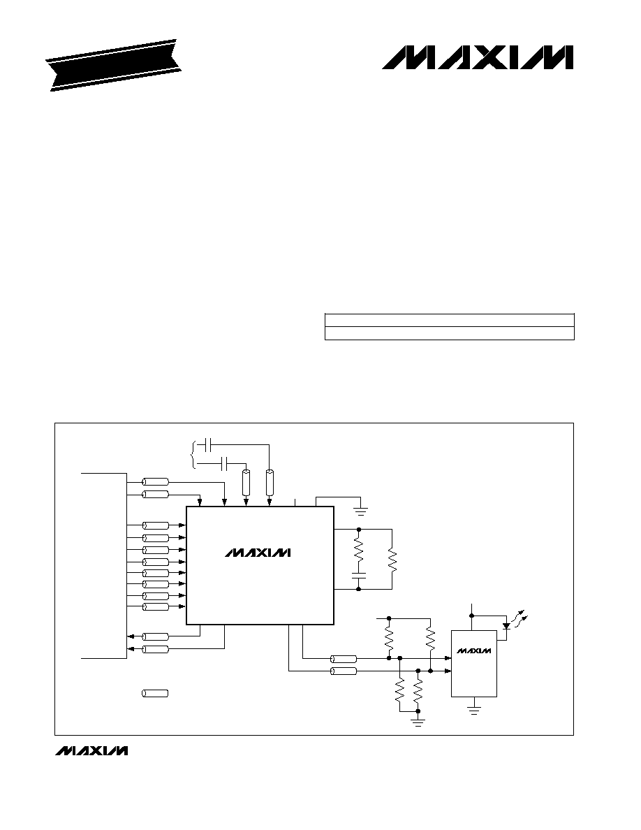
MAX3691
MAX3667
SD-
PCLKO- PCLKO+
LVDS CRYSTAL REFERENCE
PCLKI- PCLKI+ RCLK-
0.1µF
0.1µF
V
CC
GND
SD+
FIL-
FIL+
130
130
82
1.5k
100pF
24.9k
82
V
CC
= +3.3V
V
CC
= +3.3V
V
CC
= +3.3V
OVERHEAD
GENERATION
PD3-
PD3+
PD2-
PD2+
PD1-
PD1+
PD0-
PD0+
THIS SYMBOL REPRESENTS A TRANSMISSION LINE
OF CHARACTERISTIC IMPEDANCE (Z
0
= 50
)
RCLK+
___________________________________________________Typical Operating Circuit
19-1207; Rev 0; 3/97
PART
MAX3691ECJ
-40∞C to +85∞C
TEMP. RANGE
PIN-PACKAGE
32 TQFP
______________Ordering Information
For free samples & the latest literature: http://www.maxim-ic.com, or phone 1-800-998-8800
Pin Configuration appears at end of data sheet.
EVALUATION KIT
AVAILABLE

MAX3691
+3.3V, 622Mbps, SDH/SONET 4:1 Serializer
with Clock Synthesis and LVDS Inputs
2
_______________________________________________________________________________________
ABSOLUTE MAXIMUM RATINGS
DC ELECTRICAL CHARACTERISTICS
(V
CC
= +3.0V to +3.6V, differential LVDS loads = 100
±1%, PECL loads = 50
±1% to (V
CC
- 2V), T
A
= -40∞C to +85∞C, unless
otherwise noted. Typical values are at V
CC
= +3.3V, T
A
= +25∞C.)
Stresses beyond those listed under "Absolute Maximum Ratings" may cause permanent damage to the device. These are stress ratings only, and functional
operation of the device at these or any other conditions beyond those indicated in the operational sections of the specifications is not implied. Exposure to
absolute maximum rating conditions for extended periods may affect device reliability.
Terminal Voltage (with respect to GND)
V
CC
.........................................................................-0.5V to 5V
All Inputs.................................................-0.5V to (V
CC
+ 0.5V)
Output Current
LVDS Outputs (PCLKO±)................................................10mA
PECL Outputs (SD±).......................................................50mA
Continuous Power Dissipation (T
A
= +85∞C)
TQFP (derate 10.20mW/∞C above +85∞C) ...................663mW
Operating Temperature Range ...........................-40∞C to +85∞C
Storage Temperature Range .............................-65∞C to +160∞C
Lead Temperature (soldering, 10sec) .............................+300∞C
T
A
= +25∞C to +85∞C
PECL outputs unterminated
T
A
= +25∞C to +85∞C
Differential input voltage =
100mV
Common-mode voltage =
50mV
CONDITIONS
V
V
CC
- 1.03 V
CC
- 0.88
V
OH
Output High Voltage
mA
38
65
100
I
CC
Supply Current
V
0.925
V
OL
Output Low Voltage
V
1.475
V
OH
Output High Voltage
85
100
115
R
IN
Differential Input Resistance
mV
70
V
HYST
Threshold Hysteresis
V
V
CC
- 1.81 V
CC
- 1.62
V
OL
Output Low Voltage
V
0
2.4
V
I
Input Voltage Range
mV
-100
100
V
IDTH
Differential Input Threshold
UNITS
MIN
TYP
MAX
SYMBOL
PARAMETER
%
±1
±10
R
O
Change in Magnitude of Single-Ended Output
Resistance for Complementary States
40
70
140
R
O
Single-Ended Output Resistance
mV
25
V
OS
Change in Magnitude of Output Offset Voltage
for Complementary States
mV
250
400
V
OD
Differential Output Voltage
mV
25
V
OD
Change in Magnitude of Differential Output
Voltage for Complementary States
T
A
= +25∞C
V
1.125
1.275
V
OS
Output Offset Voltage
PECL OUTPUTS (SD±)
LVDS INPUTS AND OUTPUTS (PCLKI±, RCLK±, PCLKO±, PD_±)
T
A
= -40∞C
V
CC
- 1.08 V
CC
- 0.88
T
A
= -40∞C
V
CC
- 1.95 V
CC
- 1.62
MAX3691
+3.3V, 622Mbps, SDH/SONET 4:1 Serializer
with Clock Synthesis and LVDS Inputs
_______________________________________________________________________________________
3
Note 1:
AC characteristics guaranteed by design and characterization.
Note 2:
Assumes a 50% duty cycle ±5%.
T
A
= -40∞C to +85∞C (Note 2)
CONDITIONS
ps
600
t
H
Parallel Data-Hold Time
ps
200
t
SU
MHz
622.08
f
SCLK
Serial Clock Rate
Parallel Data-Setup Time
ns
-0.7
+3.3
t
SKEW
PCLKO to PCLKI Skew
ps
RMS
13
0
Output Jitter
ps
400
t
R,
t
F
PECL Differential Output
Rise/Fall Time
UNITS
MIN
TYP
MAX
SYMBOL
PARAMETER
AC ELECTRICAL CHARACTERISTICS
(V
CC
= +3.0V to +3.6V, differential LVDS load = 100
±1%, PECL loads = 50
±1% to (V
CC
- 2V) T
A
= +25∞C, unless otherwise
noted. Typical values are at V
CC
= +3.3V.) (Note 1)
100
0
-50
-25
25
100
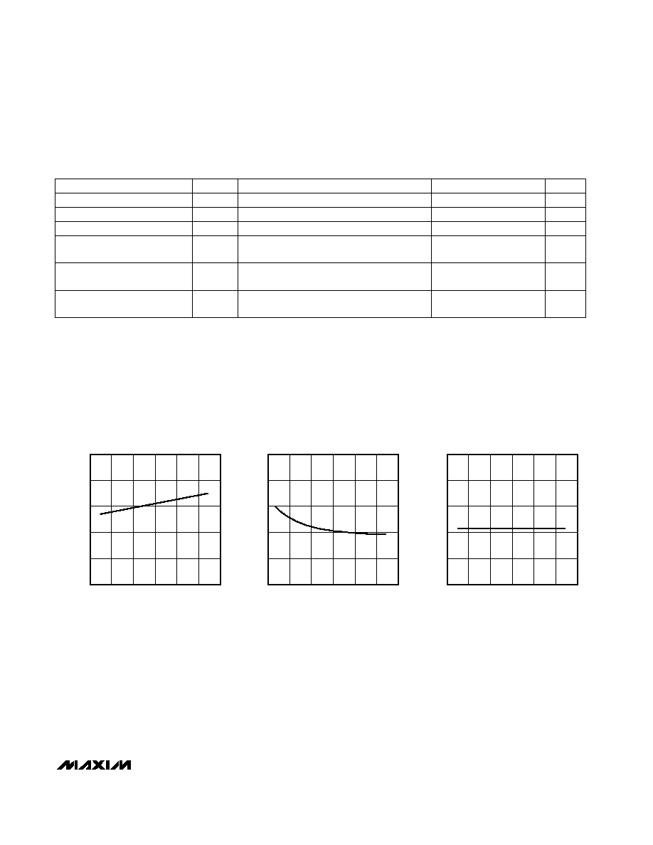
SUPPLY CURRENT
vs. TEMPERATURE
20
60
80
MAX3691-01
TEMPERATURE (∞C)
SUPPLY CURRENT (mA)
0
50
40
75
-20
-120
-50
-25
25
100
PARALLEL DATA-SETUP TIME
vs. TEMPERATURE
-100
-60
-40
MAX3691-02
TEMPERATURE (∞C)
PARALLEL DATA-SETUP TIME (ps)
0
50
-80
75
250
150
-50
-25
25
100
PARALLEL DATA-HOLD TIME
vs. TEMPERATURE
170
210
230
MAX3691-03
TEMPERATURE (∞C)
PARALLEL DATA-HOLD TIME (ps)
0
50
190
75
__________________________________________Typical Operating Characteristics
(V
CC
= +3.0V to +3.6V, differential LVDS loads = 100
, unless otherwise noted.)
MAX3691
+3.3V, 622Mbps, SDH/SONET 4:1 Serializer
with Clock Synthesis and LVDS Inputs
4
_______________________________________________________________________________________
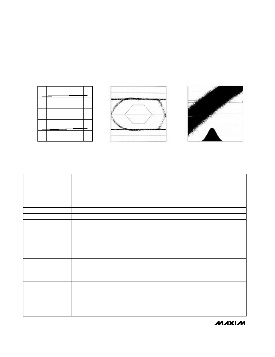
____________________________Typical Operating Characteristics (continued)
(V
CC
= +3.0V to +3.6V, differential LVDS loads = 100
, unless otherwise noted.)
6
-4
-50
-25
25
100
PCLKO-to-PCLKI SKEW
vs. TEMPERATURE
-2
2
4
MAX3691-04
TEMPERATURE (∞C)
PCLKO-TO-PCLKI SKEW (ns)
0
50
0
75
1.21V
0.59V
161ps/div
SERIAL-DATA OUTPUT EYE DIAGRAM
(622Mbps, 2
7
-1 PRBS)
62mV/
div
MAX3691-05
OC-12
SONET MASK
908mV
808mV
10ps/div
SERIAL-DATA OUTPUT JITTER
10mV/
div
MAX3691-06
f
RCLK
= 155.52MHz
Mean 23.88ns
RMS
8.418ps
PkPk 70.2ps
µ
±1
68.774%
µ
±2
95.534%
µ
±3
99.738%
______________________________________________________________Pin Description
NAME
FUNCTION
1, 3, 5, 7
PD0+ to PD3+
Noninverting LVDS Parallel Data Inputs. Data is clocked in on the PCLKI signal's positive transition.
2, 4, 6, 8
PD0- to PD3-
Inverting LVDS Parallel Data Inputs. Data is clocked in on the PCLKI signal's positive transition.
PIN
9, 17, 18,
19, 24,
25, 32
GND
Ground
10
PCLKO-
Inverting LVDS Parallel-Clock Output. Use PCLKO to clock the overhead management circuit.
15
SD+
Noninverting PECL Serial-Data Output
14
SD-
Inverting PECL Serial-Data Output
12, 13, 16,
20, 21,
28, 29
V
CC
+3.3V Supply Voltage
11
PCLKO+
Noninverting LVDS Parallel-Clock Output. Use PCLKO to clock the overhead management circuit.
23
FIL+
Filter Capacitor Input. See
Typical Operating Circuit for external-component connections.
22
FIL-
Filter Capacitor Input. See
Typical Operating Circuit for external-component connections.
26
RCLK+
Noninverting LVDS Reference Clock Input. Connect (AC couple) a crystal reference clock
(155.52MHz) to the RCLK inputs.
30
PCLKI+
Noninverting LVDS Parallel Clock Input. Connect the incoming parallel-data-clock signal to the
PCLKI inputs. Note that data is updated on the positive transition of the PCLKI signal.
27
RCLK-
Inverting LVDS Reference Clock Input. Connect (AC couple) a crystal reference clock (155.52MHz)
to the RCLK inputs.
31
PCLKI-
Inverting LVDS Parallel Clock Input. Connect the incoming parallel-data-clock signal to the PCLKI
inputs. Note that data is updated on the positive transition of the PCLKI signal.
MAX3691
+3.3V, 622Mbps, SDH/SONET 4:1 Serializer
with Clock Synthesis and LVDS Inputs
_______________________________________________________________________________________
5
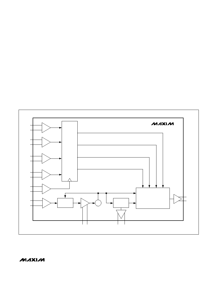
_______________Detailed Description
The MAX3691 serializer comprises a 4-bit parallel input
register, a 4-bit shift register, control and timing logic, a
PECL output buffer, LVDS input/output buffers, and a
frequency-synthesizing PLL (consisting of a phase/
frequency detector, loop filter/amplifier, and voltage-
controlled oscillator). This device converts 4-bit-wide,
155Mbps data to 622Mbps serial data (Figure 1).
The PLL synthesizes an internal 622Mbps reference
used to clock the output shift register. This clock is
generated by locking onto the external 155.52MHz
reference-clock signal (RCLK).
The incoming parallel data is clocked into the
MAX3691 on the rising transition of the parallel-clock-
input signal (PCLKI). The control and timing logic
ensure proper operation if the parallel-input register is
latched within a window of time that is defined with
respect to the parallel-clock-output signal (PCLKO).
PCLKO is the synthesized 622Mbps internal serial-
clock signal divided by four. The allowable PCLKO-to-
PCLKI skew is -0.7ns to +3.3ns. This defines a timing
window at about the PCLKO rising edge, during which
a PCLKI rising edge may occur. Figure 2 is the timing
diagram.
MAX3691
PD3+
PD3-
4-BIT
PARALLEL
INPUT
REGISTER
PHASE/FREQ
DETECT
CONTROL
4-BIT
SHIFT
REGISTER
LVDS
LVDS
PCLKI-
PCLKI+
RCLK-
RCLK+
FIL+ FIL-
PCLKO+ PCLKO-
VCO
PECL
SD+
SD-
SHIFT
LATCH
LVDS
PD2+
PD2-
LVDS
PD1+
PD1-
LVDS
PD0+
PD0-
LVDS
LVDS
Figure 1. Functional Diagram