 | –≠–ª–µ–∫—Ç—Ä–æ–Ω–Ω—ã–π –∫–æ–º–ø–æ–Ω–µ–Ω—Ç: MAX549 | –°–∫–∞—á–∞—Ç—å:  PDF PDF  ZIP ZIP |
_______________General Description
The MAX548A/MAX549A/MAX550A serial, 8-bit voltage-
output digital-to-analog converters (DACs) operate from
a single +2.5V to +5.5V supply. Their ±1LSB TUE spec-
ification is guaranteed over temperature. Operating cur-
rent (supply current plus reference current) is typically
75µA per DAC with V
DD
= 2.5V. In shutdown, the DAC
is disconnected from the reference, reducing current
drain to less than 1µA. The MAX548A/MAX549A allow
each DAC to be shut down independently.
The 10MHz, 3-wire serial interface is compatible with
SPITM/QSPITM and MicrowireTM interface standards.
Double-buffered inputs provide flexibility when updat-
ing the DACs; the input and DAC registers can be
updated individually or simultaneously.
The MAX548A is a dual DAC with an asynchronous
load input; it uses V
DD
as the reference input. The
MAX549A is a dual DAC with an external reference
input. The MAX550A is a single DAC with an external
reference input and an asynchronous load input.
The MAX548A/MAX549A/MAX550A's low power con-
sumption and small µMAX and DIP packages make
these devices ideal for portable and battery-powered
applications.
________________________Applications
Battery-Powered Systems
VCXO Control
Comparator-Level Settings
GaAs Amp Bias Control
Digital Gain and Offset Control
____________________________Features
o
+2.5V to +5.5V Single-Supply Operation
o
±1LSB (max) TUE
o
Power-On Reset Clears All Registers to Zero
o
Low Operating Current:
150µA (MAX548A/MAX549A, V
REF
= +2.5V)
75µA (MAX550A, V
REF
= +2.5V)
o
1µA Shutdown Mode
o
10MHz, 3-Wire Serial Interface Compatible with
SPI/QSPI and Microwire
o
µMAX Package--50% Smaller than 8-Pin SO
o
Independent Shutdown of DACs
(MAX548A/MAX549A)
MAX548A/MAX549A/MAX550A
+2.5V to +5.5V, Low-Power, Single/Dual,
8-Bit Voltage-Output DACs in µMAX Package
________________________________________________________________
Maxim Integrated Products
1
LDAC
SCLK
DIN
1
2
8
7
V
DD
OUTB
OUTA
CS
GND
DIP/
µ
MAX
TOP VIEW
3
4
6
5
MAX548A
_________________Pin Configurations
_____________________Selector Guide
19-1206; Rev 0; 3/97
PART
MAX548A
CPA
MAX548ACUA
MAX548AC/D
0∞C to +70∞C
0∞C to +70∞C
0∞C to +70∞C
TEMP. RANGE
PIN-PACKAGE
8 Plastic DIP
8 µMAX
Dice*
______________Ordering Information
Ordering Information continued at end of data sheet.
*
Dice are specified at T
A
= +25∞C, DC parameters only.
Contact factory for availability of 8-pin SO package.
For free samples & the latest literature: http://www.maxim-ic.com, or phone 1-800-998-8800
MAX548A
MAX549A
Number of DACs
2
2
DAC Reference
V
DD
External
FEATURE
External
Asynchronous
Load DAC Input
MAX550A
1
--
µMAX Package
SPI and QSPI are trademarks of Motorola Inc.
Microwire is a trademark of National Semiconductor Corp.
MAX548AEPA
MAX548AEUA
-40∞C to +85∞C
-40∞C to +85∞C
8 Plastic DIP
8 µMAX
Pin Configurations continued at end of data sheet.
MAX548A/MAX549A/MAX550A
+2.5V to +5.5V, Low-Power, Single/Dual,
8-Bit Voltage-Output DACs in µMAX Package
2
_______________________________________________________________________________________
ABSOLUTE MAXIMUM RATINGS
ELECTRICAL CHARACTERISTICS
(V
DD
= +2.5V to +5.5V, T
A
= T
MIN
to T
MAX
, unless otherwise noted. Typical values are at T
A
= +25∞C.)
Stresses beyond those listed under "Absolute Maximum Ratings" may cause permanent damage to the device. These are stress ratings only, and functional
operation of the device at these or any other conditions beyond those indicated in the operational sections of the specifications is not implied. Exposure to
absolute maximum rating conditions for extended periods may affect device reliability.
V
DD
, SCLK, DIN, CS, LDAC, OUT_ to GND ...............-0.3V to 6V
REF to GND ................................................-0.3V to (V
DD
+ 0.3V)
Maximum Current (any pin) .............................................±50mA
Continuous Power Dissipation (T
A
= +70∞C)
Plastic DIP (derate 9.09mW/∞C above +70∞C) .............727mW
µMAX (derate 4.10mW/∞C above +70∞C) .....................330mW
Operating Temperature Ranges
MAX5_ _AC_ A.....................................................0∞C to +70∞C
MAX5_ _AE_ A ..................................................-40∞C to +85∞C
Storage Temperature Range .............................-65∞C to +150∞C
Lead Temperature (soldering, 10sec) .............................+300∞C
MAX549A
MAX549A/MAX550A for specified
performance
Guaranteed
monotonic
CONDITIONS
16.7
V
2.5
V
DD
V
REF
Reference Input
Voltage Range
±0.9
Bits
8
N
Resolution
LSB
±0.9
DNL
Differential Nonlinearity
LSB
±1
ZCE
Zero-Code Error
LSB
±1
FSE
Full-Scale Error
UNITS
MIN
TYP
MAX
SYMBOL
PARAMETER
MAX5_ _AEUA (Note 1)
All others
MAX549A/MAX550A
MAX548A
MAX550A
k
33.3
R
OUT
DAC Output Resistance
V
0
V
REF
DAC Output Voltage Swing
0
V
DD
k
33.3
R
REF
Reference Input Resistance
DAC Code = 55 Hex (Note 2)
MAX548A/MAX549A
%
±0.2
R
OUT
/
R
OUT
DAC Output Resistance
Matching
±1
MAX5_ _AEUA (Note 1)
All others
LSB
±1
TUE
Total Unadjusted Error
MAX549A
330
550
150
250
MAX550A
165
275
µA
75
125
I
REF
Reference Input Current
DAC Code = 55 Hex (Note 3)
V
DD
= V
REF
= 5.5V
V
DD
= V
REF
= 2.5V
V
DD
= V
REF
= 5.5V
V
DD
= V
REF
= 2.5V
V
0.7V
DD
V
IH
Input High Voltage
V
0.3V
DD
V
IL
Input Low Voltage
V
IN
= 0V or V
DD
µA
±1
I
IN
Input Current
pF
10
C
IN
Input Capacitance (Note 4)
STATIC PERFORMANCE
REFERENCE INPUT
DAC OUTPUT
DIGITAL INPUTS
MAX548A/MAX549A/MAX550A
+2.5V to +5.5V, Low-Power, Single/Dual,
8-Bit Voltage-Output DACs in µMAX Package
_______________________________________________________________________________________
3
ELECTRICAL CHARACTERISTICS (continued)
(V
DD
= +2.5V to +5.5V, T
A
= T
MIN
to T
MAX
, unless otherwise noted. Typical values are at T
A
= +25∞C)
TIMING CHARACTERISTICS
(V
DD
= +2.5V to +5.5V, T
A
= T
MIN
to T
MAX
, unless otherwise noted. Digital inputs switching from 0V to V
DD
.) (Figure 3) (Note 4)
Note 1:
Cold temperature specifications (to -40∞C) guaranteed by design using six sigma design limits.
Note 2:
Worst-case input resistance at REF occurs at DAC code 55 hex.
Note 3:
Worst-case reference input current occurs at DAC code 55 hex.
Note 4:
Guaranteed by design. Not production tested.
Note 5:
I
DD
measured with DACs loaded with worst-case DAC code 55 hex.
CS = high, all digital inputs from 0V to V
DD
C
L
= 20pF
To ±1/2LSB, C
L
= 20pF
V/µs
3.1
µs
1.4
Voltage-Output Settling Time
4
CONDITIONS
50
nV-sec
Digital Feedthrough and
Crosstalk
UNITS
MIN
TYP
MAX
SYMBOL
PARAMETER
Voltage-Output Slew Rate
C
L
= 20pF
µs
Wake-Up Time at Power-Up
4
V
DD
= 2.5V
V
DD
= 5.5V
Supply Voltage Range
Outputs unloaded, all inputs = GND or V
DD
V
DD
V
2.5
5.5
Supply Current
(MAX549A/MAX550A)
Outputs unloaded,
all inputs = GND or
V
DD
(Note 5)
µA
330
550
I
DD
Supply Current (MAX548A)
Outputs unloaded, all inputs = GND or V
DD
;
V
DD
= 5.5V
I
DD
µA
0.3
10
V
DD
= 5.5V
V
DD
= 2.5V
Shutdown Current
Shutdown mode
µA
0.3
150
250
80
50
SCLK Period
t
CP
CS High to LDAC Low
ns
t
CSLD
ns
MAX548A/MAX550A only
5
V
DD
High to CS Low
µs
50
LDAC Pulse Width Low
t
LDAC
ns
MAX548A/MAX550A only
40
CS Pulse Width High
t
CSW
ns
20
t
CSH1
ns
V
DD
= 5.5V
10
30
t
DH
CS High to SCLK High Setup
ns
t
CSS1
ns
10
Delay, SCLK High to CS High
V
DD
= 2.5V
V
DD
= 5.5V
30
CS Low to SCLK High Setup
t
CSS0
ns
30
DIN to SCLK High Setup
t
DS
ns
0
DIN to SCLK High Hold
V
DD
= 2.5V
40
SCLK Pulse Width Low
t
CL
ns
PARAMETER
SYMBOL
MIN
TYP
MAX
UNITS
CONDITIONS
40
SCLK Pulse Width High
t
CH
ns
DYNAMIC PERFORMANCE
POWER SUPPLIES
10
SCLK High to CS Low Hold
t
CSH0
ns
MAX548A/MAX549A/MAX550A
+2.5V to +5.5V, Low-Power, Single/Dual,
8-Bit Voltage-Output DACs in µMAX Package
4
_______________________________________________________________________________________
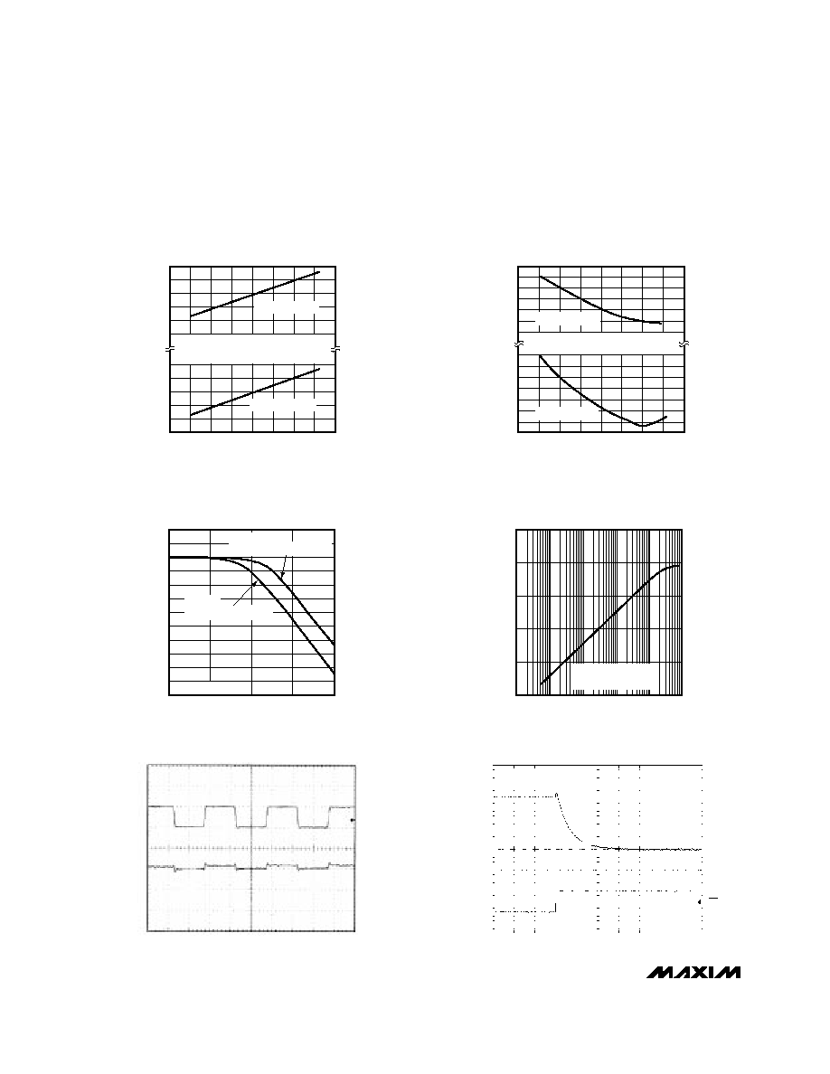
__________________________________________Typical Operating Characteristics
(V
DD
= V
REF
= 2.5V, R
L
= 1M
, C
L
= 15pF, T
A
= +25∞C, unless otherwise noted.)
-60
-20
20
100
OPERATING CURRENT PER DAC
vs. TEMPERATURE
75.0
74.6
149.8
150.2
MAX548A-550A TOC-01
TEMPERATURE (∞C)
OPERATING CURRENT PER DAC (
µ
A)
60
149.4
75.4
V
DD
= V
REF
= 5.0V
V
DD
= V
REF
= 2.5V
-60
-20
20
100
SHUTDOWN CURRENT
vs. TEMPERATURE
36
32
28
160
200
240
MAX548A-550A TOC-02
TEMPERATURE (∞C)
SHUTDOWN CURRENT (nA)
60
120
40
V
DD
= V
REF
= 5.0V
V
DD
= V
REF
= 2.5V
-50
1k
10k
100k
1M
10M
MAX549A/MAX550A
REFERENCE SMALL-SIGNAL
FREQUENCY RESPONSE
-40
10
0
MAX548A-550A TOC-03
FREQUENCY (Hz)
RELATIVE OUTPUT (dB)
-20
-30
-10
DAC CODE = FF hex
V
DD
= 5V
V
REF
= 2Vp-p SINE WAVE
V
DD
= 2.5V
V
REF
= 100mVp-p SINE WAVE
0
-100
10
1M
100k
10k
1k
100
MAX549A/MAX550A
REFERENCE AC FEEDTHROUGH
vs. FREQUENCY
-60
-80
MAX548A-550A TOC-04
FREQUENCY (Hz)
RELATIVE OUTPUT (dB)
-40
-20
V
REF
= 1Vp-p SINE WAVE
DAC CODE = 00 hex
DIGITAL FEEDTHROUGH
SCLK, 5V/div
OUT, 50mV/div
200ns/div
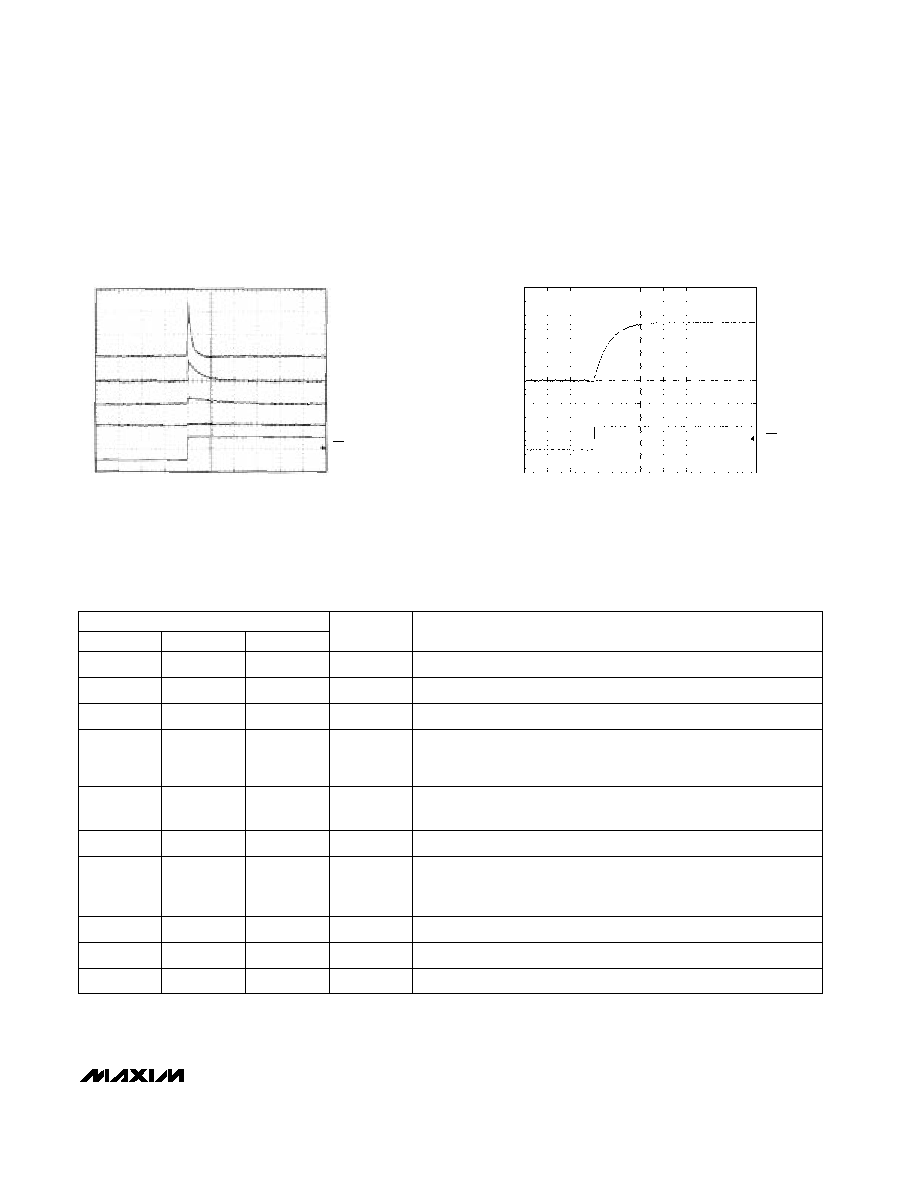
MAX548A-550A TOC-05
SETTLING TIME (FALLING)
OUT, 1V/div
2
µ
s/div
MAX548A-550A TOC-06
CS, 5V/div
DAC CODE FF hex to 00 hex
MAX548A/MAX549A/MAX550A
+2.5V to +5.5V, Low-Power, Single/Dual,
8-Bit Voltage-Output DACs in µMAX Package
_______________________________________________________________________________________
5
OUTPUT GLITCH FILTERING
OUT, 50mV/div, C
L
= 0pF
OUT, 50mV/div, C
L
= 100pF
OUT, 50mV/div, C
L
= 220pF
5
µ
s/div
OUT, 50mV/div, C
L
= 1000pF
MAX548A-550A TOC-07
CS, 5V/div
CODE = 00 hex
_____________________________Typical Operating Characteristics (continued)
(V
DD
= V
REF
= 2.5V, R
L
= 1M
, C
L
= 15pF, T
A
= +25∞C, unless otherwise noted.)
SETTLING TIME (RISING)
OUT, 1V/div
2
µ
s/div
MAX548A-550A TOC-08
CS, 5V/div
DAC CODE 00 hex to FF hex
______________________________________________________________Pin Description
Ground
1
1
1
GND
DAC A Output Voltage
2
2
--
OUTA
Chip-Select Input. A logic low on CS enables serial data to be
clocked into the input shift register. Programming commands are
executed at CS's rising edge.
3
3
3
CS
DAC Output Voltage
--
--
2
OUT
Serial-Clock Input. Data is clocked in on SCLK's rising edge.
5
5
5
SCLK
DAC B Output Voltage
6
7
--
OUTB
Load DAC Input. After CS goes high and if programmed by the
control word, a falling edge on LDAC updates the DAC latch(es).
Connect LDAC to V
DD
if unused.
--
6
6
LDAC
Serial-Data Input. Data is clocked into the 16-bit input shift register on
SCLK's rising edge.
4
4
4
DIN
Positive Power Supply (+2.5V to +5.5V)
8
8
8
V
DD
External Reference Voltage Input for DAC(s)
7
--
7
REF
MAX548A
MAX549A
MAX550A
NAME
FUNCTION
PIN