 | ÐлекÑÑоннÑй компоненÑ: MAX6126 | СкаÑаÑÑ:  PDF PDF  ZIP ZIP |
Äîêóìåíòàöèÿ è îïèñàíèÿ www.docs.chipfind.ru

General Description
The MAX6126 is an ultra-low-noise, high-precision, low-
dropout voltage reference. This family of voltage refer-
ences feature curvature-correction circuitry and
high-stability, laser-trimmed, thin-film resistors that
result in 3ppm/°C (max) temperature coefficients and
an excellent ±0.02% (max) initial accuracy. The propri-
etary low-noise reference architecture produces a low
flicker noise of 1.3µV
P-P
and wideband noise as low as
60nV/
Hz (2.048V output) without the increased supply
current usually found in low-noise references. Improve
wideband noise to 35nV/
Hz and AC power-supply
rejection by adding a 0.1µF capacitor at the noise
reduction pin. The MAX6126 series mode reference
operates from a wide 2.7V to 12.6V supply voltage
range and load-regulation specifications are guaran-
teed to be less than 0.025
for sink and source cur-
rents up to 10mA. These devices are available over the
automotive temperature range of -40°C to +125°C.
The MAX6126 typically draws 380µA of supply current
and is available in 2.048V, 2.500V, 3.000V, 4.096V, and
5.000V output voltages. These devices also feature
dropout voltages as low as 200mV. Unlike conventional
shunt-mode (two-terminal) references that waste supply
current and require an external resistor, the MAX6126
offers supply current that is virtually independent of
supply voltage and does not require an external resis-
tor. The MAX6126 is stable with 0.1µF to 10µF of load
capacitance.
The MAX6126 is available in the tiny 8-pin µMAX, as
well as 8-pin SO packages.
Applications
High-Resolution A/D and D/A Converters
ATE Equipment
High-Accuracy Reference Standard
Precision Current Sources
Digital Voltmeters
High-Accuracy Industrial and Process Control
Features
o Ultra-Low 1.3µV
P-P
Noise (0.1Hz to 10Hz, 2.048V
Output)
o Ultra-Low 3ppm/°C (max) Temperature Coefficient
o ±0.02% (max) Initial Accuracy
o Wide (V
OUT
+ 200mV) to 12.6V Supply Voltage
Range
o Low 200mV (max) Dropout Voltage
o 380µA Quiescent Supply Current
o 10mA Sink/Source-Current Capability
o Stable with C
LOAD
= 0.1µF to 10µF
o Low 20ppm/1000hr Long-Term Stability
o 0.025 (max) Load Regulation
o 20µV/V (max) Line Regulation
o Force and Sense Outputs for Remote Sensing
MAX6126
Ultra-High-Precision, Ultra-Low-Noise,
Series Voltage Reference
________________________________________________________________ Maxim Integrated Products
1
OUTS
I.C.*
GNDS
1
2
8
7
I.C.*
OUTF
IN
GND
NR
SO/
µMAX
TOP VIEW
3
4
6
5
MAX6126
*I.C. = INTERNALLY CONNECTED. DO NOT USE.
Pin Configuration
Ordering Information
19-2647; Rev 2; 6/03
For pricing, delivery, and ordering information, please contact Maxim/Dallas Direct! at
1-888-629-4642, or visit Maxim's website at www.maxim-ic.com.
PART
TEMP RANGE
PIN-
PACKAGE
OUTPUT
VOLTAGE
(V)
MAXIMUM INITIAL
ACCURACY (%)
MAXIMUM TEMPCO
(-40°C to +85°C)
(ppm/°C)
TOP
MARK
MAX6126AASA21
-40
°C to +125°C
8 SO
2.048
0.02
3
--
MAX6126BASA21
-40
°C to +125°C
8 SO
2.048
0.06
5
--
MAX6126AAUA21
-40
°C to +125°C
8 µMAX
2.048
0.06
3
6126A21
Ordering Information continued at end of data sheet.

MAX6126
Ultra-High-Precision, Ultra-Low-Noise,
Series Voltage Reference
2
_______________________________________________________________________________________
ABSOLUTE MAXIMUM RATINGS
Stresses beyond those listed under "Absolute Maximum Ratings" may cause permanent damage to the device. These are stress ratings only, and functional
operation of the device at these or any other conditions beyond those indicated in the operational sections of the specifications is not implied. Exposure to
absolute maximum rating conditions for extended periods may affect device reliability.
(All voltages referenced to GND)
GNDS ....................................................................-0.3V to +0.3V
IN ........................................................................... -0.3V to +13V
OUTF, OUTS, NR........ -0.3V to the lesser of (V
IN
+ 0.3V) or +6V
Output Short Circuit to GND or IN ..........................................60s
Continuous Power Dissipation (T
A
= +70°C)
8-Pin µMAX (derate 4.5mW/°C above +70°C) ............362mW
8-Pin SO (derate 5.88mW/°C above +70°C) ...............471mW
Operating Temperature Range ........................-40°C to +125°C
Junction Temperature .....................................................+150°C
Storage Temperature Range ............................-65°C to +150°C
Lead Temperature (soldering, 10s) ................................+300°C
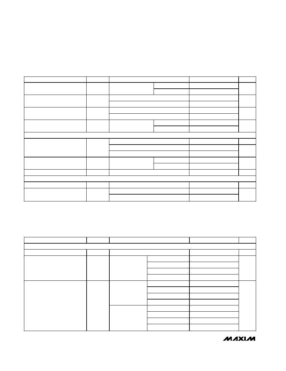
ELECTRICAL CHARACTERISTICS--MAX6126_21 (V
OUT
= 2.048V)
(V
IN
= 5V, C
LOAD
= 0.1µF, I
OUT
= 0, T
A
= T
MIN
to T
MAX
, unless otherwise noted. Typical values are at T
A
= +25°C.)
PARAMETER
SYMBOL
CONDITIONS
MIN
TYP
MAX
UNITS
OUTPUT
Output Voltage
V
OUT
T
A
= +25
°C
2.048
V
A grade SO
-0.02
+0.02
B grade SO
-0.06
+0.06
A grade µMAX
-0.06
+0.06
Output Voltage Accuracy
Referred to
V
OUT
,
T
A
= +25
°C
B grade µMAX
-0.1
+0.1
%
A grade SO
0.5
3
B grade SO
1
5
A grade µMAX
1
3
T
A
= -40
°C
to +85
°C
B grade µMAX
2
7
A grade SO
1
5
B grade SO
2
10
A grade µMAX
2
5
Output Voltage Temperature
Coefficient (Note 1)
TCV
OUT
T
A
= -40
°C
to +125
°C
B grade µMAX
3
12
ppm/
°C
T
A
= +25
°C
2
20
Line Regulation
V
OUT
/
V
IN
2.7V
V
IN
12.6V
T
A
= -40
°C to +125°C
40
µV/V
Sourcing: 0
I
OUT
10mA
0.7
25
Load Regulation
V
OUT
/
I
OUT
Sinking: -10mA
I
OUT
0
1.3
25
µV/mA
Short to GND
160
OUT Short-Circuit Current
I
SC
Short to IN
20
mA
SO
25
Thermal Hysteresis (Note 2)
V
OUT
/
cycle
µMAX
80
ppm
SO
20
Long-Term Stability
V
OUT
/
time
1000hr at T
A
= +25
°C
µMAX
100
ppm/
1000hr

MAX6126
Ultra-High-Precision, Ultra-Low-Noise,
Series Voltage Reference
_______________________________________________________________________________________
3
ELECTRICAL CHARACTERISTICS--MAX6126_21 (V
OUT
= 2.048V) (continued)
(V
IN
= 5V, C
LOAD
= 0.1µF, I
OUT
= 0, T
A
= T
MIN
to T
MAX
, unless otherwise noted. Typical values are at T
A
= +25°C.)
PARAMETER
SYMBOL
CONDITIONS
MIN
TYP
MAX
UNITS
DYNAMIC CHARACTERISTICS
f = 0.1Hz to 10Hz
1.3
µV
P-P
f = 1kHz, C
NR
= 0
60
Noise Voltage
e
OUT
f = 1kHz, C
NR
= 0.1µF
35
nV/
Hz
C
NR
= 0
0.8
Turn-On Settling Time
t
R
To V
OUT
= 0.01% of
final value
C
NR
= 0.1µF
20
ms
Capacitive-Load Stability Range
C
LOAD
No sustained oscillations
0.1 to 10
µF
INPUT
Supply Voltage Range
V
IN
Guaranteed by line-regulation test
2.7
12.6
V
T
A
= +25
°C
380
550
Quiescent Supply Current
I
IN
T
A
= -40
°C to +125°C
725
µA
ELECTRICAL CHARACTERISTICS--MAX6126_25 (V
OUT
= 2.500V)
(V
IN
= 5V, C
LOAD
= 0.1µF, I
OUT
= 0, T
A
= T
MIN
to T
MAX
, unless otherwise noted. Typical values are at T
A
= +25°C.)
PARAMETER
SYMBOL
CONDITIONS
MIN
TYP
MAX
UNITS
OUTPUT
Output Voltage
V
OUT
T
A
= +25
°C
2.500
V
A grade SO
-0.02
+0.02
B grade SO
-0.06
+0.06
A grade µMAX
-0.06
+0.06
Output Voltage Accuracy
Referred to V
OUT
,
T
A
= +25
°C
B grade µMAX
-0.1
+0.1
%
A grade SO
0.5
3
B grade SO
1
5
A grade µMAX
1
3
T
A
= -40
°C to +85°C
B grade µMAX
2
7
A grade SO
1
5
B grade SO
2
10
A grade µMAX
2
5
Output Voltage Temperature
Coefficient (Note 1)
TCV
OUT
T
A
= -40
°C to
+125
°C
B grade µMAX
3
12
ppm/
°C
T
A
= +25
°C
3
20
Line Regulation
V
OUT
/
V
IN
2.7V
V
IN
12.6V
T
A
= -40
°C to +125°C
40
µV/V
Sourcing: 0
I
OUT
10mA
1
25
Load Regulation
V
OUT
/
I
OUT
Sinking: -10mA
I
OUT
0
1.8
25
µV/mA
MAX6126
Ultra-High-Precision, Ultra-Low-Noise,
Series Voltage Reference
4
_______________________________________________________________________________________
PARAMETER
SYMBOL
CONDITIONS
MIN
TYP
MAX
UNITS
I
OUT
= 5mA
0.06
0.2
Dropout Voltage (Note 3)
V
IN
- V
OUT
V
OUT
= 0.1%
I
OUT
= 10mA
0.12
0.4
V
Short to GND
160
OUT Short-Circuit Current
I
SC
Short to IN
20
mA
SO
35
Thermal Hysteresis (Note 2)
V
OUT
/
cycle
µMAX
80
ppm
SO
20
Long-Term Stability
V
OUT
/
time
1000hr at T
A
= +25
°C
µMAX
100
ppm/
1000hr
DYNAMIC CHARACTERISTICS
f = 0.1Hz to 10Hz
1.45
µV
P-P
f = 1kHz, C
NR
= 0
75
Noise Voltage
e
OUT
f = 1kHz, C
NR
= 0.1µF
45
nV/
Hz
C
NR
= 0
1
Turn-On Settling Time
t
R
To V
OUT
= 0.01% of
final value
C
NR
= 0.1µF
20
ms
Capacitive-Load Stability Range
C
LOAD
No sustained oscillations
0.1 to 10
µF
INPUT
Supply Voltage Range
V
IN
Guaranteed by line-regulation test
2.7
12.6
V
T
A
= +25
°C
380
550
Quiescent Supply Current
I
IN
T
A
= -40
°C to +125°C
725
µA
ELECTRICAL CHARACTERISTICS--MAX6126_25 (V
OUT
= 2.500V) (continued)
(V
IN
= 5V, C
LOAD
= 0.1µF, I
OUT
= 0, T
A
= T
MIN
to T
MAX
, unless otherwise noted. Typical values are at T
A
= +25°C.)
PARAMETER
SYMBOL
CONDITIONS
MIN
TYP
MAX
UNITS
OUTPUT
Output Voltage
V
OUT
T
A
= +25
°C
3.000
V
A grade SO
-0.02
+0.02
B grade SO
-0.06
+0.06
A grade µMAX
-0.06
+0.06
Output Voltage Accuracy
Referred to V
OUT
,
T
A
= +25
°C
B grade µMAX
-0.1
+0.1
%
A grade SO
0.5
3
B grade SO
1
5
A grade µMAX
1
3
T
A
= -40
°C to
+85
°C
B grade µMAX
2
7
A grade SO
1
5
B grade SO
2
10
A grade µMAX
2
5
Output Voltage Temperature
Coefficient (Note 1)
TCV
OUT
T
A
= -40
°C to
+125
°C
B grade µMAX
3
12
ppm/
°C
ELECTRICAL CHARACTERISTICS--MAX6126_30 (V
OUT
= 3.000V)
(V
IN
= 5V, C
LOAD
= 0.1µF, I
OUT
= 0, T
A
= T
MIN
to T
MAX
, unless otherwise noted. Typical values are at T
A
= +25°C.)

MAX6126
Ultra-High-Precision, Ultra-Low-Noise,
Series Voltage Reference
_______________________________________________________________________________________
5
ELECTRICAL CHARACTERISTICS--MAX6126_30 (V
OUT
= 3.000V) (continued)
(V
IN
= 5V, C
LOAD
= 0.1µF, I
OUT
= 0, T
A
= T
MIN
to T
MAX
, unless otherwise noted. Typical values are at T
A
= +25°C.)
PARAMETER
SYMBOL
CONDITIONS
MIN
TYP
MAX
UNITS
T
A
= +25
°C
4
25
Line Regulation
V
OUT
/
V
IN
3.2V
V
IN
12.6V
T
A
= -40
°C to +125°C
50
µV/V
Sourcing: 0
I
OUT
10mA
1.5
30
Load Regulation
V
OUT
/
I
OUT
Sinking: -10mA
I
OUT
0
2.8
30
µV/mA
I
OUT
= 5mA
0.06
0.2
Dropout Voltage (Note 3)
V
IN
- V
OUT
V
OUT
= 0.1%
I
OUT
= 10mA
0.11
0.4
V
Short to GND
160
OUT Short-Circuit Current
I
SC
Short to IN
20
mA
SO
20
Thermal Hysteresis (Note 2)
V
OUT
/
cycle
µMAX
80
ppm
SO
20
Long-Term Stability
V
OUT
/
time
1000hr at T
A
= +25
°C
µMAX
100
ppm/
1000hr
DYNAMIC CHARACTERISTICS
f = 0.1Hz to 10Hz
1.75
µV
P-P
f = 1kHz, C
NR
= 0
90
Noise Voltage
e
OUT
f = 1kHz, C
NR
= 0.1µF
55
nV/
Hz
Capacitive-Load Stability Range
C
LOAD
No sustained oscillations
0.1 to 10
µF
C
NR
= 0
1.2
Turn-On Settling Time
t
R
To V
OUT
= 0.01%
of final value
C
NR
= 0.1µF
20
ms
INPUT
Supply Voltage Range
V
IN
Guaranteed by line-regulation test
3.2
12.6
V
T
A
= +25
°C
380
550
Quiescent Supply Current
I
IN
T
A
= -40
°C to +125°C
725
µA
ELECTRICAL CHARACTERISTICS--MAX6126_41 (V
OUT
= 4.096V)
(V
IN
= 5V, C
LOAD
= 0.1µF, I
OUT
= 0, T
A
= T
MIN
to T
MAX
, unless otherwise noted. Typical values are at T
A
= +25°C.)
PARAMETER
SYMBOL
CONDITIONS
MIN
TYP
MAX
UNITS
OUTPUT
Output Voltage
V
OUT
T
A
= +25
°C
4.096
V
A grade SO
-0.02
+0.02
B grade SO
-0.06
+0.06
A grade µMAX
-0.06
+0.06
Output Voltage Accuracy
Referred to V
OUT
,
T
A
= +25
°C
B grade µMAX
-0.1
+0.1
%