General Description
The MAX6746≠MAX6753 low-power microprocessor
(µP) supervisory circuits monitor single/dual system
supply voltages from 1.575V to 5V and provide maxi-
mum adjustability for reset and watchdog functions.
These devices assert a reset signal whenever the V
CC
supply voltage or RESET IN falls below its reset thresh-
old or when manual reset is pulled low. The reset output
remains asserted for the reset timeout period after V
CC
and RESET IN rise above the reset threshold. The reset
function features immunity to power-supply transients.
The MAX6746≠MAX6753 have ±2% factory-trimmed
reset threshold voltages in approximately 100mV incre-
ments from 1.575V to 5.0V and/or adjustable reset
threshold voltages using external resistors.
The reset and watchdog delays are adjustable with
external capacitors. The MAX6746≠MAX6751 contain a
watchdog select input that extends the watchdog time-
out period by 128x. The MAX6752/MAX6753 contain a
window watchdog timer that looks for activity outside an
expected window of operation.
The MAX6746≠MAX6753 are available with a push-pull
or open-drain active-low RESET output. The MAX6746≠
MAX6753 are available in an 8-pin SOT23 package and
are fully specified over the automotive temperature
range (-40∞C to +125∞C).
Applications
Features
o Factory-Set Reset Threshold Options from 1.575V
to 5V in ~100mV Increments
o Adjustable Reset Threshold Options
o Single/Dual Voltage Monitoring
o Capacitor-Adjustable Reset Timeout
o Capacitor-Adjustable Watchdog Timeout
o Min/Max (Windowed) Watchdog Option
o Manual Reset Input Option
o Guaranteed RESET Valid for V
CC
1V
o 3.7µA Supply Current
o Push-Pull or Open-Drain RESET Output Options
o Power-Supply Transient Immunity
o Small 8-Pin SOT23 Packages
MAX6746≠MAX6753
µP Reset Circuits with Capacitor-Adjustable
Reset/Watchdog Timeout Delay
________________________________________________________________ Maxim Integrated Products
1
WDI
WDS
GND
1
2
8
7
V
CC
RESET
SWT
SRT
RESET IN (MR)
( ) ARE FOR MAX6746 AND MAX6747 ONLY.
TOP VIEW
3
4
6
5
MAX6746≠
MAX6751
SOT23-8
Pin Configurations
19-2530; Rev 1; 1/03
For pricing, delivery, and ordering information, please contact Maxim/Dallas Direct! at
1-888-629-4642, or visit Maxim's website at www.maxim-ic.com.
Note: "_ _" represents the two number suffix needed when
ordering the reset threshold voltage value for the
MAX6746/MAX6747 and MAX6750≠MAX6753. The reset
threshold voltages are available in approximately 100mV incre-
ments. Table 2 contains the suffix and reset factory-trimmed
voltages. All devices are available in tape-and-reel only. There
is a 2500-piece minimum order increment for standard ver-
sions (see Table 3). Sample stock is typically held on standard
versions only. Nonstandard versions require a minimum order
increment of 10,000 pieces. Contact factory for availability.
Medical Equipment
Automotive
Intelligent Instruments
Portable Equipment
Battery-Powered
Computers/Controllers
Embedded Controllers
Critical µP Monitoring
Set-Top Boxes
Computers
Ordering Information
PART
TEMP RANGE
PIN-PACKAGE
MAX6746KA_ _-T
-40∞C to +125∞C
8 SOT23-8
MAX6747KA_ _-T
-40∞C to +125∞C
8 SOT23-8
MAX6748KA-T
-40∞C to +125∞C
8 SOT23-8
MAX6749KA-T
-40∞C to +125∞C
8 SOT23-8
MAX6750KA_ _-T
-40∞C to +125∞C
8 SOT23-8
MAX6751KA_ _-T
-40∞C to +125∞C
8 SOT23-8
MAX6752KA_ _-T
-40∞C to +125∞C
8 SOT23-8
MAX6753KA_ _-T
-40∞C to +125∞C
8 SOT23-8
Selector Guide appears at end of data sheet.
Typical Operating Circuit appears at end of data sheet.
Pin Configurations continued at end of data sheet.
MAX6746≠MAX6753
µP Reset Circuits with Capacitor-Adjustable
Reset/Watchdog Timeout Delay
2
_______________________________________________________________________________________
ABSOLUTE MAXIMUM RATINGS
ELECTRICAL CHARACTERISTICS
(V
CC
= +1.2V to +5.5V, T
A
= T
MIN
to T
MAX
, unless otherwise specified. Typical values are at V
CC
= +5V and T
A
= +25∞C.) (Note 1)
Stresses beyond those listed under "Absolute Maximum Ratings" may cause permanent damage to the device. These are stress ratings only, and functional
operation of the device at these or any other conditions beyond those indicated in the operational sections of the specifications is not implied. Exposure to
absolute maximum rating conditions for extended periods may affect device reliability.
V
CC
to GND ...........................................................-0.3V to +6.0V
SRT, SWT, SET0, SET1, RESET IN, WDS, MR,
WDI, to GND ..........................................-0.3V to (V
CC
+ 0.3V)
RESET (Push-Pull) to GND.........................-0.3V to (V
CC
+ 0.3V)
RESET (Open Drain) to GND ................................-0.3V to +6.0V
Input Current (All Pins) .....................................................±20mA
Output Current (RESET) ...................................................±20mA
Continuous Power Dissipation (T
A
= +70∞C)
8-Pin SOT23 (derate 8.9mW/∞C above +70∞C)............714mW
Operating Temperature Range .........................-40∞C to +125∞C
Storage Temperature Range ............................-65∞C to +150∞C
Junction Temperature ......................................................+150∞C
Lead Temperature (soldering, 10s) .................................+300∞C
PARAMETER
SYMBOL
CONDITIONS
MIN
TYP
MAX
UNITS
T
A
= 0∞C to +125∞C
1.0
5.5
Supply Voltage
V
CC
T
A
= -40∞C to 0∞C
1.2
5.5
V
V
CC
5.5V
5
10
V
CC
3.3V
4.2
9
Supply Current
I
CC
V
CC
2.0V
3.7
8
µA
V
CC
Reset Threshold
V
TH
See V
TH
selection table
TA = -40∞C to+125∞C
V
TH
-
2%
V
TH
+
2%
V
Hysteresis
V
HYST
0.8
%
V
CC
to Reset Delay
V
CC
falling from V
TH
+ 100mV to V
TH
-
100mV at 1mV/µs
20
µs
C
SRT
= 1500pF
5.692
7.590
9.487
Reset Timeout Period
t
RP
C
SRT
= 100pF
0.506
ms
SRT
Ramp Current
I
RAMP
V
SRT
= 0 to 1.23V; V
CC
= 1.6V to 5V
200
250
300
nA
SRT
Ramp Threshold
V
RAMP
V
CC
= 1.6V to 5V (V
RAMP
rising)
1.173
1.235
1.297
V
C
SWT
= 1500pF
5.692
7.590
9.487
Normal Watchdog Timeout Period
(MAX6746≠MAX6751)
t
WD
C
SWT
= 100pF
0.506
ms
C
SWT
= 1500pF
728.6
971.5
1214.4
Extended Watchdog Timeout
(MAX6746≠MAX6751)
t
WD
C
SWT
= 100pF
64.77
ms
C
SWT
= 1500pF
728.6
971.5
1214.4
Slow Watchdog Period
(MAX6752/MAX6753)
t
WD2
C
SWT
= 100pF
64.77
ms
C
SWT
= 1500pF
91.08
121.43
151.80
Fast Watchdog Timeout Period,
SET Ratio = 8,
(MAX6752/MAX6753)
t
WD1
C
SWT
= 100pF
8.09
ms
C
SWT
= 1500pF
45.53
60.71
75.89
Fast Watchdog Timeout Period,
SET Ratio = 16,
(MAX6752/MAX6753)
t
WD1
C
SWT
= 100pF
4.05
ms
MAX6746≠MAX6753
µP Reset Circuits with Capacitor-Adjustable
Reset/Watchdog Timeout Delay
_______________________________________________________________________________________
3
ELECTRICAL CHARACTERISTICS (continued)
(V
CC
= +1.2V to +5.5V, T
A
= T
MIN
to T
MAX
, unless otherwise specified. Typical values are at V
CC
= +5V and T
A
= +25∞C.) (Note 1)
PARAMETER
SYMBOL
CONDITIONS
MIN
TYP
MAX
UNITS
C
SWT
= 1500pF
11.38
15.18
18.98
Fast Watchdog Timeout Period,
SET Ratio = 64,
(MAX6752/MAX6753)
t
WD1
C
SWT
= 100pF
1.01
ms
Fast Watchdog Minimum Period
(MAX6752/MAX6753)
2000
ns
SWT
Ramp Current
I
RAMP
V
SWT
= 0 to 1.23V, V
CC
= 1.6V to 5V
200
250
300
nA
SWT
Ramp Threshold
V
RAMP
V
CC
= 1.6V to 5V (V
RAMP
rising)
1.173
1.235
1.297
V
V
CC
1.0V, I
SINK
= 50µA
0.3
V
CC
2.7V, I
SINK
= 1.2mA
0.3
RESET Output Voltage LOW
Open-Drain, Push-Pull
(Asserted)
V
OL
V
CC
4.5V, I
SINK
= 3.2mA
0.4
V
V
CC
1.8V, I
SOURCE
= 200µA
0.8 x V
CC
V
CC
2.25V, I
SOURCE
= 500µA
0.8 x V
CC
RESET Output Voltage HIGH,
Push-Pull (Not Asserted)
V
OH
V
CC
4.5V, I
SOURCE
= 800µA
0.8 x V
CC
V
RESET Output Leakage Current,
Open Drain
I
LKG
V
CC
> V
TH
, reset not asserted,
V
RESET
= 5.5V
1.0
µA
DIGITAL INPUTS (MR, SET0, SET1, WDI, WDS)
V
IL
0.8
V
IH
V
CC
4.0V
2.4
V
IL
V
CC
< 4.0V
0.3 x V
CC
Input Logic Levels
V
IH
0.7 x V
CC
V
MR Minimum Pulse Width
1
µs
MR Glitch Rejection
100
ns
MR to RESET Delay
200
ns
MR Pullup Resistance
Pullup to V
CC
12
20
28
k
WDI Minimum Pulse Width
300
ns
RESET IN
RESET IN Threshold
V
RESET IN
TA = -40∞C to +125∞C
1.216
1.235
1.254
V
RESET IN Leakage Current
I
RESET IN
-50
±1
+50
nA
RESET IN to RESET Delay
RESET IN falling at 1mV/µs
20
µs
Note 1: Production testing done at T
A
= +25∞C. Over temperature limits are guaranteed by design.
MAX6746≠MAX6753
µP Reset Circuits with Capacitor-Adjustable
Reset/Watchdog Timeout Delay
4
_______________________________________________________________________________________
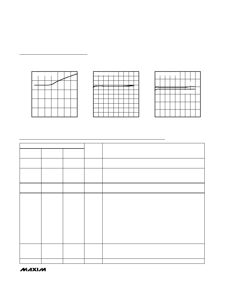
Typical Operating Characteristics
(V
CC
= +5V, T
A
= +25∞C, unless otherwise noted.)
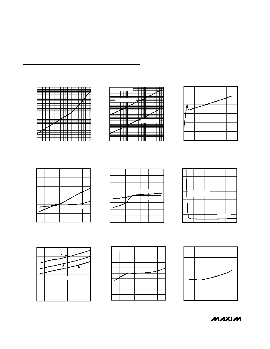
RESET TIMEOUT PERIOD vs. C
SRT
MAX6746 toc01
C
SRT
(pF)
RESET TIMEOUT PERIOD (ms)
10,000
1000
1
10
100
1000
10,000
0.1
100
100,000
WATCHDOG TIMEOUT PERIOD vs. C
SWT
MAX6746 toc02
C
SWT
(pF)
WATCHDOG TIMEOUT PERIOD (ms)
10,000
1000
1
10
100
1000
10,000
100,000
0.1
100
100,000
MAX6746≠MAX6751
EXTENDED MODE
NORMAL MODE
SUPPLY CURRENT
vs. SUPPLY VOLTAGE
MAX6746 toc03
SUPPLY VOLTAGE (V)
SUPPLY CURRENT (
µ
A)
5
4
3
2
2
1
3
4
5
6
0
1
6
NORMALIZED RESET TIMEOUT PERIOD
vs. TEMPERATURE
MAX6746 toc04
TEMPERATURE (
∞C)
NORMALIZED TIMEOUT PERIOD
100
75
50
25
0
-25
0.95
1.00
1.05
1.10
1.15
1.20
0.90
-50
125
C
SRT
= 100pF
C
SRT
= 1500pF
NORMALIZED WATCHDOG TIMEOUT PERIOD
vs. TEMPERATURE
MAX6746 toc05
TEMPERATURE (
∞C)
NORMALIZED TIMEOUT PERIOD
100
75
50
25
0
-25
0.95
0.90
0.85
1.00
1.05
1.10
1.15
1.20
0.80
-50
125
C
SWT
= 100pF
C
SWT
= 1500pF
MAXIMUM TRANSIENT DURATION
vs. RESET THRESHOLD OVERDRIVE
MAX6746 toc06
RESET THRESHOLD OVERDRIVE (mV)
TRANSIENT DURATION (
µ
s)
800
600
400
200
25
50
75
100
125
150
175
0
0
1000
RESET OCCURS
ABOVE THE CURVE
V
TH
= 2.92V
SUPPLY CURRENT
vs. TEMPERATURE
MAX6746 toc07
TEMPERATURE (
∞C)
SUPPLY CURRENT (
µ
A)
100
75
25
50
0
-25
1
2
3
4
5
6
0
-50
125
V
CC
= 3.3V
V
CC
= 1.8V
V
CC
= 5V
NORMALIZED RESET IN THRESHOLD VOLTAGE
vs. TEMPERATURE
MAX6746 toc08
TEMPERATURE (
∞C)
NORMALIZED RESET THRESHOLD VOLTAGE
100
75
50
25
0
-25
0.994
0.992
0.996
1.000
0.998
1.004
1.002
1.008
1.006
1.010
0.990
-50
125
V
CC
= 5V
RESET IN THRESHOLD
vs. SUPPLY VOLTAGE
MAX6746 toc08b
SUPPLY VOLTAGE (V)
RESET IN THRESHOLD (V)
5
4
3
2
1.236
1.237
1.238
1.239
1.240
1.235
1
6
MAX6746≠MAX6753
µP Reset Circuits with Capacitor-Adjustable
Reset/Watchdog Timeout Delay
_______________________________________________________________________________________
5
V
CC
TO RESET DELAY
vs. TEMPERATURE (V
CC
FALLING)
MAX6746 toc09
TEMPERATURE (
∞C)
V
CC
TO RESET DELAY (
µ
s)
100
75
50
25
0
-25
25.4
25.8
26.2
26.6
27.0
25.0
-50
125
V
CC
FALLING AT 1mV/
µs
RESET AND WATCHDOG
TIMEOUT PERIOD vs. V
CC
MAX6746 toc10
V
CC
(V)
TIMEOUT PERIOD (ms)
5.5
5.0
4.0 4.5
2.5 3.0 3.5
2.0
0.44
0.48
0.52
0.56
0.60
0.40
1.5
6.0
C
SWT
= C
SRT
= 100pF
Typical Operating Characteristics (continued)
(V
CC
= +5V, T
A
= +25∞C, unless otherwise noted.)
RESET AND WATCHING TIMEOUT
PERIOD vs. V
CC
MAX6746 toc11
V
CC
(V)
TIMEOUT PERIOD (ms)
5.5
5.0
4.5
4.0
3.5
3.0
2.5
2.0
6.5
7.0
7.5
8.0
8.5
9.0
6.0
1.5
6.0
C
SWT
= C
SRT
= 1500pF
RESET
WATCHDOG
Pin Description
PIN
MAX6746
MAX6747
MAX6748≠
MAX6751
MAX6752
MAX6753
NAME
FUNCTION
1
--
--
MR
Manual Reset Input. Pull MR low to manually reset the device. Reset
remains asserted for the reset timeout period after MR is released.
--
1
--
RESET IN
Reset Input. High-impedance input to the adjustable reset comparator.
Connect RESET IN to the center point of an external resistor-divider to
set the threshold of the externally monitored voltage.
--
--
1
SET0
Logic Input. SET0 selects watchdog window ratio or disables the
watchdog timer. See Table 1.
2
2
2
SWT
Watchdog Timeout Input.
MAX6746≠MAX6751: Connect a capacitor between SWT and ground to
set the basic watchdog timeout period (t
WD
). Determine the period by
the formula t
WD
= 5.06 x 10
6
x C
SWT
with t
WD
in seconds and C
SWT
in
Farads. Extend the basic watchdog timeout period by using the WDS
input.
MAX6752/MAX6753: Connect a capacitor between SWT and ground to
set the slow watchdog timeout period (t
WD2
). Determine the slow
watchdog period by the formula: t
WD2
= 0.65 x 10
9
x C
SWT
with t
WD2
in
seconds and C
SWT
in
Farads. The fast watchdog timeout period is set
by pinstrapping SET0 and SET1. See Table 1.
3
3
3
SRT
Reset Timeout Input. Connect a capacitor from SRT to GND to select
the reset timeout period. Determine the period as follows: t
RP
= 5.06 x
10
6
x C
SRT
with t
RP
in seconds and C
SRT
in
Farads.
4
4
4
GND
Ground