 | –≠–ª–µ–∫—Ç—Ä–æ–Ω–Ω—ã–π –∫–æ–º–ø–æ–Ω–µ–Ω—Ç: MAX681E | –°–∫–∞—á–∞—Ç—å:  PDF PDF  ZIP ZIP |
________________General Description
The MAX680/MAX681 are monolithic, CMOS, dual
charge-pump voltage converters that provide ±10V out-
puts from a +5V input voltage. The MAX680/MAX681 pro-
vide both a positive step-up charge pump to develop
+10V from +5V input and an inverting charge pump to
generate the -10V output. Both parts have an on-chip,
8kHz oscillator. The MAX681 has the capacitors internal to
the package, and the MAX680 requires four external
capacitors to produce both positive and negative voltages
from a single supply.
The output source impedances are typically 150
, pro-
viding useful output currents up to 10mA. The low quies-
cent current and high efficiency make this device suitable
for a variety of applications that need both positive and
negative voltages generated from a single supply.
The MAX864/MAX865 are also recommended for new
designs. The MAX864 operates at up to 200kHz and uses
smaller capacitors. The MAX865 comes in the smaller
µMAX package.
________________________Applications
The MAX680/MAX681 can be used wherever a single
positive supply is available and where positive and nega-
tive voltages are required. Common applications include
generating ±6V from a 3V battery and generating ±10V
from the standard +5V logic supply (for use with analog
circuitry). Typical applications include:
____________________________Features
o
95% Voltage-Conversion Efficiency
o
85% Power-Conversion Efficiency
o
+2V to +6V Voltage Range
o
Only Four External Capacitors Required (MAX680)
o
No Capacitors Required (MAX681)
o
500µA Supply Current
o
Monolithic CMOS Design
MAX680/MAX681
+5V to ±10V Voltage Converters
________________________________________________________________
Maxim Integrated Products
1
V
CC
C2-
GND
V-
1
2
8
7
V+
C1+
C2+
C1-
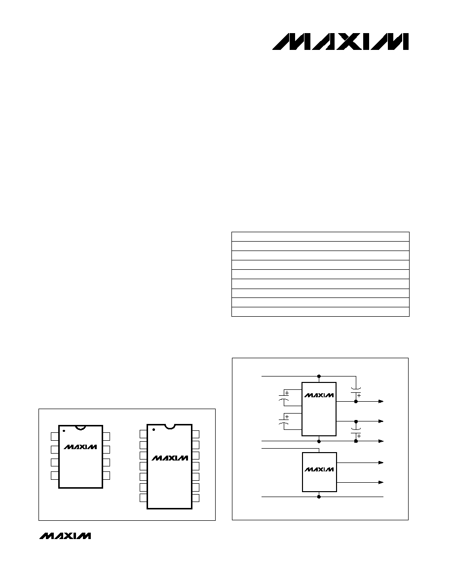
MAX680
DIP/SO
TOP VIEW
3
4
6
5
14
13
12
11
10
9
8
1
2
3
4
5
6
7
V
CC
V
CC
V
CC
V
CC
C2+
C1-
C1-
V+
MAX681
V+
GND
GND
V-
C2-
C2-
DIP
_________Typical Operating Circuits
MAX680
+10V
4.7
µ
F
4.7
µ
F
4.7
µ
F
4.7
µ
F
-10V
GND
+10V
-10V
GND
FOUR PINS REQUIRED
(MAX681 ONLY)
+5V
GND
GND
+5V
C1-
C1+
V-
V+
C2-
V
CC
GND
+5V to ±10V CONVERTER
MAX681
V-
V+
V
CC
GND
C1+
_________________Pin Configurations
19-0896; Rev 1; 7/96
PART
MAX680
CPA
MAX680CSA
MAX680C/D
0∞C to +70∞C
0∞C to +70∞C
0∞C to +70∞C
TEMP. RANGE
PIN-PACKAGE
8 Plastic DIP
8 Narrow SO
Dice
_______________Ordering Information
For free samples & the latest literature: http://www.maxim-ic.com, or phone 1-800-998-8800
MAX680EPA
MAX680ESA
-40∞C to +85∞C
-40∞C to +85∞C
8 Plastic DIP
8 Narrow SO
MAX680MJA
-55∞C to +125∞C
8 CERDIP
MAX681
CPD
MAX681EPD
-40∞C to +85∞C
0∞C to +70∞C
14 Plastic DIP
14 Plastic DIP
±6V from 3V Lithium Cell
Hand-Held Instruments
Data-Acquisition Systems
Panel Meters
±10V from +5V Logic
Supply
Battery-Operated
Equipment
Operational Amplifier
Power Supplies
MAX680/MAX681
+5V to ±10V Voltage Converters
2
_______________________________________________________________________________________
ABSOLUTE MAXIMUM RATINGS
ELECTRICAL CHARACTERISTICS
(V
CC
= +5V, test circuit Figure 1, T
A
= +25∞C, unless otherwise noted.)
Stresses beyond those listed under "Absolute Maximum Ratings" may cause permanent damage to the device. These are stress ratings only, and functional
operation of the device at these or any other conditions beyond those indicated in the operational sections of the specifications is not implied. Exposure to
absolute maximum rating conditions for extended periods may affect device reliability.
V
CC
................................................................................... +6.2V
V+ ...................................................................................... +12V
V- ..........................................................................................-12V
V- Short-Circuit Duration ...........................................Continuous
V+ Current ..........................................................................75mA
V
CC
V/
T ..........................................................................1V/µs
Continuous Power Dissipation (T
A
= +70∞C)
8-Pin Plastic DIP (derate 9.09mW/∞C above +70∞C) . ....727mW
8-Pin Narrow SO (derate 5.88mW/∞C above +70∞C) .....471mW
8-Pin CERDIP (derate 8.00mW/∞C above +70∞C) ..........640mW
14-Pin Plastic DIP (derate 10.00mW/∞C above +70∞C) ...800mW
Storage Temperature Range .............................-65∞C to +160∞C
Lead Temperature (soldering, 10sec) .............................+300∞C
kHz
4
8
Oscillator Frequency
Positive Charge-Pump
Output Source Resistance
2.5
1
2
0.5
1
400
350
180
300
3
3
Supply Current
mA
2.0
1.5 to 6.0
6.0
Supply-Voltage Range
150
250
MIN
TYP
MAX
V
CC
= 5V, 0∞C
T
A
+70∞C, R
L
=
V
CC
= 3V, T
A
= +25∞C, R
L
=
V
CC
= 5V, T
A
= +25∞C, R
L
=
I
L
+ = 10mA,
I
L
- = 0mA,
V
CC
= 5V
I
L
+ = 5mA, I
L
- = 0mA, V
CC
= 2.8V,
T
A
= +25∞C
V
CC
= 5V, -40∞C
T
A
+85∞C, R
L
=
V
CC
= 5V, -55∞C
T
A
+125∞C, R
L
=
MIN
T
A
MAX, R
L
= 10k
I
L
+ = 10mA, I
L
- = 0mA, V
CC
= 5V,
T
A
= +25∞C
CONDITIONS
UNITS
PARAMETER
V+, R
L
=
R
L
= 10k
95
99
%
85
Power Efficiency
I
L
- = 10mA,
I
L
+ = 0mA,
V+ = 10V
I
L
- = 5mA, I
L
+ = 0mA, V+ = 5.6V,
T
A
= +25∞C
I
L
- = 10mA, I
L
+ = 0mA, V+ = 10V,
T
A
= +25∞C
Negative Charge-Pump
Output Source Resistance
250
200
110
175
90
150
V-, R
L
=
%
90
97
Voltage-Conversion
Efficiency
V
325
200
0∞C
T
A
+70∞C
-40∞C
T
A
+85∞C
-55∞C
T
A
+125∞C
0∞C
T
A
+70∞C
-40∞C
T
A
+85∞C
-55∞C
T
A
+125∞C
MAX680/MAX681
+5V to ±10V Voltage Converters
_______________________________________________________________________________________
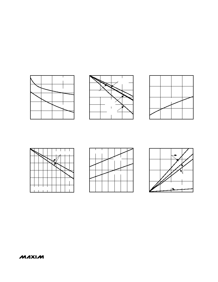
3
0
2.0
OUTPUT RESISTANCE
vs. SUPPLY VOLTAGE
MAX680/681-TOC1
V
(V)
OUTPUT RESISTANCE (
)
50
100
150
200
250
3.0
4.0
5.0
6.0
R
OUT
-
R
OUT
+
C1-C4 = 10
µ
F
4
0
OUTPUT VOLTAGE
vs. LOAD CURRENT
MAX680/681-TOC2
LOAD CURRENT ( A)
|
VOUT
|
(V)
5
6
7
8
9
10
5
10
15
20
V+ vs. I
L
+
I
L
- = 0
V- vs. I
L
+
I
L
- = 0
V+ vs. I
L
-
I
L
+ = 0
V- vs. I
L
-
I
L
+ = 0
0
2.0
SUPPLY CURRENT
vs. SUPPLY VOLTAGE
MAX680/681-TOC3
V
(V)
SUPPLY CURRENT (mA) 0.5
1.0
1.5
2.0
3.0
4.0
5.0
6.0
R
L
=
4
0
1
2
3
4
6
7
8
9
OUTPUT VOLTAGE vs. OUTPUT CURRENT
(FROM V+ TO V-)
MAX680/681-TOC4
OUTPUT CURRENT (mA)
|
VOUT
|
(V)
5
6
7
8
9
10
5
10
C1≠C4 = 10
µ
F
V-
V+
MAX680, MAX681
0
-50
OUTPUT SOURCE RESISTANCE
vs. TEMPERATURE
MAX680/681-TOC5
TEMPERATURE (∞C)
OUTPUT SOURCE RESISTANCE (
)
50
100
150
200
-25
0
25
50
75
100
125
R
OUT
+
R
OUT
-
V
CC
= 5V
0
OUTPUT RIPPLE vs.
OUTPUT CURRENT (I
L
+ OR I
L
-)
MAX681/681-TOC6
OUTPUT CURRENT (mA)
OUTPUT RIPPLE (mVp-p)
50
100
150
200
5
10
15
20
V+ AND V-
V-
V-
MAX681
V
CC
= 5V
V+
MAX680
C3, C4 = 100
µ
F
MAX680
C3, C4 = 10
µ
F
0
V+
__________________________________________Typical Operating Characteristics
(T
A
= +25∞C, unless otherwise noted.)
MAX680/MAX681
+5V to ±10V Voltage Converters
4
_______________________________________________________________________________________
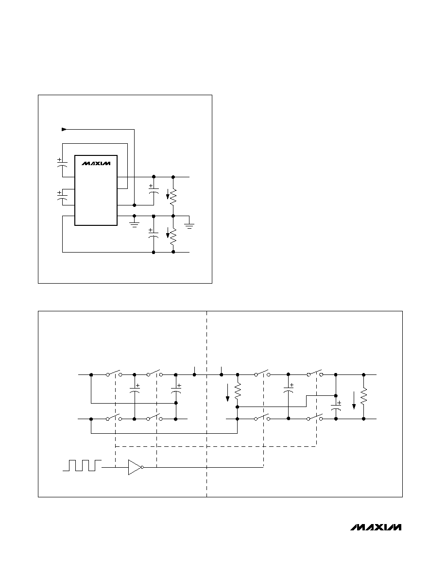
_______________Detailed Description
The MAX681 contains all circuitry needed to implement
a dual charge pump. The MAX680 needs only four
capacitors. These may be inexpensive electrolytic
capacitors with values in the 1µF to 100µF range. The
MAX681 contains two 1.5µF capacitors as C1 and C2,
and two 2.2µF capacitors as C3 and C4. See
Typical
Operating Characteristics.
Figure 2a shows the idealized operation of the positive
voltage converter. The on-chip oscillator generates a
50% duty-cycle clock signal. During the first half of the
cycle, switches S2 and S4 are open, S1 and S3 are
closed, and capacitor C1 is charged to the input volt-
age V
CC
. During the second half-cycle, S1 and S3 are
open, S2 and S4 are closed, and C1 is translated
upward by V
CC
volts. Assuming ideal switches and no
load on C3, charge is transferred onto C3 from C1 such
that the voltage on C3 will be 2V
CC
, generating the
positive supply.
Figure 2b shows the negative converter. The switches
of the negative converter are out of phase from the pos-
itive converter. During the second half of the clock
cycle, S6 and S8 are open and S5 and S7 are closed,
charging C2 from V+ (pumped up to 2V
CC
by the posi-
tive charge pump) to GND. In the first half of the clock
I
L
+
R
L
+
R
L
-
I
L
-
MAX680
C1
4.7
µ
F
V
CC
IN
C3
10
µ
F
V+ OUT
V- OUT
GND
C4
10
µ
F
C2
4.7
µ
F
C1-
8
7
6
5
C2+
V-
V+
1
2
3
4
C1+
V
CC
GND
C2-
V
CC
a)
b)
S1
S3
8kHz
C1+
C1
C3
C1-
S2
S4
S5
S6
S7
S8
C2-
GND
V-
R
L
-
R
L
+
C2+
C4
C2
GND
V
CC
I
L
-
V+
GND
I
L
+
V+
Figure 1. Test Circuit
Figure 2. Idealized Voltage Quadrupler: a) Positive Charge Pump; b) Negative Charge Pump
cycle, S5 and S7 are open, S6 and S8 are closed, and
the charge on C2 is transferred to C4, generating the
negative supply. The eight switches are CMOS power
MOSFETs. S1, S2, S4, and S5 are P-channel
switches, while S3, S6, S7, and S8 are N-channel
switches.
__________Efficiency Considerations
Theoretically, a charge-pump voltage multiplier can
approach 100% efficiency under the following con-
ditions:
∑ The charge-pump switches have virtually no offset
and extremely low on-resistance
∑ Minimal power is consumed by the drive circuitry
∑ The impedances of the reservoir and pump capaci-
tors are negligible
For the MAX680/MAX681, the energy loss per clock
cycle is the sum of the energy loss in the positive and
negative converters as below:
LOSS
TOT
= LOSS
POS
+ LOSS
NEG
=
1
/
2
C1
[
(V+)
2
≠ (V+)(V
CC
)
] +
1
/
2
C2
[
(V+)
2
≠ (V-)
2
]
There will be a substantial voltage difference between
(V+ - V
CC
) and V
CC
for the positive pump, and
between V+ and V-, if the impedances of pump capaci-
tors C1 and C2 are high relative to their respective out-
put loads.
Larger C3 and C4 reservoir capacitor values reduce
output ripple. Larger values of both pump and reservoir
capacitors improve efficiency.
________Maximum Operating Limits
The MAX680/MAX681 have on-chip zener diodes that
clamp V
CC
to approximately 6.2V, V+ to 12.4V, and
V- to -12.4V. Never exceed the maximum supply volt-
age: excessive current may be shunted by these
diodes, potentially damaging the chip. The MAX680/
MAX681 operate over the entire operating temperature
range with an input voltage of +2V to +6V.
________________________Applications
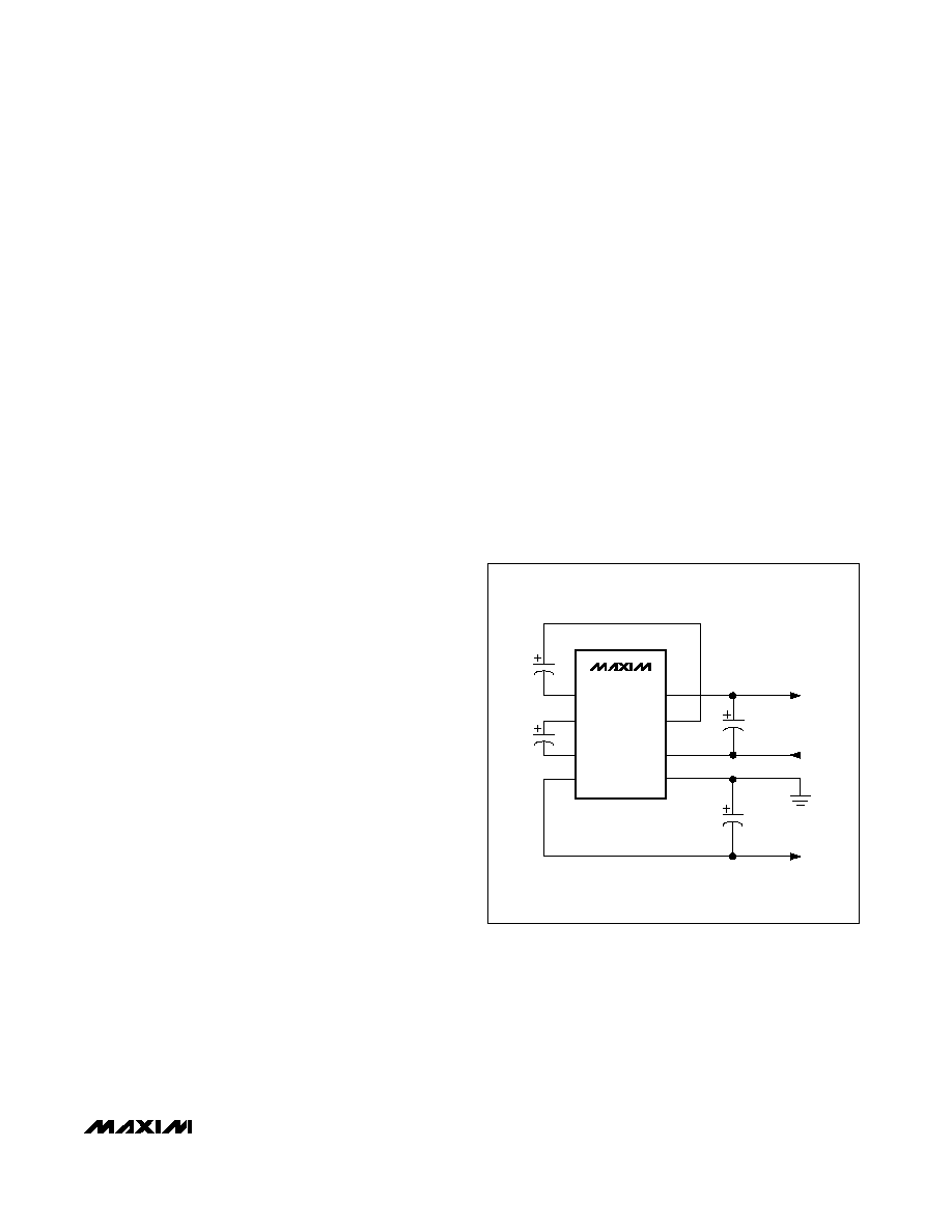
Positive and Negative Converter
The most common application of the MAX680/MAX681
is as a dual charge-pump voltage converter that pro-
vides positive and negative outputs of two times a posi-
tive input voltage. For applications where PC board
space is at a premium, the MAX681, with its capacitors
internal to the package, offers the smallest footprint.
The simple circuit shown in Figure 3 performs the same
function using the MAX680 with external capacitors C1
and C3 for the positive pump and C2 and C4 for the
negative pump. In most applications, all four capacitors
are low-cost, 10µF or 22µF polarized electrolytics.
When using the MAX680 for low-current applications,
1µF can be used for C1 and C2 charge-pump capaci-
tors, and 4.7µF for C3 and C4 reservoir capacitors.
C1 and C3 must be rated at 6V or greater, and C2 and
C4 must be rated at 12V or greater.
MAX680/MAX681
+5V to ±10V Voltage Converters
_______________________________________________________________________________________
5
MAX680
C1
22
µ
F
C3
22
µ
F
V+ OUT
V- OUT
V
CC
IN
GND
C4
22
µ
F
C2
22
µ
F
C1-
8
7
6
5
C2+
V-
V+
1
2
3
4
C1+
V
CC
GND
C2-
Figure 3. Positive and Negative Converter