General Description
The MAX6832≠MAX6840 are microprocessor (µP)
supervisory circuits used to monitor low-voltage power
supplies in µP and digital systems. They provide excel-
lent circuit reliability and low cost by eliminating exter-
nal components and adjustments when used with
+1.2V to +1.8V powered circuits.
These devices assert a reset signal whenever the V
CC
supply voltage declines below a preset threshold or
whenever manual reset (MR) is asserted. Reset remains
asserted for a fixed timeout delay after V
CC
has risen
above the reset threshold or when manual reset is
deasserted. Five different timeout periods are available:
70µs (voltage detector), 1.5ms, 30ms, 210ms, and 1.68s.
Reset thresholds suitable for operation with a variety of
supply voltages are available.
The MAX6832/MAX6835/MAX6838 have a push-pull
active-low reset output (RESET). The MAX6833/
MAX6836/MAX6839 have a push-pull active-high reset
output (RESET) and the MAX6834/MAX6837/MAX6840
have an open-drain active-low reset output (RESET). The
open-drain active-low reset output requires a pullup resis-
tor that can be connected to a voltage higher than V
CC
.
The MAX6835/MAX6836/MAX6837 feature a debounced
manual reset input (MR), while the MAX6838/MAX6839/
MAX6840 provide a RESET-IN input allowing the user to
externally adjust the reset threshold. The reset compara-
tor is designed to ignore fast transients on V
CC
.
Low supply current of 7.5µA makes the MAX6832≠
MAX6840 ideal for use in portable equipment. These
devices are available in 3- and 4-pin SC70 packages.
Applications
Computers
Controllers
Intelligent Instruments
Critical µP and µC Power Monitoring
Portable/Battery-Powered Equipment
Features
o Factory-Set Reset Threshold Voltages for
Nominal Supplies from 1.2V to 1.8V
o Low Power Consumption: 7.5µA (typ)
o Space-Saving 3- and 4-Pin SC70 Packages
o ±2.5% Reset Threshold Accuracy Over
Temperature
o Five Different Timeout Periods Available: 70µs
(voltage detector), 1.5ms, 30ms, 210ms, and 1.68s
o Three Reset Output Configurations
Push-Pull RESET
Push-Pull RESET
Open-Drain RESET
o Guaranteed Reset Valid to V
CC
=
0.55V--Active-Low
0.75V--Active-High
o Adjustable Threshold Reset-In Option
o Manual Reset Input Option
o Immune to Short Negative V
CC
Transients
o Pin Compatible with MAX803/MAX809/MAX810,
MAX6711/MAX6712/MAX6713, and
MAX6381≠MAX6390 Series
MAX6832≠MAX6840
Ultra-Low-Voltage SC70 Voltage Detectors
and µP Reset Circuits
________________________________________________________________ Maxim Integrated Products
1
Ordering Information
19-2242; Rev 1; 1/02
For pricing, delivery, and ordering information, please contact Maxim/Dallas Direct! at
1-888-629-4642, or visit Maxim's website at www.maxim-ic.com.
Pin Configurations appear at end of data sheet.
Typical Operating Circuit apears at end of data sheet.
Selector Guide appears at end of data sheet.
PART
TEMP. RANGE
PIN-PACKAGE
MAX6832_XRD_-T
-40
∞C to +85∞C
3 SC70-3
MAX6833_XRD_-T
-40
∞C to +85∞C
3 SC70-3
MAX6834_XRD_-T
-40
∞C to +85∞C
3 SC70-3
MAX6835_XSD_-T
-40
∞C to +85∞C
4 SC70-4
MAX6836_XSD_-T
-40
∞C to +85∞C
4 SC70-4
MAX6837_XSD_-T
-40
∞C to +85∞C
4 SC70-4
MAX6838XSD_-T
-40
∞C to +85∞C
4 SC70-4
MAX6839XSD_-T
-40
∞C to +85∞C
4 SC70-4
MAX6840XSD_-T
-40
∞C to +85∞C
4 SC70-4
Insert the desired suffix letter from the Threshold Suffix Guide
(MAX6832≠MAX6837) and the Active Timeout Period Guide
tables into the blanks to complete the part number. Sample
stock is generally available on standard versions only (see
Standard Versions table). Standard versions require a minimum
order increment of 2.5k units. Nonstandard versions must be
ordered in 10k unit increments. Contact factory for availability.
All parts are offered in tape-and-reel only.
MAX6832≠MAX6840
Ultra-Low-Voltage SC70 Voltage Detectors
and µP Reset Circuits
2
_______________________________________________________________________________________
ABSOLUTE MAXIMUM RATINGS
ELECTRICAL CHARACTERISTICS
(V
CC
= +0.55V to +3.6V, T
A
= T
MIN
to T
MAX
, unless otherwise noted. Typical values are at T
A
= +25∞C.) (Note 1)
Stresses beyond those listed under "Absolute Maximum Ratings" may cause permanent damage to the device. These are stress ratings only, and functional
operation of the device at these or any other conditions beyond those indicated in the operational sections of the specifications is not implied. Exposure to
absolute maximum rating conditions for extended periods may affect device reliability.
Terminal Voltage (with respect to GND)
V
CC
........................................................................-0.3V to +6.0V
Open-Drain RESET, MR .......................................-0.3V to +6.0V
RESET-IN, Push-Pull RESET
and RESET ..............................................-0.3V to (V
CC
+ 0.3V)
Input/Output Current (all pins) ............................................20mA
Continous Power Dissipation (T
A
= +70∞C)
3-Pin SC70 (derate 2.9mW/∞C above +70∞C) ...............235mW
4-Pin SC70 (derate 3.1mW/∞C above +70∞C) ...............245mW
Operating Temperature Range ...........................-40∞C to +85∞C
Junction Temperature ......................................................+150∞C
Storage Temperature Range .............................-65∞C to +150∞C
Lead Temperature (soldering, 10s) .................................+300∞C
PARAMETER
SYMBOL
CONDITIONS
MIN
TYP
MAX
UNITS
T
A
= -40
∞C to +85∞C
MAX6832/MAX6835/MAX6838
MAX6834/MAX6837/MAX6840
0.55
3.6
T
A
= -40
∞C to +85∞C
MAX6833/MAX6836/MAX6839
0.85
3.6
Supply Voltage Range
V
CC
T
A
= 0
∞C to +85∞C
MAX6833/MAX6836/MAX6839
0.75
3.6
V
V
CC
= 1.2V, no load, reset not asserted
7.5
13
V
CC
= 1.8V, no load, reset not asserted
9
16
Supply Current
I
CC
V
CC
= 3.6V, no load, reset not asserted
16
25
µA
W
1.620
1.665
1.710
V
1.530
1.575
1.620
I
1.350
1.388
1.425
H
1.275
1.313
1.350
G
1.080
1.110
1.140
Reset Threshold
V
TH
F (Note 2)
1.020
1.050
1.080
V
1.1V
V
CC
3.3V, 0∞C to +85∞C
-2.5%
444
+2.5%
RESET-IN Threshold
V
RSTIN
1.1V
V
CC
3.3V, -40∞C to +85∞C
-3.0%
444
+3.0%
mV
RESET-IN Leakage Current
I
RSTIN
-25
+25
nA
Reset Threshold Hysteresis
V
HYS
0.75
%V
TH
V
CC
or RESET-IN to Reset Delay
V
CC
falling, step signal from
(V
TH
+ 100mV) to (V
TH
- 100mV)
60
µs
D0
0.07
D1
1
1.5
2
D2
20
30
40
D3
140
210
280
Reset Active Timeout Period
t
RP
D4
1120
1680
2240
ms
MAX6832≠MAX6840
Ultra-Low-Voltage SC70 Voltage Detectors
and µP Reset Circuits
_______________________________________________________________________________________
3
ELECTRICAL CHARACTERISTICS (continued)
(V
CC
= +0.55V to +3.6V, T
A
= T
MIN
to T
MAX
, unless otherwise noted. Typical values are at T
A
= +25∞C.) (Note 1)
PARAMETER
SYMBOL
CONDITIONS
MIN
TYP
MAX
UNITS
Propagation Delay (D0 only)
t
P
V
CC
rising, step signal
from (V
TH
- 100mV) to (V
TH
+ 100mV)
70
µs
Startup Time (D0 only)
V
CC
rising from 0 to 1.1V (t
R
< 1µs)
150
µs
V
IL
0.3 x V
CC
MR Input Voltage
V
IH
0.7 x V
CC
V
MR Minimum Input Pulse Width
MR driven from V
CC
to 0
2
µs
MR Glitch Rejection
MR driven from V
CC
to 0
100
ns
MR to Reset Delay
MR driven from V
CC
to 0
500
ns
MR Pullup Resistance To V
CC
14
20
26
k
V
CC
0.55V, I
SINK
=15µA, reset asserted
0.15
V
CC
1.0V, I
SINK
= 80µA, reset asserted
0.15
Open-Drain RESET Output
Voltage
V
OL
V
CC
1.5V, I
SINK
= 200µA, reset asserted
0.2
V
Open-Drain RESET Output
Leakage Current
I
LKG
V
CC
> V
TH,
reset not asserted
1.0
µA
V
CC
0.55V, I
SINK
= 15µA, reset asserted
0.2 x V
CC
V
CC
1.0V, I
SINK
= 80µA, reset asserted
0.2 x V
CC
V
OL
V
CC
1.5V, I
SINK
= 200µA, reset asserted
0.2 x V
CC
V
CC
1.1V, I
SOURCE
= 50µA, reset not
asserted
0.8 x V
CC
Push-Pull RESET Output
Voltage
V
OH
V
CC
1.5V, I
SOURCE
= 150µA, reset asserted
0.8 x V
CC
V
CC
0.75V, I
SOURCE
= 10µA, reset asserted
(Note 2)
0.8 x V
CC
V
CC
0.85V, I
SOURCE
= 10µA, reset asserted
0.8 x V
CC
V
CC
1.0V, I
SOURCE
= 50µA, reset asserted
0.8 x V
CC
V
OH
V
CC
1.5V, I
SOURCE
= 150µA, reset asserted
0.8 x V
CC
V
CC
1.1V, I
SINK
= 80µA, reset not asserted
0.2 x V
CC
Push-Pull RESET Output
Voltage
V
OL
V
CC
1.5V, I
SINK
= 200µA, reset not asserted
0.2 x V
CC
V
Note 1: 100% production tested at +25∞C. Over temperature limits are guaranteed by design.
Note 2: Temperature range is from 0∞C to +85∞C.
MAX6832≠MAX6840
Ultra-Low-Voltage SC70 Voltage Detectors
and µP Reset Circuits
4
_______________________________________________________________________________________
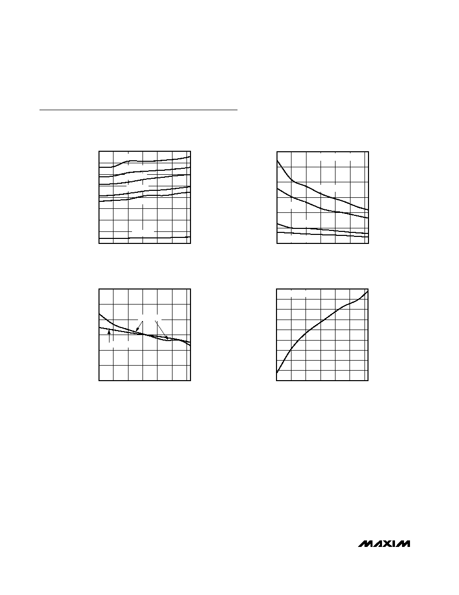
Typical Operating Characteristics
(V
CC
= full range and T
A
= -40∞C to +85∞C, unless otherwise noted. Typical values are at T
A
= +25∞C).
SUPPLY CURRENT vs. TEMPERATURE
MAX6832-40 toc01
0
2
6
4
12
14
10
8
16
SUPPLY CURRENT (
µ
A)
-40
0
20
-20
40
60
80
TEMPERATURE (
∞C)
V
CC
= 3.6V
V
CC
= 3.0V
V
CC
= 2.5V
V
CC
= 1.8V
V
CC
= 1.5V
V
CC
= 0.55V
0
100
50
200
150
250
300
-40
20
40
-20
0
60
80
POWER-DOWN RESET DELAY
vs. TEMPERATURE
MAX6832-40 toc02
TEMPERATURE (
∞C)
POWER-DOWN RESET DELAY (
µ
s)
V
OD
= OVERDRIVE (mV)
V
OD
= 10mV
V
OD
= 20mV
V
OD
= 100mV
V
OD
= 200mV
0.994
0.996
0.995
0.999
0.998
0.997
1.002
1.001
1.000
1.003
-40
0
-20
20
40
60
80
NORMALIZED RESET THRESHOLD
vs. TEMPERATURE
MAX6832-40 toc04
TEMPERATURE (
∞C)
NORMALIZED RESET THRESHOLD
V
TH
= 1.665V
0.94
0.98
0.96
1.02
1.00
1.04
1.06
-40
20
40
-20
0
60
80
NORMALIZED POWER-UP RESET
TIMEOUT vs. TEMPERATURE
MAX6832-40 toc03
TEMPERATURE (
∞C)
NORMALIZED RESET TIMEOUT PERIOD
D1 OPTION
D2 OPTION
MAX6832≠MAX6840
Ultra-Low-Voltage SC70 Voltage Detectors
and µP Reset Circuits
_______________________________________________________________________________________
5
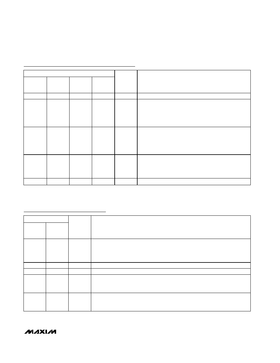
Pin Description--MAX6832≠MAX6837
PIN
MAX6833
SC70-3
MAX6832/
MAX6834
SC70-3
MAX6836
SC70-4
MAX6835/
MAX6837
SC70-4
NAME
FUNCTION
1
1
1
1
GND
Ground
--
2
--
2
RESET
Reset Output, Open-Drain or Push-Pull, Active-Low. RESET
changes from HIGH to LOW when V
CC
drops below the
selected reset threshold or MR is pulled low. RESET remains
LOW for the reset timeout period after V
CC
exceeds the device
reset threshold and MR is released high.
2
--
2
--
RESET
Reset Output, Push-Pull, Active-High. RESET changes from
LOW to HIGH when the V
CC
input drops below the selected
reset threshold or MR is pulled low. RESET remains HIGH for
the reset timeout period after V
CC
exceeds the device reset
threshold and MR is released high.
--
--
3
3
MR
Active-Low Manual Reset Input. Internal 20k
pullup to V
CC
.
Pull LOW to force a reset. Reset remains active as long as MR is
LOW and for the reset timeout period after MR goes HIGH.
Leave unconnected or connect to V
CC
if unused.
3
3
4
4
V
CC
Supply Voltage and Monitored Supply
Pin Description--MAX6838/MAX6839/MAX6840
PIN
MAX6839
SC70-4
MAX6838/
MAX6840
SC70-4
NAME
FUNCTION
1
1
RESET-IN
Adjustable Reset Threshold Input. High-impedance input for reset comparator. Connect
this pin to an external resistive-divider network to set the reset threshold voltage; the
typical threshold is 444mV. Reset is asserted when RESET-IN is below the threshold (V
CC
is not monitored).
2
2
V
CC
Supply Voltage (1.1V to 3.3V)
3
3
GND
Ground
4
--
RESET
Reset Output, Push-Pull, Active-High. RESET changes from LOW to HIGH when the
RESET-IN input drops below the typical reset threshold (444mV). RESET remains HIGH for
the reset timeout period after RESET-IN exceeds the reset threshold.
--
4
RESET
Reset Output, Open-Drain or Push-Pull, Active-Low. RESET changes from HIGH to LOW
when RESET-IN drops below the typical reset threshold (444mV). RESET remains LOW for
the reset timeout period after RESET-IN exceeds the reset threshold.