 | –≠–ª–µ–∫—Ç—Ä–æ–Ω–Ω—ã–π –∫–æ–º–ø–æ–Ω–µ–Ω—Ç: MAX686EEE | –°–∫–∞—á–∞—Ç—å:  PDF PDF  ZIP ZIP |
General Description
The MAX686 DAC-controlled boost/inverter IC converts
a positive input voltage to a positive or negative LCD
bias voltage up to +27.5V or -27.5V. The device features
an internal N-channel MOSFET switch, programmable
current limiting, and an internal 6-bit digital-to-
analog converter (DAC) for digital adjustment of the
output voltage. It comes in a small 16-pin QSOP pack-
age (same size as an 8-pin SO).
The MAX686 uses a current-limited, pulse-frequency-
modulation (PFM) control scheme to provide high effi-
ciency over a wide range of load conditions. Its high
switching frequency (up to 300kHz) allows the use of
small external components.
An LCDON output allows the LCD bias voltage to be
automatically disabled when the display logic voltage is
removed, protecting the display. The MAX686 has a
+2.7V to +5.5V input voltage range for the IC, and a
+0.8V to +27.5V input voltage range for the inductor.
Typical quiescent supply current is 65µA. Shutdown
current is 1.5µA.
The MAX686 offers high-level integration to save space,
reduce power consumption, and increase battery life,
making it an excellent choice for battery-powered
portable equipment. The MAX629 is similar to the
MAX686, except that it does not contain a built-in DAC.
Both devices have evaluation kits to facilitate designs.
Applications
Positive or Negative LCD Bias
Personal Digital Assistants
Notebook Computers
Portable Data-Collection Terminals
Palmtop Computers
Varactor Tuning Diode Bias
____________________________Features
o
Internal 500mA, 28V N-Channel Switch
(no external FET required)
o
Adjustable Output Voltage to +27.5V or -27.5V
o
6-Bit DAC-Controlled Output Voltage
o
Up to 90% Efficiency
o
Small 16-Pin QSOP Package
(Same size as 8-pin SO)
o
Power-OK Indicator
o
65µA Quiescent Current
o
1.5µA Shutdown Current
o
Up to 300kHz Switching Frequency
MAX686
DAC-Controlled Boost/Inverter
LCD Bias Supply with Internal Switch
________________________________________________________________
Maxim Integrated Products
1
19-1327; Rev 1; 2/98
PART
MAX686C/D
MAX686EEE
-40∞C to +85∞C
0∞C to +70∞C
TEMP. RANGE
PIN-PACKAGE
Dice*
16 QSOP
EVALUATION KIT
AVAILABLE
Ordering Information
*
Dice are specified at T
A
= +25∞C, DC parameters only.
For free samples & the latest literature: http://www.maxim-ic.com, or phone 1-800-998-8800.
For small orders, phone 408-737-7600 ext. 3468.
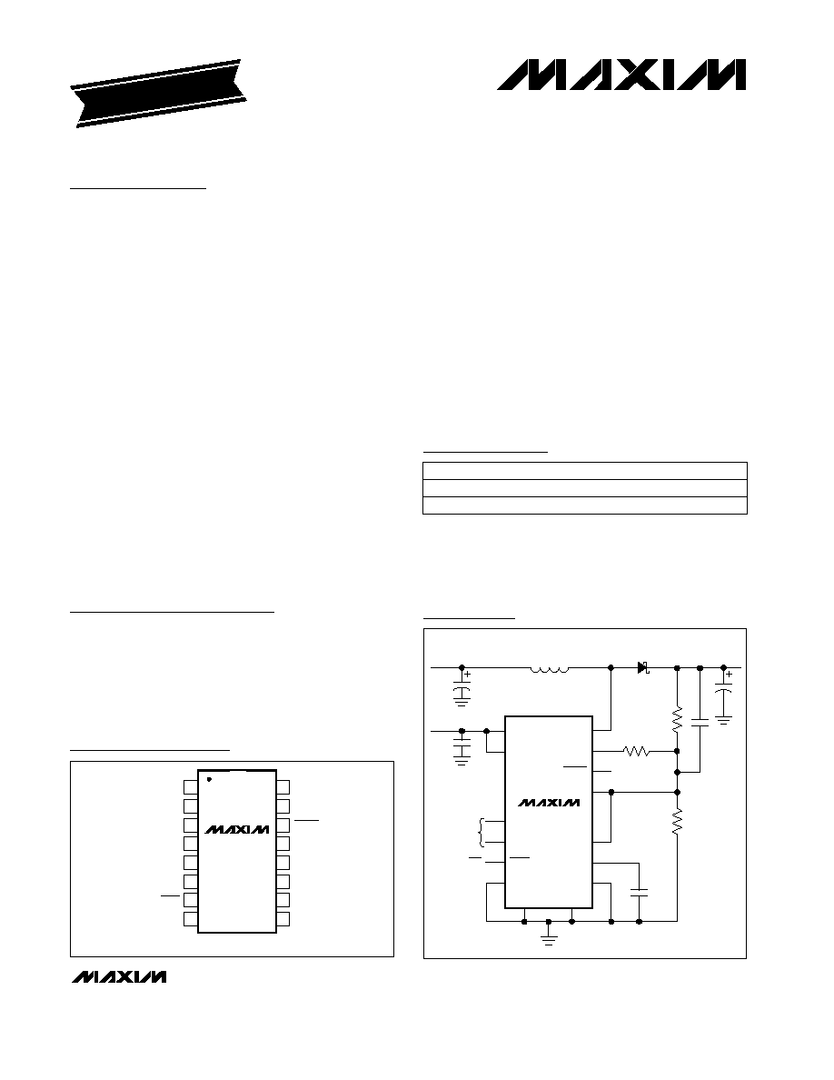
Functional Diagram appears at end of data sheet.
MAX686
V
CC
V
DD
V
OUT
22
µ
H
V
IN
= 0.8V TO 27.5V
UP
SHDN
DN
POL
GND
PGND
LX
DACOUT
LCDON
FB
REF
POK
ISET
0.1
µ
F
R3
R2
MBR0530L
R1
ON/OFF
DAC CONTROL
V
CC
= 2.7V TO 5.5V
0.1
µ
F
Typical Operating Circuit
16
15
14
13
12
11
10
9
1
2
3
4
5
6
7
8
PGND
LX
N.C.
LCDON
GND
POK
FB
REF
TOP VIEW
MAX686
QSOP
UP
DN
ISET
POL
V
DD
V
CC
SHDN
DACOUT
Pin Configuration
MAX686
DAC-Controlled Boost/Inverter
LCD Bias Supply with Internal Switch
2
_______________________________________________________________________________________
ABSOLUTE MAXIMUM RATINGS
ELECTRICAL CHARACTERISTICS
(V
CC
= V
DD
= V
IN
= +5V, C
REF
= 0.1µF,
T
A
= 0∞C to +85∞C,
unless otherwise noted. Typical values are at T
A
= +25∞C.)
Stresses beyond those listed under "Absolute Maximum Ratings" may cause permanent damage to the device. These are stress ratings only, and functional
operation of the device at these or any other conditions beyond those indicated in the operational sections of the specifications is not implied. Exposure to
absolute maximum rating conditions for extended periods may affect device reliability.
Voltage
V
CC
, ISET, POK, POL, SHDN,
UP, DN, V
DD
to GND ...........................................-0.3V to +6V
FB, REF, DACOUT to GND.......................-0.3V to (V
CC
+ 0.3V)
PGND to GND .....................................................-0.3V to +0.3V
LX, LCDON to GND..............................................-0.3V to +30V
Current
LX (sinking) .....................................................................600mA
LCDON (sinking)...............................................................10mA
Continuous Power Dissipation (T
A
= +70∞C)
QSOP (derate 8.30mW/∞C above +70∞C) ......................667mW
Operating Temperature Ranges
MAX686C/D ..........................................................0∞C to +70∞C
MAX686EEE.......................................................-40∞C to +85∞C
Storage Temperature Range .............................-65∞C to +160∞C
Lead Temperature (soldering, 10sec) .............................+300∞C
SHDN = GND
POL = GND, V
FB
= 1.3V, I
DACOUT
= 0mA
Boost configuration, V
OUT
= 27.5V,
I
LOAD
= 0mA to 5mA
Boost configuration, V
OUT
= 27.5V,
I
LOAD
= 5mA, V
CC
= V
DD
= 2.7V to 5.5V
Rising or falling
CONDITIONS
µA
1.3
4
I
SHDN
Shutdown Current
µA
65
125
I
CC
+ I
DD
V
2.7
5.5
V
CC
, V
DD
Supply Voltage (Note 1)
Supply Current
V
28
V
LX
LX Voltage Range
%/mA
0.01
Load Regulation
%/V
0.1
Line Regulation
V
2.10
2.5
2.65
V
LOCK
V
CC
Undervoltage Lockout
mV
100
V
CC
Undervoltage Lockout
Hysteresis
V
0.5
1.5
2.1
V
RESET
V
CC
DAC Reset Threshold
UNITS
MIN
TYP
MAX
SYMBOL
PARAMETER
ISET = V
CC
A
0.42
0.50
0.58
I
LX
LX Switch Current Limit
ISET = GND
0.21
0.25
0.29
V
LX
= 28V
µA
1.5
I
LXLEAK
LX Leakage Current
V
CC
= V
DD
= 5V, I
LX
= 100mA
0.6
1.2
R
LX
LX On-Resistance
V
CC
= V
DD
= 3.3V, I
LX
= 100mA
0.8
1.6
µs
8
10
12
t
ON
Maximum LX On-Time
POL = GND, V
FB
> 1.2V
µs
0.8
1
1.2
t
OFF
Minimum LX Off-Time
POL = V
CC
, V
FB
< 0.15V
2.8
3.5
4.2
POL = GND, V
FB
< 0.8V
4
5
6
POL = V
CC
, V
FB
> 0.4V
4
5
6
Voltage applied to L1
V
0.8
V
OUT
V
IN
Input Voltage
LX
MAX686
DAC-Controlled Boost/Inverter
LCD Bias Supply with Internal Switch
_______________________________________________________________________________________
3
I
REF
= 0µA to 25µA, C
REF
= 0.1µF
V
CC
= V
DD
= 2.7V to 5.5V, no load
0µA < I
DACOUT
< 20µA
-50µA < I
DACOUT
< 0µA
I
REF
= 0µA to 50µA, C
REF
= 0.47µF
CONDITIONS
mV
1
10
REF Load Regulation
V
1.225
1.250
1.275
V
REF
REF Output Voltage
mV
0
15
V
ZS
Zero-Scale Output Voltage
V
V
REF
-
V
REF
V
REF
+
0.015
0.015
V
FS
Full-Scale Output Voltage
1.5
nA
±50
I
FB
FB Input Bias Current
UNITS
MIN
TYP
MAX
SYMBOL
PARAMETER
ELECTRICAL CHARACTERISTICS (continued)
(V
CC
= V
DD
= V
IN
= +5V, C
REF
= 0.1µF,
T
A
= 0∞C to +85∞C
, unless otherwise noted. Typical values are at T
A
= +25∞C.)
POL = GND
POL = V
CC
V
1.225
1.250
1.275
V
FB
FB Set Point
mV
-15
0
15
nA
±50
I
POK
POK Input Current
V
POK
rising
V
1.100
1.125
1.150
V
POK
POK Threshold
mV
12
POK Hysteresis
V
LCDON
= 0.4V, V
POK
= 1.25V
mA
2
6
I
LCDON
LCDON Sink Current
V
LCDON
= 28V, V
POK
= GND
µA
0.02
1
LCDON Leakage Current
bits
6
Resolution
Mid-scale = V
REF
x 32/63
%
-2
2
MSA
Mid-Scale Accuracy
Guaranteed monotonic
LSB
-1
1
DNL
Differential Nonlinearity
k
1.5
R
DACOUT
Output Resistance in Shutdown
2.7V < V
CC
= V
DD
< 5.5V
V
0.7
V
IL
Input Low Level
2.7V < V
CC
= V
DD
< 5.5V
V
2.4
V
IH
Input High Level
µA
±1
I
BIAS
Input Bias Current
UP, DN, T
A
= +25∞C
µs
1
t
PWH
Pulse Width High
UP, DN, T
A
= +25∞C
µs
1
t
PWL
Pulse Width Low
UP, DN, T
A
= +25∞C
µs
1
t
PWS
Pulse Separation
REFERENCE AND FB INPUT
POWER OK COMPARATOR,
LCDON
OUTPUT
DAC OUTPUT
(Notes 2, 3)
LOGIC INPUTS: POL, ISET, UP, DN,
SHDN
MAX686
DAC-Controlled Boost/Inverter
LCD Bias Supply with Internal Switch
4
_______________________________________________________________________________________
ISET = V
CC
A
0.4
0.6
SHDN = GND
I
LX
LX Switch Current Limit
POL = GND, VFB = 1.3V, I
DACOUT
= 0mA
ISET = GND
V
CC
= V
DD
= 5V, I
LX
= 100mA
0.2
0.3
1.2
V
LX
= 28V
Rising or falling
µA
1.5
CONDITIONS
I
LXLEAK
LX Leakage Current
R
LX
LX On-Resistance
V
CC
= V
DD
= 3.3V, I
LX
= 100mA
1.6
µs
7.5
12.5
t
ON
Maximum LX On-Time
POL = GND, V
FB
> 1.2V
µs
0.7
1.3
t
OFF
Minimum LX Off-Time
POL = V
CC
, V
FB
< 0.15V
2.8
4.2
POL = GND, V
FB
< 0.8V
3.8
6.2
POL = V
CC
, V
FB
> 0.4V
3.8
6.2
µA
4
I
SHDN
Shutdown Current
µA
125
I
CC
+ I
DD
V
2.7
5.5
V
CC
, V
DD
Supply Voltage (Note 1)
Supply Current
V
28
V
LX
LX Voltage Range
V
2.10
2.65
V
LOCK
V
CC
Undervoltage Lockout
UNITS
MIN
TYP
MAX
SYMBOL
PARAMETER
ELECTRICAL CHARACTERISTICS
(V
CC
= V
DD
= V
IN
= +5V, C
REF
= 0.1µF,
T
A
= -40∞C to +85∞C
, unless otherwise noted.) (Note 4)
Note 1:
The MAX686 requires a supply voltage at V
CC
= V
DD
between +2.7V and +5.5V; however, the voltage that supplies the
inductor can vary from +0.8V to +27.5V, depending on circuit operating conditions.
Note 2:
The DAC output is set to its midpoint value at power-on.
Note 3:
The DAC setting is guaranteed to remain valid as long as V
CC
is greater than the V
CC
DAC Reset Threshold.
Note 4:
Specifications to -40∞C are guaranteed by design, not production tested.
V
CC
= V
DD
= 2.7V to 5.5V, no load
V
1.22
1.28
V
REF
REF Output Voltage
I
REF
= 0µA to 25µA, C
REF
= 0.1µF
mV
10
REF Load Regulation
POL = GND
V
1.22
1.28
V
FB
FB Set Point
POL = V
CC
-15
15
nA
±50
I
FB
FB Input Bias Current
V
POK
rising
V
1.05
1.20
V
POK
POK Threshold
nA
±50
I
POK
POK Input Current
V
LCDON
= 0.4V, V
POK
= 1.25V
mA
2
I
LCDON
LCDON Sink Current
mV
Voltage applied to L1
V
0.8
V
OUT
V
IN
Input Voltage
-50µA < I
DACOUT
< 0µA
V
V
REF
-
V
REF
+
0.02
0.02
V
FS
Full-Scale Output Voltage
0µA < I
DACOUT
< 20µA
mV
0
15
V
ZS
Zero-Scale Output Voltage
Bits
6
Resolution
Mid-scale = V
REF
x 32/63
%
-3
3
MSA
Mid-Scale Accuracy
2.7V < V
CC
= V
DD
< 5.5V
V
0.7
V
IL
Input Low Level
2.7V < V
CC
= V
DD
< 5.5V
V
2.4
V
IH
Input High Level
µA
±1
I
BIAS
Input Bias Current
LX
REFERENCE AND FB INPUT
POWER OK COMPARATOR,
LCDON
OUTPUT
LOGIC INPUTS: POL, ISET, UP, DN,
SHDN
DAC OUTPUT
(Notes 2, 3)
MAX686
DAC-Controlled Boost/Inverter
LCD Bias Supply with Internal Switch
_______________________________________________________________________________________
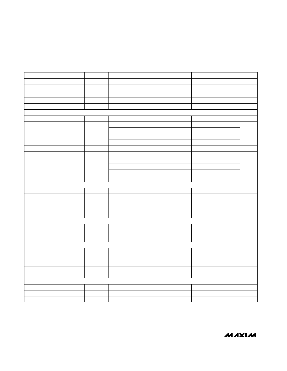
5
95
60
0.1
1
10
100
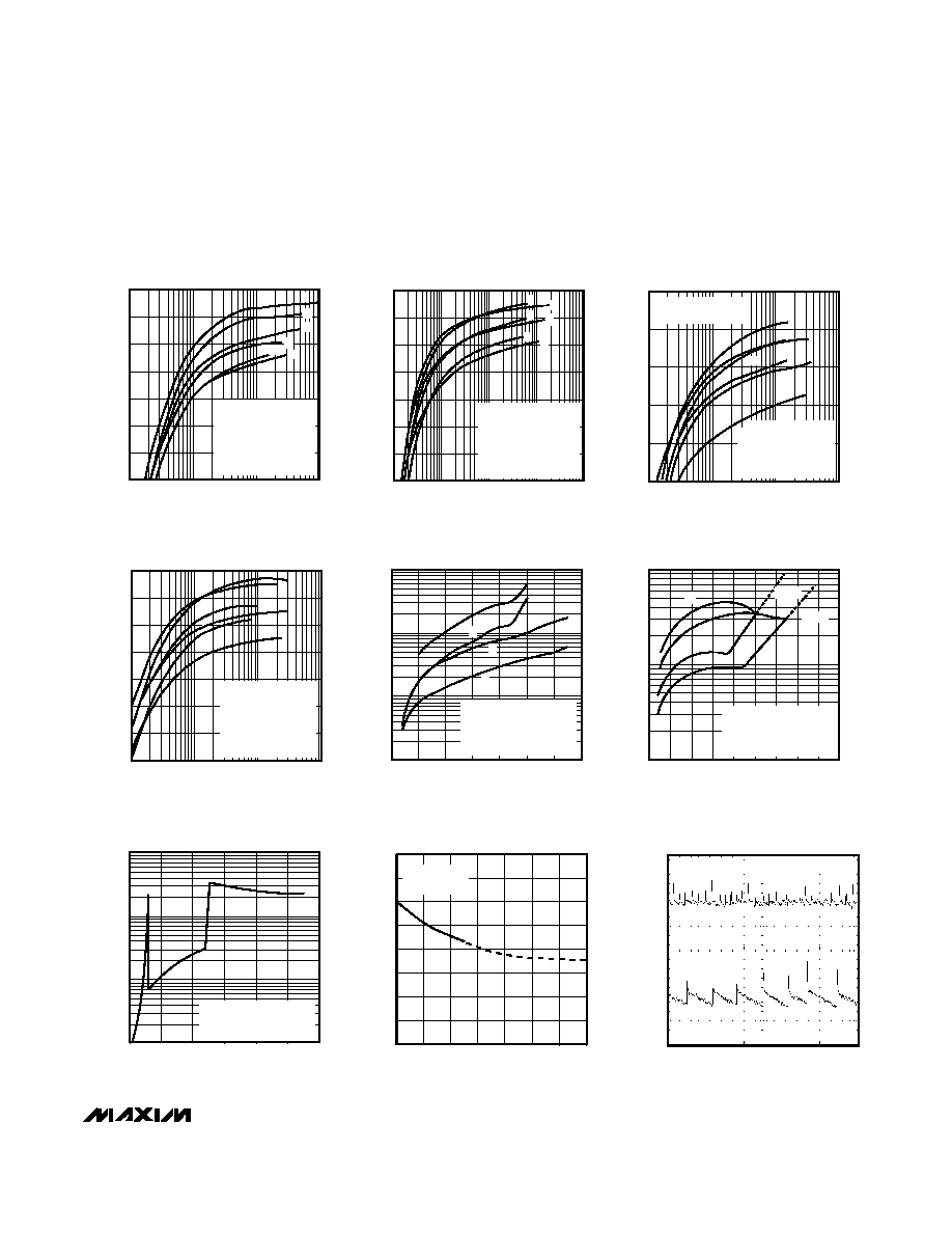
EFFICIENCY vs. LOAD CURRENT
(V
OUT
= +24V)
70
65
75
80
85
90
MAX686 TOC01
LOAD CURRENT (mA)
EFFICIENCY (%)
A: V
IN
= 12V, ISET = V
CC
B: V
IN
= 12V, ISET = GND
C: V
IN
= 5V, ISET = V
CC
D: V
IN
= 5V, ISET = GND
E: V
IN
= 3V, ISET = GND
F: V
IN
= 3V, ISET = V
CC
C
D
E
F
A
B
95
90
60
0.1
10
1
1000
100
EFFICIENCY vs. LOAD CURRENT
(V
OUT
= +12V)
65
MAX686 TOC02
LOAD CURRENT (mA)
EFFICIENCY (%)
70
75
80
85
A: V
IN
= 9V, ISET = V
CC
B: V
IN
= 9V, ISET = GND
C: V
IN
= 5V, ISET = V
CC
D: V
IN
= 5V, ISET = GND
E: V
IN
= 3V, ISET = GND
F: V
IN
= 3V, ISET = V
CC
D
C
F
B
A
E
85
60
0.1
1
10
100
EFFICIENCY vs. LOAD CURRENT
(V
OUT
= -12V)
65
70
75
80
MAX686 TOC03
LOAD CURRENT (mA)
EFFICIENCY (%)
A
F
E
B
D
C: V
IN
= 5V, ISET = GND
D: V
IN =
5V, ISET = V
CC
E: V
IN =
3V, ISET = GND
F: V
IN
= 3V, ISET = V
CC
A: V
IN
= 9V, ISET = GND
B: V
IN
= 9V, ISET = V
CC
C
__________________________________________Typical Operating Characteristics
(Circuits of Figures 1 and 2, V
CC
= V
DD
= V
IN
= +5V, L1 = 22µH, SHDN = V
CC
, C
REF
= 0.1µF, TA = +25∞C, unless otherwise noted.)
85
50
0.1
1
10
100
EFFICIENCY vs. LOAD CURRENT
(V
OUT
= -18V)
60
55
65
70
75
80
MAX686 TOC04
LOAD CURRENT (mA)
EFFICIENCY (%)
C
D
A: V
IN
= 9V, ISET = GND
B: V
IN
= 9V, ISET = V
CC
C: V
IN
= 5V, ISET = GND
D: V
IN
= 5V, ISET = V
CC
E: V
IN
= 3V, ISET = GND
F: V
IN
= 3V, ISET = V
CC
E
F
A
B
1000
1
0
4
6
2
10
12
8
14
MAXIMUM OUTPUT CURRENT vs.
INPUT VOLTAGE (V
OUT
= +12V, +24V)
10
100
MAX686 TOC05
INPUT VOLTAGE (V)
OUTPUT CURRENT (mA)
A: V
OUT
= 12V, ISET = V
CC
B: V
OUT
= 12V, ISET = GND
C: V
OUT
= 24V, ISET = V
CC
D: V
OUT
= 24V, ISET = GND
A
C
D
B
1
10
100
0
4
6
8
2
10
12
14
16
18
MAXIMUM OUTPUT CURRENT vs.
INPUT VOLTAGE (V
OUT
= -12V, -18V)
MAX686 TOC06
INPUT VOLTAGE (V)
OUTPUT CURRENT (mA)
B
D
C
A: V
OUT
= -12V, ISET = V
CC
B: V
OUT
= -18V, ISET = V
CC
C: V
OUT
= -12V, ISET = GND
D: V
OUT
= -18V, ISET = GND
A
B & D
A & C
V
OUT
50mV/div
AC-COUPLED
V
OUT
50mV/div
AC-COUPLED
ISET = V
CC
ISET
= GND
OUTPUT VOLTAGE RIPPLE
MAX686 TOC09
20
µ
s/div
V
OUT
= 24V
I
LOAD
= 5mA
1000
1
0
2
1
4
5
3
6
INPUT CURRENT
vs. INPUT VOLTAGE
10
100
MAX686 TOC07
INPUT VOLTAGE (V)
INPUT CURRENT (
µ
A)
V
CC
= V
IN
= V
DD
INPUT CURRENT = I
CC
+ I
DD
V
OUT
= 18V, NO LOAD
1.244
1.246
1.245
1.248
1.247
1.251
1.250
1.249
1.252
0
40
20
60
80
100
120
140
REFERENCE VOLTAGE
vs. LOAD CURRENT
MAX686
TOC08
LOAD CURRENT (
µ
A)
REFERENCE VOLTAGE (V)
V
IN
= V
CC
= 5V
C
REF
= 0.1
µ
F