General Description
The MAX6880≠MAX6883 dual-/triple-voltage monitors
are designed to sequence power supplies during
power-up condition. When all of the voltages exceed
their respective thresholds, these devices turn on volt-
ages to the system sequentially, enhancing n-channel
MOSFETs used as switches. The time between each
sequenced voltage is determined by an external
capacitor, thus allowing flexibility in delay timing. The
MAX6880/MAX6881 sequence three voltages and the
MAX6882/MAX6883 sequence two voltages.
These devices initially monitor all of the voltages and
when all of them are within their tolerances, the inter-
nal charge pumps enhance external n-channel
MOSFETs in a sequential manner to apply the volt-
ages to the system. Internal charge pumps drive the
gate voltages 5V above the respective input voltage
thereby ensuring the MOSFETs are fully enhanced to
reduce the on-resistance.
The MAX6880≠MAX6883 feature capacitor-adjustable
slew-rate control to provide controlled turn-on charac-
teristics. After all of the voltages reach 92.5% of their
final value, a power-good output (MAX6880/MAX6882)
signal is active. The power-good output (PG/RST) can
be delayed with an external capacitor to create a
power-on reset delay. After the initial power-up phase,
the MAX6880≠MAX6883 continue to monitor the volt-
ages. If any of the voltages falls below its threshold, the
MOSFETs are quickly turned off and the voltages are
tracked down together. An internal 100 pulldown
resistor ensures that the capacitance at the MOSFET's
source is discharged quickly. The power-good output
goes low to provide a system reset.
The MAX6880≠MAX6883 are available in small 4mm x
4mm 24-pin and 16-pin thin QFN packages and speci-
fied over the -40∞C to +85∞C extended operating tem-
perature range.
Applications
Multivoltage Systems
Networking Systems
Telecom
Storage Equipment
Servers/Workstations
Features
Capacitor-Adjustable Power-Up Sequencing
Delay
Internal Charge Pumps to Enhance External
n-Channel FETs
Capacitor-Adjustable Timeout Period Power-Good
Output (MAX6880/MAX6882)
Adjustable Undervoltage Lockout or
Logic-Enable Input
Internal 100 Pulldown for Each Output to
Discharge Capacitive Load Quickly
0.5V to 5.5V Nominal IN_/OUT_ Range
2.7V to 5.5V Operating Voltage Range
Immune to Short Voltage Transients
Small 4mm x 4mm 24-Pin or 16-Pin Thin QFN
Packages
MAX6880≠MAX6883
Dual-/Triple-Voltage, Power-Supply
Sequencers/Supervisors
________________________________________________________________ Maxim Integrated Products
1
23
24
22
21
8
7
9
ABP
SET2
SET1
EN/UV
10
N.C.
GATE3
N.C.
PG/RST
OUT2
MARGIN
1
2
IN3
4
5
6
17
18
16
14
13
IN2
IN1
TIMEOUT
*EXPOSED PADDLE CONNECTED TO GND.
SLEW
DELAY
GND
EP*
+
MAX6880
SET3
OUT3
3
15
GATE1
20
11
N.C.
OUT1
19
12
N.C.
GATE2
4mm x 4mm THIN QFN
TOP VIEW
Pin Configurations
Ordering Information
19-3772; Rev 0; 7/05
For pricing, delivery, and ordering information, please contact Maxim/Dallas Direct! at
1-888-629-4642, or visit Maxim's website at www.maxim-ic.com.
Ordering Information continued at end of data sheet.
+Denotes lead-free package.
*Future product--contact factory for availability.
Selector Guide appears at end of data sheet.
PART
TEMP RANGE
PIN-
PACKAGE
PKG
CODE
MAX6880ETG+
-40∞C to +85∞C
24 Thin QFN
T2444-4
MAX6880ETG
-40∞C to +85∞C
24 Thin QFN
T2444-4
MAX6881ETE+*
-40∞C to +85∞C
16 Thin QFN
T1644-4
MAX6881ETE*
-40∞C to +85∞C
16 Thin QFN
T1644-4
Pin Configurations continued at end of data sheet.
MAX6880≠MAX6883
Dual-/Triple-Voltage, Power-Supply
Sequencers/Supervisors
2
_______________________________________________________________________________________
ABSOLUTE MAXIMUM RATINGS
ELECTRICAL CHARACTERISTICS
(IN1, IN2, or IN3 = +2.7V to +5.5V, EN/UV = MARGIN = ABP, T
A
= -40∞C to +85∞C, unless otherwise specified. Typical values are
at T
A
= +25∞C, unless otherwise noted.) (Note 1)
Stresses beyond those listed under "Absolute Maximum Ratings" may cause permanent damage to the device. These are stress ratings only, and functional
operation of the device at these or any other conditions beyond those indicated in the operational sections of the specifications is not implied. Exposure to
absolute maximum rating conditions for extended periods may affect device reliability.
IN1, IN2, IN3.............................................................-0.3V to +6V
ABP .........................................-0.3V to the highest of V
IN1 -
V
IN3
SET1, SET2, SET3 ....................................................-0.3V to +6V
GATE1, GATE2, GATE3 .........................................-0.3V to +12V
OUT1, OUT2, OUT3 .................................................-0.3V to +6V
MARGIN ...................................................................-0.3V to +6V
PG/RST, EN/UV ........................................................-0.3V to +6V
DELAY, SLEW, TIMEOUT .........................................-0.3V to +6V
OUT_ Current....................................................................±50mA
GND Current.....................................................................±50mA
Input/Output Current (all pins except
OUT_ and GND) ...........................................................±20mA
Continuous Power Dissipation (T
A
= +70∞C)
16-Pin 4mm x 4mm Thin QFN
(derate 16.9mW/∞C above +70∞C) .............................1349mW
24-Pin 4mm x 4mm Thin QFN
(derate 20.8mW/∞C above +70∞C) .............................1667mW
Operating Temperature Range ...........................-40∞C to +85∞C
Storage Temperature Range .............................-65∞C to +150∞C
Maximum Junction Temperature .....................................+150∞C
Lead Temperature (soldering, 10s) .................................+300∞C
PARAMETER
SYMBOL
CONDITIONS
MIN
TYP
MAX
UNITS
Voltage on the highest of IN_ to ensure that
PG/RST is valid and GATE_ = 0
1.4
Operating Voltage Range
IN_
Voltage on the highest of IN_ to ensure the
device is fully operational
2.7
5.5
V
Supply Current
I
CC
IN1 = 5.5V, IN2 = IN3 = 3.3V, no load
1.1
1.8
mA
SET_ falling, T
A
= +25
o
C
0.4925
0.5
0.5075
SET_ Threshold Range
V
TH
SET_ falling, T
A
= -40
∞C to +85∞C
0.4875
0.5
0.5125
V
SET_ Threshold Hysteresis
V
TH_HYST
SET_ rising
0.5
%
SET_ Input Current
I
SET
SET_ = 0.5V
-100
+100
nA
V
EN_R
Input rising
1.286
EN/UV Input Voltage
V
EN_F
Input falling
1.22
1.25
1.28
V
EN/UV Input Current
I
EN
-5
+5
µA
EN/UV Input Pulse Width
t
EN
EN/UV falling, 100mV overdrive
7
µs
DELAY, TIMEOUT Output Current
I
D
(Notes 2, 3)
2.12
2.5
2.88
µA
DELAY, TIMEOUT Threshold
Voltage
V
CC
= 3.3V
1.25
V
SLEW Output Current
I
S
( N ote 4)
22.5
25
27.5
µA
Sequence Slew-Rate Timebase
Accuracy
SR
C
SLEW
= 200pF
-15
+15
%
Timebase/C
SLEW
Ratio
100pF < C
SLEW
< 1nF
104
k
S l ew - Rate Accur acy d ur i ng P ow er -
U p and P ow er - D ow n
C
SLEW
= 200pF, V
IN_
= 5.5V ( N ote 4)
-50
+50
%
(All voltages referenced to GND, unless otherwise noted.)
MAX6880≠MAX6883
Dual-/Triple-Voltage, Power-Supply
Sequencers/Supervisors
_______________________________________________________________________________________
3
Note 1: Specifications guaranteed for the stated global conditions. 100% production tested at T
A
= +25∞C and T
A
= +85∞C.
Specifications at T
A
= -40∞C to +85∞C are guaranteed by design. These devices meet the parameters specified when at
least one of IN1/IN2/IN3 is between 2.7V to 5.5V, while the remaining IN1/IN2/IN3 are between 0 and 5.5V.
Note 2: A current I
D
= 2.5µA ±15% is generated internally and is used to set the DELAY and TIMEOUT periods and used as a refer-
ence for t
DELAY
and t
TIMEOUT
.
Note 3: The total DELAY is t
DELAY
= 200µs + (500k x C
DELAY
). Leave DELAY unconnected for 200µs delay. The total TIMEOUT is
t
TIMEOUT
= 200µs + (500k x C
TIMEOUT
). Leave TIMEOUT unconnected for 200µs timeout.
Note 4: A current I
S
= 25µA ±10% is generated internally and used as a reference for t
FAULT
, t
RETRY
, and slew rate.
Note 5: During power-up, only the condition OUT_ < ramp - V
TRK
is checked in order to stop the ramp. However, both conditions
OUT_ < ramp ≠ V
TRK_F
and OUT_ > ramp + V
TRK_F
cause a fault. During power-down, only the condition OUT > ramp +
V
TRK
is checked in order to stop the ramp. However, both conditions OUT_ < ramp - V
TRK_F
and OUT_ > ramp + V
TRK_F
cause a fault (see Figure 10). Therefore, if OUT1, OUT2, and OUT3 (during power-up tracking and power-down) differ by
more than 2 x V
TRK_F
, a fault condition is asserted.
Note 6: A 100 pulldown to GND activated by a fault condition. See the Internal Pulldown section.
ELECTRICAL CHARACTERISTICS (continued)
(IN1, IN2, or IN3 = +2.7V to +5.5V, EN/UV = MARGIN = ABP, T
A
= -40∞C to +85∞C, unless otherwise specified. Typical values are
at T
A
= +25∞C, unless otherwise noted.) (Note 1)
Power-Good Threshold
V
TH_PG
V
OUT_
falling
91.5
92.5
93.5
%
Power-Good Threshold Hysteresis
V
HYS_PG
V
OUT_
rising
0.5
%
GATE_ Output High
V
GOH
I
SOURCE
= 0.5µA
IN_ +
4.2
IN_ +
5.0
IN_ +
5.8
V
GATE_ Pullup Current
I
GUP
During power-up and power-down,
V
GATE_
= 1V
2.5
4
µA
I
GD
During power-up and power-down,
V
GATE_
= 5V
2.5
4
µA
When disabled, V
GATE_
= 5V, V
IN_
2.7V
9.5
GATE_ Pulldown Current
I
GDS
When disabled, V
GATE_
= 5V, V
IN_
4V
20
mA
SET_ to GATE_ Delay
t
D-GATE
SET falling, 25mV overdrive
10
µs
V
IN_
2.7V, I
SINK
= 1mA, output asserted
0.3
PG/RST Output Low
V
OL
V
IN_
4.0V, I
SINK
= 4mA, output asserted
0.4
V
Tracking Differential Voltage Stop
Ramp
V
TRK
Differential between each of the OUT_ and
the ramp voltage during power-up and
power-down, Figure 1 (Note 5)
75
125
180
mV
Tracking Differential Fault Voltage
V
TRK_F
Differential between each of the OUT_ and
the ramp voltage, Figure 1 (Note 5)
200
250
310
mV
Power-Low Threshold
V
TH_PL
OUT_ falling
125
142
170
mV
Power-Low Hysteresis
V
TH_PLHYS
OUT_ rising
10
mV
OUT to GND Pulldown Impedance
IN_ > 2.7V (Note 6)
100
MARGIN Pullup Current
I
IN
7
10
13
µA
V
IL
0.8
MARGIN Input Voltage
V
IH
2.0
V
MARGIN Glitch Rejection
100
ns
MAX6880≠MAX6883
Dual-/Triple-Voltage, Power-Supply
Sequencers/Supervisors
4
_______________________________________________________________________________________
250mV DOWN =
FAULT THRESHOLD
250mV DOWN =
FAULT THRESHOLD
125mV DOWN =
STOP RAMP THRESHOLD
125mV UP =
STOP RAMP THRESHOLD
250mV UP =
FAULT THRESHOLD
250mV UP =
FAULT THRESHOLD
REFERENCE RAMP
REFERENCE RAMP
POWER-UP
POWER-DOWN
Figure 1. Stop Ramp/Fault Window During Power-Up and Power-Down
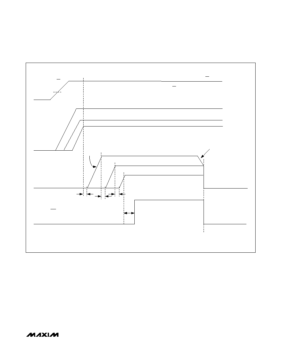
EN/UV
BUS VOLTAGE MONITORED THROUGH EN/UV INPUT
IN_
IN1 = 3.3V
IN2 = 1.8V
IN3 = 0.7V
OUT_
OUT1 = 3.3V
OUT2 = 1.8V
OUT3 = 0.7V
CAPACITOR-
ADJUSTED
SLEW RATE
PG/RST
MONITORED THROUGH SET THRESHOLDS ON SET_ INPUTS
t
DELAY
t
DELAY
t
DELAY
t
TIMEOUT
V
EN_R
EN/UV
V
EN_F
Figure 2. Sequencing In Normal Mode
MAX6880≠MAX6883
Dual-/Triple-Voltage, Power-Supply
Sequencers/Supervisors
_______________________________________________________________________________________
5
IN_
V
EN_R
IN1 = 3.3V
IN2 = 1.8V
IN3 = 0.7V
MONITORED THROUGH SET THRESHOLDS ON SET_ INPUTS
OUT_
OUT2 = 1.8V
OUT3 = 0.7V
OUT1 = 3.3V
EN/UV
EN/UV
BUS VOLTAGE MONITORED THROUGH EN/UV INPUT
FORCED INTO QUICK SHUTDOWN WHEN OUT1 FALLS BELOW 92.5% of IN1
OUT_ FORCED
BELOW V
TH_PG
CAPACITOR-
ADJUSTED
SLEW RATE
PG/RST
t
DELAY
t
DELAY
t
DELAY
t
TIMEOUT
Figure 3. Sequencing In Fast Shutdown Mode