 | –≠–ª–µ–∫—Ç—Ä–æ–Ω–Ω—ã–π –∫–æ–º–ø–æ–Ω–µ–Ω—Ç: MAX6952 | –°–∫–∞—á–∞—Ç—å:  PDF PDF  ZIP ZIP |

MAX6952
4-Wire Interfaced, 2.7V to 5.5V,
4-Digit 5
7 Matrix LED Display Driver
________________________________________________________________ Maxim Integrated Products
1
For pricing, delivery, and ordering information, please contact Maxim/Dallas Direct! at
1-888-629-4642, or visit Maxim's website at www.maxim-ic.com.
General Description
The MAX6952 is a compact cathode-row display driver
that interfaces microprocessors to 5
7 dot-matrix LED
displays through an SPITM-compatible serial interface.
The MAX6952 drives up to four digits (140 LEDs).
Included on chip are an ASCII 104-character font, mul-
tiplex scan circuitry, column and row drivers, and static
RAM that stores each digit, as well as font data for 24
user-definable characters. The segment current for the
LEDs is set by an internal digit-by-digit digital bright-
ness control.
The device includes a low-power shutdown mode, seg-
ment blinking (synchronized across multiple drivers, if
desired), and a test mode that forces all LEDs on. The
LED drivers are slew rate limited to reduce EMI.
For a 2-wire interfaced version, refer to the MAX6953
data sheet. An EV kit is available for the MAX6952.
Features
o High-Speed 26MHz with SPI-/QSPI-TM/
MICROWIRETM-Compatible Serial Interface
o 2.7V to 5.5V Operation
o Drives Four Monocolor or Two Bicolor Cathode-
Row 5
7 Matrix Displays
o Built-In ASCII 104-Character Font
o 24 User-Definable Characters Available
o Automatic Blinking Control for Each Segment
o 36µA Low-Power Shutdown (Data Retained)
o 16-Step Digital Brightness Control
o Display Blanked on Power-Up
o Slew-Rate-Limited Segment Drivers for Lower EMI
o 36-Pin SSOP and 40-Pin DIP Packages
Ordering Information
DIGIT 1
R1
R6
R7
C1
R4
R3
R2
R5
C2
C3
C5
C4
DIGIT 0
O0
O1
O2
O3
O4
O5
O6
O14
O15
O16
O17
O18
R1
R6
R7
C1
R4
R3
R2
R5
C2
C3
C5
C4
O0
O1
O2
O3
O4
O5
O6
O19
O20
O21
O22
O23
R1
R6
R7
C1
R4
R3
R2
R5
C2
C3
C5
C4
O7
O8
O9
O10
O11
O12
O13
O14
O15
O16
O17
O18
R1
R6
R7
C1
R4
R3
R2
R5
C2
C3
C5
C4
DIGIT 3
O7
O8
O9
O10
O11
O12
O13
O19
O20
O21
O22
O23
DIGIT 2
3.3V
100nF
47
µF
O0
O1
O2
O3
O4
O5
O6
O7
O8
O9
O10
O11
O12
O13
O14
O15
O16
O17
O18
O19
O20
O21
O22
O23
ISET
OSC
V+
V+
GND
GND
CS
GND
DIN
CLK
DOUT
C
SET
26pF
R
SET
53.6k
MAX6952
BLINK
3.3V
4.7k
Typical Application Circuit
19-2437; Rev 1; 10/02
EVALUATION KIT
AVAILABLE
PART
TEMP RANGE
PIN-PACKAGE
MAX6952EAX
-40∞C to +85∞C
36 SSOP
MAX6952EPL
-40∞C to +85∞C
40 PDIP
SPI and QSPI are trademarks of Motorola, Inc.
MICROWIRE is a trademark of National Semiconductor Corp.
Pin Configurations appear at end of data sheet.
Message Boards
Medical Equipment
Industrial Displays
Audio/Video
Equipment
Gaming Machines
Applications
MAX6952
4-Wire Interfaced, 2.7V to 5.5V,
4-Digit 5
7 Matrix LED Display Driver
2
_______________________________________________________________________________________
ABSOLUTE MAXIMUM RATINGS
DC ELECTRICAL CHARACTERISTICS
(Typical operating circuit, V+ = 3.0V to 5.5V, T
A
= T
MIN
to T
MAX
, unless otherwise noted.) (Note 1)
Stresses beyond those listed under "Absolute Maximum Ratings" may cause permanent damage to the device. These are stress ratings only, and functional
operation of the device at these or any other conditions beyond those indicated in the operational sections of the specifications is not implied. Exposure to
absolute maximum rating conditions for extended periods may affect device reliability.
Voltage (with respect to GND)
V+ .............................................................................-0.3V to +6V
All Other Pins................................................-0.3V to (V+ + 0.3V)
O0≠O13 Sink Current ....................................................... 500mA
O14≠O23 Source Current .................................................. 50mA
Continuous Power Dissipation (T
A
= +70∞C)
36-Pin SSOP (derate 11.8mW/∞C above +70∞C) .....941.2mW
40-Pin PDIP (derate 16.7mW/∞C above +70∞C)........1333mW
Operating Temperature Range (T
MIN
, T
MAX
) ......-40∞C to +85∞C
Junction Temperature ......................................................+150∞C
Storage Temperature Range .............................-65∞C to +150∞C
Lead Temperature (soldering, 10s) .................................+300∞C
PARAMETER
SYMBOL
CONDITIONS
MIN
TYP
MAX
UNITS
Operating Supply Voltage
V+
2.7
5.5
V
T
A
= T
MIN
to T
MAX
100
µA
Shutdown Supply Current
I
SHDN
Shutdown mode, all
digital inputs at V+ or
GND
T
A
= +25∞C
36
80
Operating Supply Current
I+
All segments on, intensity set to full,
internal oscillator, DOUT open circuit, no
display load connected, blink open circuit
12
16
mA
Master Clock Frequency (OSC
Internal Oscillator)
f
OSC
OSC = RC oscillator, R
SET
= 53.6k
,
C
SET
= 26pF
4
MHz
Master Clock Frequency (OSC
External Oscillator)
f
OSC
OSC overdriven externally
1
8
MHz
Dead Clock Protection
Frequency
f
OSC
90
kHz
OSC Internal/External Detection
Threshold
V
OSC
1.7
V
OSC High Time
t
CH
50
ns
OSC Low Time
t
CL
50
ns
Slow Segment Blink Period
(OSC Internal Oscillator)
f
S L OWB L I N K
OSC = RC oscillator, R
SET
= 53.6k
,
C
SET
= 26pF
1
s
Fast Segment Blink Period
(OSC Internal Oscillator)
f
F A S T B L I N K
OSC = RC oscillator, R
SET
= 53.6k
,
C
SET
= 26pF
0.5
s
Fast or Slow Segment Duty
Cycle
(Note 2)
49.5
50.5
%
Column Drive Source Current
I
COLUMN
V
LED
= 2.4V, V+ = 3.0V, T
A
= +25∞C
-32
-48
mA
Segment Current Slew Rate
I
SEG
/
t
T
A
= +25
o
C
12.5
mA/µs
Segment Drive Current
Matching (Within IC)
I
SEG
T
A
= +25
o
C
4
%
MAX6952
4-Wire Interfaced, 2.7V to 5.5V,
4-Digit 5
7 Matrix LED Display Driver
_______________________________________________________________________________________
3
DC ELECTRICAL CHARACTERISTICS (continued)
(Typical operating circuit, V+ = 3.0V to 5.5V, T
A
= T
MIN
to T
MAX
, unless otherwise noted.) (Note 1)
Note 1: All parameters tested at T
A
= +25∞C. Specifications over temperature are guaranteed by design.
Note 2: Guaranteed by design.
PARAMETER
SYMBOL
CONDITIONS
MIN
TYP
MAX
UNITS
LOGIC INPUTS AND OUTPUTS
Input High Voltage
DIN, CLK, CS
V
IH
2.4
V
Input Low Voltage
DIN, CLK, CS
V
IL
0.4
V
Input Leakage
DIN, CLK, CS, OSC
I
IH
, I
IL
-2
+0.1
+2
µA
DOUT Output Low Voltage
V
OLDO
I
SINK
= 1.6mA
0.4
V
DOUT Output High Voltage
V
OHDO
I
SOURCE
= 1.6mA
V+
- 0.4V
V
Blink Output Low Voltage
V
OLBK
I
SINK
= 1.6mA
0.4
V
TIMING CHARACTERISTICS (Figure 1)
CLK Clock Period
t
CP
38.4
ns
CLK Pulse Width High
t
CH
19
ns
CLK Pulse Width Low
t
CL
19
ns
CS Fall to CLK Rise Setup Time
t
CSS
9.5
ns
CLK Rise to CS Rise Hold Time
t
CSH
5
ns
DIN Setup Time
t
DS
9.5
ns
DIN Hold Time
t
DH
0
ns
CS Pulse High
t
CSW
19
ns
DOUT Propagation Delay
t
DO
C
LOAD
= 10pF
19
ns
MAX6952
4-Wire Interfaced, 2.7V to 5.5V,
4-Digit 5
7 Matrix LED Display Driver
4
_______________________________________________________________________________________
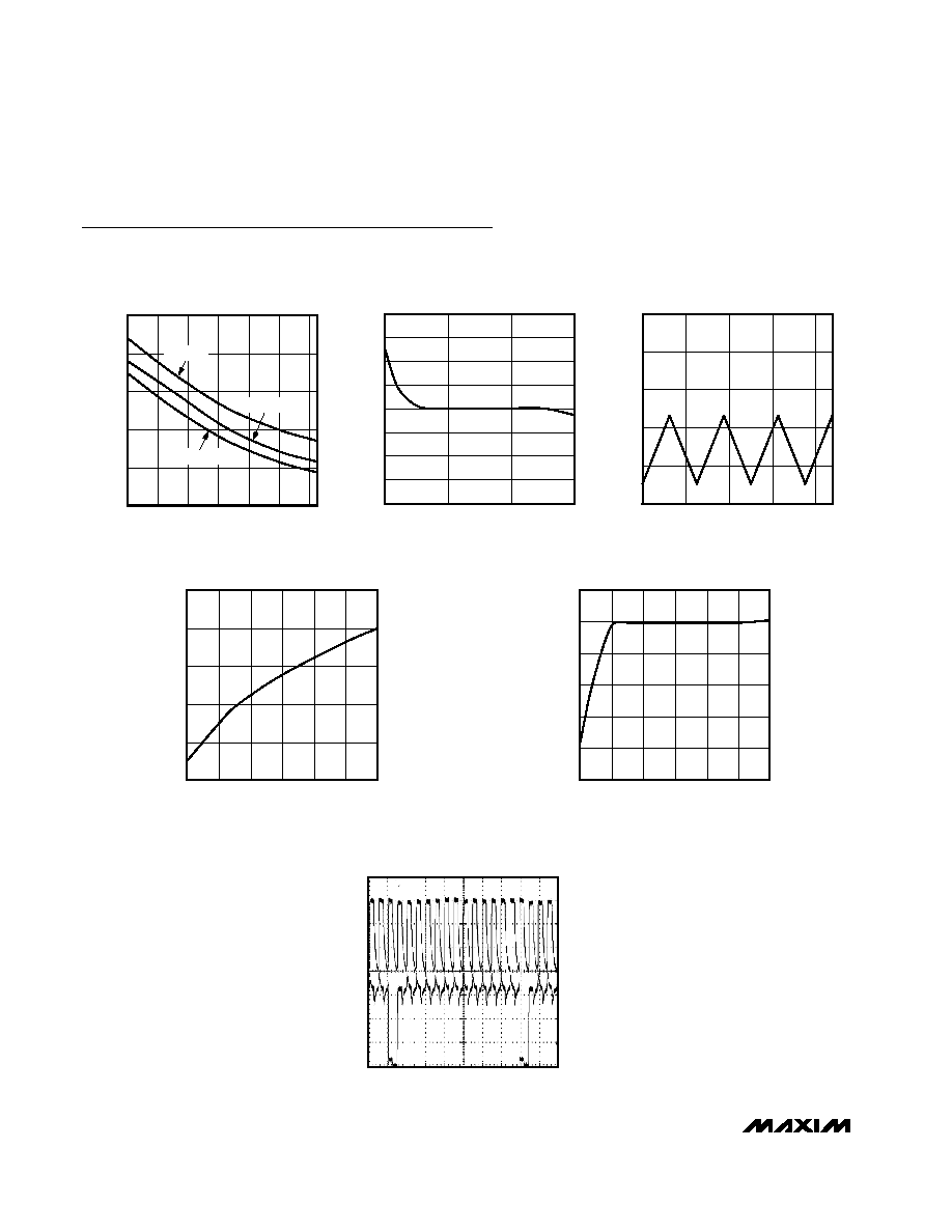
Typical Operating Characteristics
(Typical application circuit, V+ = 3.3V, LED forward voltage = 2.4V, scan limit set to 4 digits, T
A
= +25∞C, unless otherwise noted.)
3.80
3.90
4.10
4.00
4.20
4.30
-40
0
-20
20
40
60
80
INTERNAL OSCILLATOR
FREQUENCY vs. TEMPERATURE
MAX6952 toc01
TEMPERATURE (
∞C)
OSCILLATOR FREQUENCY (MHz)
V+ = 3.3V
V+ = 2.7V
V+ = 5V
INTERNAL OSCILLATOR FREQUENCY
vs. SUPPLY VOLTAGE
MAX6952 toc02
SUPPLY VOLTAGE (V)
OSCILLATOR FREQUENCY (MHz)
4.5
3.5
3.7
3.8
3.9
4.0
4.1
4.2
4.3
4.4
3.6
2.5
5.5
0
0.5
1.5
1.0
2.0
2.5
0
400
200
600
800
INTERNAL OSCILLATOR
WAVEFORM AT OSC
MAX6952 toc03
TIMELINE (ns)
VOLTAGE AT OSC (V)
80
85
95
90
100
105
2.5
3.5
3.0
4.0
4.5
5.0
5.5
DEAD CLOCK OSCILLATOR FREQUENCY
vs. SUPPLY VOLTAGE
MAX6952 toc04
SUPPLY VOLTAGE (V)
OSCILLATOR FREQUENCY (kHz)
0.95
0.97
0.96
0.99
0.98
1.00
1.01
2.5
3.5
4.0
3.0
4.5
5.0
5.5
SEGMENT SOURCE CURRENT
vs. SUPPLY VOLTAGE
MAX6952 toc05
SUPPLY VOLTAGE (V)
CURRENT NORMALIZED TO 40mA
WAVEFORMS AT O2 (PIN 3) AND O14
(PIN 28) 15/16 INTENSITY
GROUND FOR
ANODE
(PIN O14)
MAX6952 toc06
GROUND FOR
CATHODE
(PIN O3)
220
ms/div
Detailed Description
The MAX6952 is a serially interfaced display driver that
can drive four digits of 5
7 cathode-row dot-matrix
displays. The MAX6952 can drive either four monocolor
digits (Table 1) or two bicolor digits (Table 2). The
MAX6952 includes a 128-character font map compris-
ing 104 predefined characters and 24 user-definable
characters. The predefined characters follow the Arial
font, with the addition of the following common sym-
bols: £,
, •, ∞, µ, ±, , and . The 24 user-definable
characters are uploaded by the user into on-chip RAM
through the serial interface and are lost when the
device is powered down. Figure 1 is the MAX6952
functional diagram.
Serial Interface
The MAX6952 communicates through an SPI-compati-
ble 4-wire serial interface. The interface has three
inputs, clock (CLK), chip select (CS), and data in (DIN),
and one output, data out (DOUT). CS must be low to
clock data into or out of the device, and DIN must be
stable when sampled on the rising edge of CLK. DOUT
is stable on the rising edge of CLK. Note that while the
SPI protocol expects DOUT to be high impedance
when the MAX6952 is not being accessed, DOUT on
the MAX6952 is never high impedance.
MAX6952
4-Wire Interfaced, 2.7V to 5.5V,
4-Digit 5
7 Matrix LED Display Driver
_______________________________________________________________________________________
5
Pin Description
PIN
SSOP
PDIP
NAME
FUNCTION
1, 2, 3, 6≠14, 23, 24
1, 2, 3, 7≠15, 26, 27
O0 to O13
LED Cathode Drivers. O0 to O13 outputs sink current from
the display's cathode rows.
4, 5, 16
4, 5, 6, 18
GND
Ground
15
17
ISET
Segment Current Setting. Connect ISET to GND through
series resistor R
SET
to set the peak current.
17
19
BLINK
Blink Clock Output. Output is open drain.
18
20
DIN
Serial Data Input. Data is loaded into the internal 16-bit shift
register on the rising edge of the CLK.
19
21
CLK
Serial-Clock Input. On the rising edge of CLK, data is
shifted into the internal shift register. On the falling edge of
CLK, data is clocked out of DOUT. CLK input is active only
while CS is low.
20
22
DOUT
Serial Data Output. Data clocked into DIN is output to
DOUT 15.5 clock cycles later. Data is clocked out on the
rising edge of CLK. Output is push-pull.
21
23
CS
Chip-Select Input. Serial data is loaded into the shift register
while CS is low. The last 16 bits of serial data are latched on
CS's rising edge.
22
24
OSC
Multiplex Clock Input. To use the internal oscillator, connect
capacitor C
SET
from OSC to GND. To use the external
clock, drive OSC with a 1MHz to 8MHz CMOS clock.
25≠31, 34, 35, 36
28≠34, 38, 39, 40
O14 to O23
LED Anode Drivers. O14 to O23 outputs source current to
the display's anode columns.
32, 33
35, 36, 37
V+
Positive Supply Voltage. Bypass V+ to GND with a 47µF
bulk capacitor and a 0.1µF ceramic capacitor.