General Description
The MAX6966/MAX6967 serial-interfaced peripherals
provide microprocessors with 10 I/O ports rated to 7V.
Each port can be individually configured as either:
∑ A 20mA constant-current LED driver (static or pulse-
width modulated (PWM)).
∑ A 10mA constant-current LED driver (static or PWM).
∑ An open-drain logic output.
∑ An overvoltage-protected Schmitt logic input.
Analog and switching LED intensity control is built in:
∑ Individual 8-bit PWM control per output.
∑ Individual 1-bit analog control (half/full) per output.
∑ Global 3-bit analog control applies to all LED outputs.
PWM timing of the 10 port outputs may be optionally
staggered, consecutively phased in 45∞ increments.
This spreads the PWM load currents over time in eight
steps, helping to even out the power-supply current
and reduce the RMS current.
The MAX6966/MAX6967 can be configured to awake
from shutdown on receipt of a minimum 3ms pulse on
the CS input. This hardware-wakeup feature allows a
power-management controller or similar ASIC to enable
the MAX6966/MAX6967 with preconfigured LED intensi-
ty settings.
Shutdown can be programmed to wait up to 4s, fade
down the sink currents to zero for a period of 1/16s to
4s, and then shut down. A similar ramp-up from shut-
down can be programmed for 1/16s to 4s.
The MAX6966/MAX6967 support hot insertion. All port
pins remain high impedance in power-down (V+ = 0V)
with up to 8V asserted on them.
The DOUT/OSC pin can be configured as either the
serial interface data output or optional PWM clock
input. The MAX6966 powers up defaulting as DOUT
output. The MAX6967 defaults as OSC input.
For a similar part without the constant-current controls,
refer to the MAX7317 data sheet.
Applications
LCD Backlights
RGB LED Drivers
Keypad Backlights
Portable Equipment
LED Status Indication
Cellular Phones
Features
High-Speed 26MHz SPI-TM/QSPI-TM/MICROWIRETM-
Compatible Serial Interface
2.25V to 3.6V Operation
I/O Ports Default to High-Z (LEDs Off) on Power-Up
I/O Port Inputs Are Overvoltage Protected to 7V
I/O Port Outputs Are 7V-Rated Open Drain
I/O Port Outputs Are 10mA or 20mA Constant-
Current Static/PWM LED Drivers, or Open-Drain
Logic Outputs
I/O Ports Support Hot Insertion
Individual 8-Bit PWM Intensity Control for Each LED
Any Output May Use or Not Use PWM Control
Exit Shutdown (Warm Start) with Simple CS Pulse
Auto Ramp-Down into Shutdown
Auto Ramp-Up Out from Shutdown
0.8µA (typ), 2µA (max) Shutdown Current
Tiny 3mm x 3mm, 0.8mm High Thin QFN Package
-40∞C to +125∞C Temperature Range
MAX6966/MAX6967
10-Port Constant-Current LED Drivers and I/O
Expanders with PWM Intensity Control
________________________________________________________________ Maxim Integrated Products
1
Ordering Information
19-3487; Rev 2; 4/05
For pricing, delivery, and ordering information, please contact Maxim/Dallas Direct! at
1-888-629-4642, or visit Maxim's website at www.maxim-ic.com.
PART
TEMP
RANGE
PIN-
PACKAGE
TOP
MARK
PKG
CODE
MAX6966ATE
-40
∞C to
+125
∞C
16 Thin QFN
3mm x 3mm x
0.8mm
ACF
T1633-4
MAX6966AEE
-40
∞C to
+125
∞C
16 QSOP
--
--
MAX6967ATE
-40
∞C to
+125
∞C
16 Thin QFN
3mm x 3mm x
0.8mm
ACG
T1633-4
MAX6967AEE
-40
∞C to
+125
∞C
16 QSOP
--
--
SPI and QSPI are trademarks of Motorola, Inc.
MICROWIRE is a trademark of National Semiconductor Corp.
MAX6966/MAX6967
10-Port Constant-Current LED Drivers and I/O
Expanders with PWM Intensity Control
2
_______________________________________________________________________________________
ABSOLUTE MAXIMUM RATINGS
Stresses beyond those listed under "Absolute Maximum Ratings" may cause permanent damage to the device. These are stress ratings only, and functional
operation of the device at these or any other conditions beyond those indicated in the operational sections of the specifications is not implied. Exposure to
absolute maximum rating conditions for extended periods may affect device reliability.
Voltage (with respect to GND)
V+ .............................................................................-0.3V to +4V
SCLK, DIN, CS, DOUT/OSC.........................-0.3V to (V+ + 0.3V)
P_ .............................................................................-0.3V to +8V
DC Current into P_ .............................................................24mA
DC Current into DOUT/OSC................................................10mA
Total GND Current ............................................................280mA
Continuous Power Dissipation
16-Pin QSOP (derate 8.3mW/∞C over T
A
= +70∞C) ....667mW
16-Pin QFN (derate 14.7mW/∞C over T
A
= +70∞C) ...1176mW
Operating Temperature Range (T
MIN
to T
MAX
) .-40∞C to +125∞C
Junction Temperature ......................................................+150∞C
Storage Temperature Range .............................-65∞C to +150∞C
Lead Temperature (soldering, 10s) .................................+300∞C
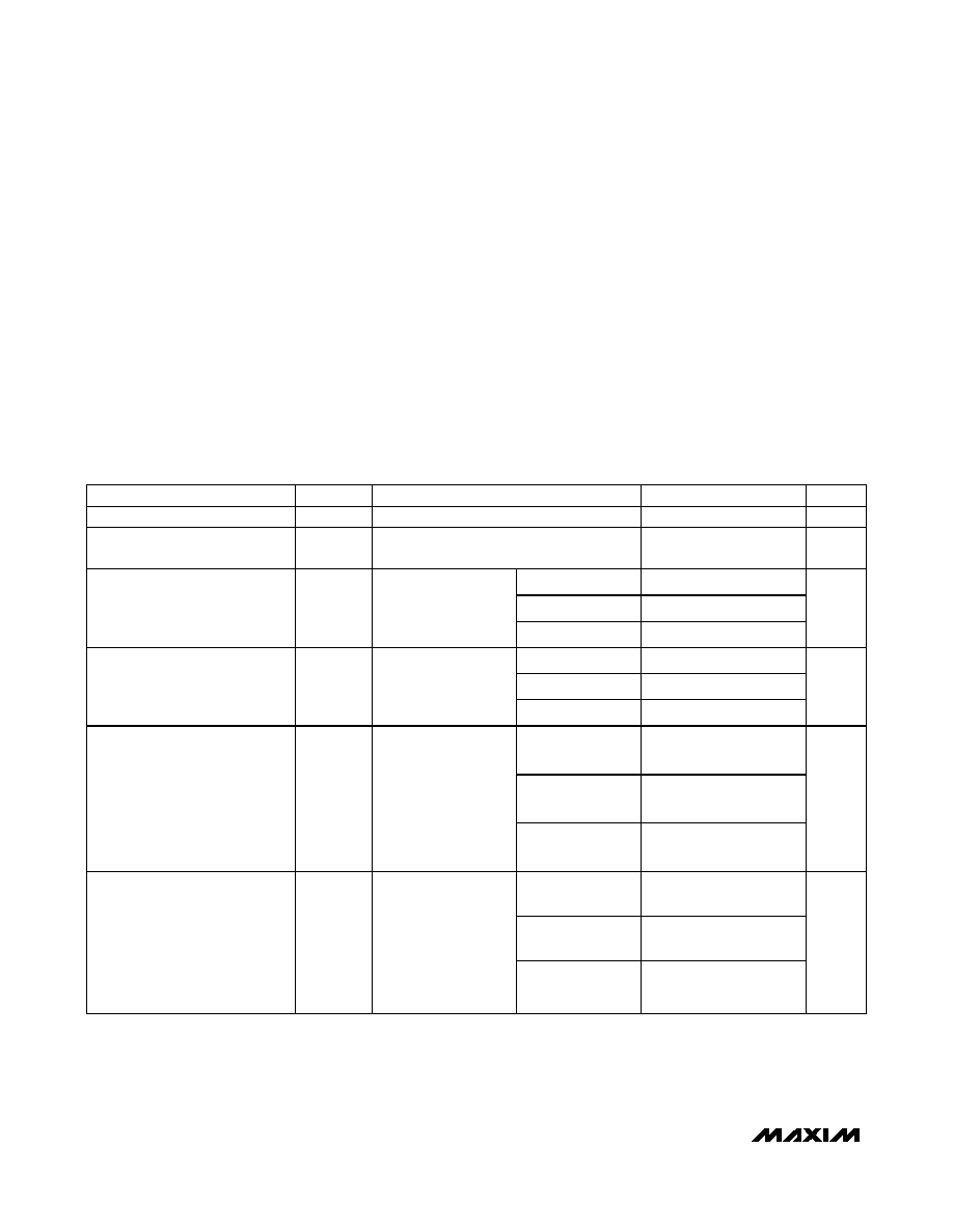
ELECTRICAL CHARACTERISTICS
(Typical Operating Circuit, V+ = 2.25V to 3.6V, T
A
= T
MIN
to T
MAX
, unless otherwise noted. Typical values are at V+ = 3.3V, T
A
=
+25∞C.) (Note 1)
PARAMETER
SYMBOL
CONDITIONS
MIN
TYP
MAX
UNITS
Operating Supply Voltage
V+
2.25
3.60
V
Output Load External Supply
Voltage P0≠P9
V
EXT
7
V
T
A
= +25∞C
0.7
1.5
T
A
= T
MIN
to +85∞C
1.7
Standby Current
(Interface Idle, CS Run Disabled,
PWM Disabled, All Ports High
Impedance)
I
STBY
CS at V+; other digital
inputs at V+ or GND
T
A
= T
MIN
to T
MAX
1.9
µA
T
A
= +25∞C
390
620
T
A
= T
MIN
to +85∞C
680
Supply-Current Interface Only
(CS Run Enabled, PWM
Disabled, All Ports High
Impedance)
I
+
f
SCLK
= 26MHz, other
digital inputs at V+ or
GND; DOUT unloaded
T
A
= T
MIN
to T
MAX
730
µA
T
A
= +25∞C
1.58
1.8
T
A
= T
MIN
to +85∞C
1.9
Delta Supply Current per 10mA
Port (Interface Idle, Global
Current Register Set to 0x07, One
Port's Output Register Set to
0x02 and Its Output Current
Register Bit Cleared; All Other
Ports' Output Registers Set to
0x00, 0x01, or 0xFF)
I
+10
Digital inputs at V+ or
GND
T
A
= T
MIN
to T
MAX
2
mA
T
A
= +25∞C
3.2
3.6
T
A
= T
MIN
to +85∞C
3.8
Delta Supply Current per 20mA
Port
( Inter face Id l e, Gl ob al C ur r ent
Reg i ster S et to 0x07, One P or t' s
Outp ut Reg i ster S et to 0x02 and Its
Outp ut C ur r ent Reg i ster Bi t S et; Al l
Other P or ts' Outp ut Reg i ster s S et to
0x00, 0x01, or 0xFF)
I
+20
Digital inputs at V+ or
GND
T
A
= T
MIN
to T
MAX
4.0
mA
MAX6966/MAX6967
10-Port Constant-Current LED Drivers and I/O
Expanders with PWM Intensity Control
_______________________________________________________________________________________
3
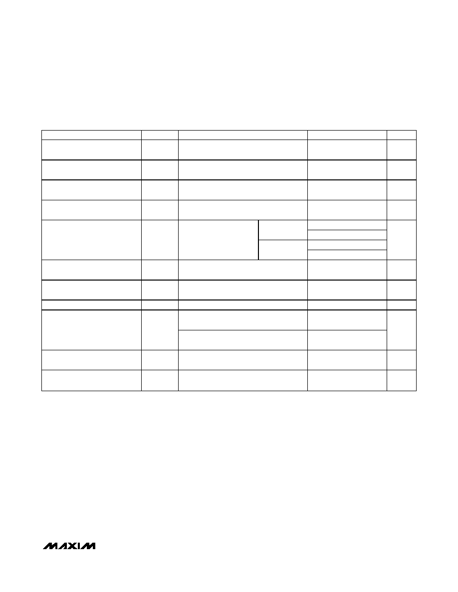
ELECTRICAL CHARACTERISTICS (continued)
(Typical Operating Circuit, V+ = 2.25V to 3.6V, T
A
= T
MIN
to T
MAX
, unless otherwise noted. Typical values are at V+ = 3.3V, T
A
=
+25∞C.) (Note 1)
PARAMETER
SYMBOL
CONDITIONS
MIN
TYP
MAX
UNITS
Input High Voltage
(P0≠P9, DIN, SCLK, CS, OSC)
V
IH
P0≠P9: output register set to 0x01
0.7 x
V+
V
Input Low Voltage
(P0≠P9, DIN, SCLK, CS, OSC)
V
IL
P0≠P9: output register set to 0x01
0.3 x
V+
V
Input Leakage Current
(P0≠P9, DIN, SCLK, CS, OSC)
I
IH
, I
IL
-0.2
+0.2
µA
Input Capacitance
(P0≠P9, DIN, SCLK, CS, OSC)
(Note 2)
10
pF
19.3
20
21.1
T
A
= +25∞C
9.5
10
10.7
18.8
21.8
Port Nominal Sink Constant
Current
(P0≠P9) (Global Current Register
Set to 0x07)
I
OUT
Output register set to
0x02,
V+ = 3.3V, V
EXT
- V
LED
=
1V to 2.5V (Note 3)
T
A
= T
MIN
to
+85∞C
9.1
11.0
mA
Port Logic Output Low Voltage
(P0≠P9)
V
OLP_
Output register set to 0x00,
I
SINK
= 0.5mA
0.4
V
Port Logic Output Low Short-
Circuit Current (P0≠P9)
Output register set to 0x00,
V
OLP_
= 5V
10.8
20
mA
Port Slew Time
From 20% current to 80% current
2
µs
T
A
= +25∞C, V+ = 3.3V, V
EXT
- V
LED
= 1.4V,
I
OUT
= 20mA
±1.5
±4
Port Sink Constant-Current
Matching
I
OUT
T
A
= +25∞C, V+ = 3.3V, V
EXT
- V
LED
= 1.4V,
I
OUT
= 10mA
±2
±5
%
Output High Voltage
(DOUT)
V
OHDOUT
I
SOURCE
= 6mA
V+ -
0.3V
V
Output Low Voltage
(DOUT)
V
OLDOUT
I
SINK
= 6mA
0.3
V
MAX6966/MAX6967
10-Port Constant-Current LED Drivers and I/O
Expanders with PWM Intensity Control
4
_______________________________________________________________________________________
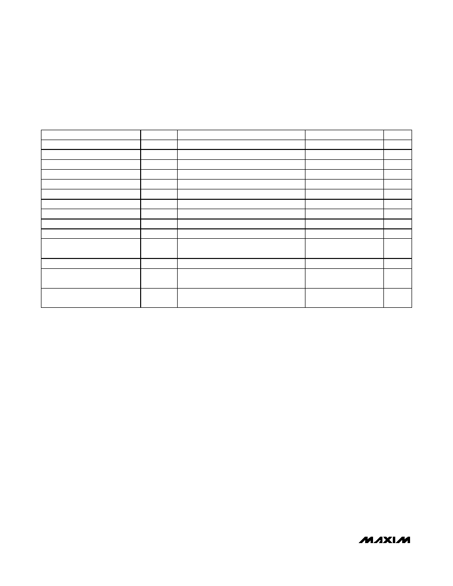
TIMING CHARACTERISTICS
(Typical Operating Circuit, V+ = 2.25V to 3.6V, T
A
= T
MIN
to T
MAX
, unless otherwise noted. Typical values are at V+ = 3.3V, T
A
=
+25∞C.) (Note 1)
PARAMETER
SYMBOL
CONDITIONS
MIN
TYP
MAX
UNITS
Internal PWM Clock Frequency
f
INT
27000
45000
Hz
External PWM Clock Frequency
f
OSC
100
kHz
SCLK Clock Period
t
CP
38.4
ns
SCLK Pulse Width High
t
CH
19
ns
SCLK Pulse Width Low
t
CL
19
ns
CS Fall to SCLK Rise Setup Time
t
CSS
9.5
ns
SCLK Rise to CS Rise Hold Time
t
CSH
0
ns
DIN Setup Time
t
DS
9.5
ns
DIN Hold Time
t
DH
0
ns
Output Data Propagation Delay
t
DO
21
ns
DOUT Output Rise and Fall
Times
t
FT
C
LOAD
= 20pF
10
ns
Minimum CS Pulse High
t
CSW
38.4
ns
CS Pulse Low to Not Activate CS
Run
t
CSRUN
CS run enabled
640
µs
CS Pulse Width to Activate CS
Run
t
CSRUN
CS run enabled
3
ms
Note 1: All parameters tested at T
A
= +25∞C. Specifications over temperature are guaranteed by design.
Note 2: Guaranteed by design.
Note 3: Port current is factory trimmed to meet a median sink current of 20mA and 10mA over all 10 ports. The
I
OUT
specification
guarantees current matching between ports.
Typical Operating Characteristics
(T
A
= +25∞C, unless otherwise noted.)
MAX6966/MAX6967
10-Port Constant-Current LED Drivers and I/O
Expanders with PWM Intensity Control
_______________________________________________________________________________________
5
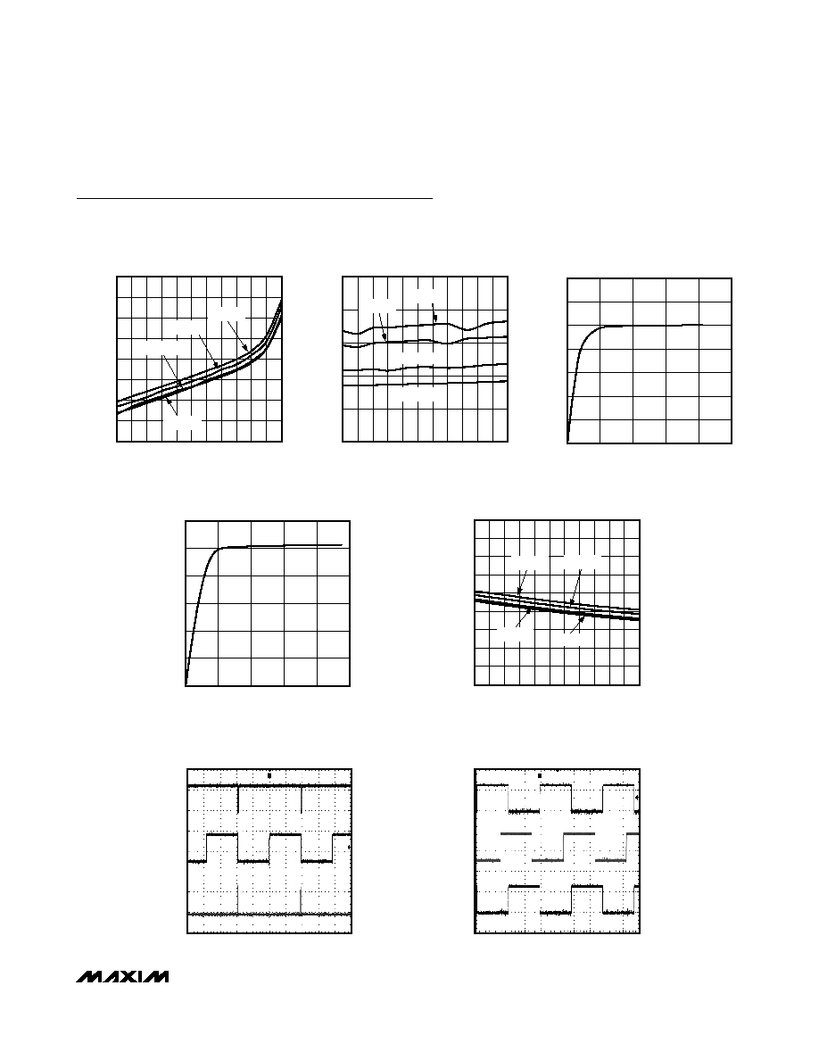
STANDBY CURRENT (I
STBY1
)
vs. TEMPERATURE
MAX6966/67 toc01
TEMPERATURE (
∞C)
STANDBY CURRENT (
µ
A)
110
95
-25 -10 5
35 50 65
20
80
0.5
0.6
0.7
0.8
0.9
1.0
1.1
1.2
0.4
-40
125
V+ = 3.6V
V+ = 3.3V
V+ = 2.7V
V+ = 2.25V
SUPPLY CURRENT (I+)
vs. TEMPERATURE
MAX6966/67 toc02
TEMPERATURE (
∞C)
SUPPLY CURRENT (mA)
110
95
80
65
50
35
20
5
-10
-25
0.1
0.2
0.3
0.4
0.5
0
-40
125
V+ = 3.6V
V+ = 3.3V
V+ = 2.7V
V+ = 2.25V
OUTPUT SINKING CURRENT
vs. V
EXT
- V
LED
AT 10mA
MAX6966/67 toc03
V
EXT
- V
LED
(V)
OUTPUT SINKING CURRENT (mA)
4
3
2
1
2
4
6
8
10
12
14
0
0
5
OUTPUT SINKING CURRENT
vs. V
EXT
- V
LED
AT 20mA
MAX6966/67 toc04
V
EXT
- V
LED
(V)
OUTPUT SINKING CURRENT (mA)
4
3
2
1
4
8
12
16
20
24
0
0
5
INTERNAL OSCILLATOR FREQUENCY
vs. TEMPERATURE
MAX6966/67 toc05
TEMPERATURE (
∞C)
FREQUENCY (kHz)
110
95
65 80
-10 5
20 35 50
-25
29
31
33
35
37
39
41
43
45
27
-40
125
V+ = 3.6V
V+ = 3.3V
V+ = 2.7V
V+ = 2.25V
SAMPLE PWM WAVEFORMS
2ms
OUTPUT
REGISTER
= 0x03
OUTPUT
REGISTER
= 0x80
OUTPUT
REGISTER
= 0xFE
MAX6966/67 toc06
STAGGER PWM PORT WAVEFORMS
(OUTPUT REGISTERS SET TO 0x80)
2ms
PORT P4
PORT P0
PORT P1
MAX6966/67 toc07