 | –≠–ª–µ–∫—Ç—Ä–æ–Ω–Ω—ã–π –∫–æ–º–ø–æ–Ω–µ–Ω—Ç: MAX712CSE | –°–∫–∞—á–∞—Ç—å:  PDF PDF  ZIP ZIP |

_______________General Description
The MAX712/MAX713 fast charge Nickel Metal Hydride
(NiMH) and Nickel Cadmium (NiCd) batteries from a DC
source at least 1.5V higher than the maximum battery
voltage. 1 to 16 series cells can be charged at rates up
to 4C. A voltage-slope detecting analog-to-digital convert-
er, timer, and temperature window comparator determine
charge completion. The MAX712/MAX713 are powered
by the DC source via an on-board +5V shunt regulator.
They draw a maximum of 5
µ
A from the battery when not
charging. A low-side current-sense resistor allows the
battery charge current to be regulated while still
supplying power to the battery's load.
The MAX712 terminates fast charge by detecting zero
voltage slope, while the MAX713 uses a negative
voltage-slope detection scheme. Both parts come in 16-
pin DIP and SO packages. An external power PNP tran-
sistor, blocking diode, three resistors, and three
capacitors are the only required external components.
For high-power charging requirements, the MAX712/
MAX713 can be configured as a switch-mode battery
charger that minimizes power dissipation. Two evaluation
kits are available: Order the MAX712EVKIT-DIP for quick
evaluation of the linear charger, and the MAX713EVKIT-
SO to evaluate the switch-mode charger.
________________________Applications
Battery-Powered Equipment
Laptop, Notebook, and Palmtop Computers
Handy-Terminals
Cellular Phones
Portable Consumer Products
Portable Stereos
Cordless Phones
____________________________Features
o
Fast Charge NiMH or NiCd Batteries
o
Voltage Slope, Temperature, and Timer
Fast-Charge Cutoff
o
Charge 1 to 16 Series Cells
o
Supply Battery's Load while Charging (Linear Mode)
o
Fast Charge from C/4 to 4C Rate
o
C/16 Trickle-Charge Rate
o
Automatically Switch from Fast to Trickle Charge
o
Linear or Switch-Mode Power Control
o
5µA Max Drain on Battery when Not Charging
o
5V Shunt Regulator Powers External Logic
MAX712/MAX713
NiCd/NiMH Battery
Fast-Charge Controllers
________________________________________________________________
Maxim Integrated Products
1
MAX712
MAX713
THI
R2
150
R3
68k
R4
22k
R1
10
µ
F
C4
0.01
µ
F
C1
1
µ
F
C3
10
µ
F
C2
0.01
µ
F
DRV
Q1
2N6109
DC IN
WALL
CUBE
SEE FIGURE 19 FOR SWITCH-MODE CHARGER CIRCUIT.
D1
1N4001
BATTERY
R
SENSE
V+
VLIMIT
BATT+
REF
TEMP
BATT- TLO GND
CC
LOAD
__________Typical Operating Circuit
16
15
14
13
12
11
10
9
1
2
3
4
5
6
7
8
REF
V+
DRV
GND
BATT-
CC
PGM3
PGM2
VLIMIT
BATT+
PGM0
PGM1
THI
TLO
TEMP
FASTCHG
TOP VIEW
MAX712
MAX713
DIP/SO
__________________Pin Configuration
19-0100; Rev 3; 1/97
PART
MAX712
CPE
MAX712CSE
MAX712C/D
0∞C to +70∞C
0∞C to +70∞C
0∞C to +70∞C
TEMP. RANGE
PIN-PACKAGE
16 Plastic DIP
16 Narrow SO
Dice*
EVALUATION KIT MANUALS
FOLLOW DATA SHEET
______________Ordering Information
Ordering Information continued at end of data sheet.
*
Contact factory for dice specifications.
**
Contact factory for availability and processing to MIL-STD-883.
For free samples & the latest literature: http://www.maxim-ic.com, or phone 1-800-998-8800
MAX712EPE
MAX712ESE
MAX712MJE
-55∞C to +125∞C
-40∞C to +85∞C
-40∞C to +85∞C
16 Plastic DIP
16 Narrow SO
16 CERDIP**
MAX712/MAX713
NiCd/NiMH Battery
Fast-Charge Controllers
2
_______________________________________________________________________________________
ABSOLUTE MAXIMUM RATINGS
ELECTRICAL CHARACTERISTICS
(I
V+
= 10mA, T
A
= T
MIN
to T
MAX
, unless otherwise noted. Refer to
Typical Operating Circuit. All measurements are with respect to
BATT-, not GND.)
Stresses beyond those listed under "Absolute Maximum Ratings" may cause permanent damage to the device. These are stress ratings only, and functional
operation of the device at these or any other conditions beyond those indicated in the operational sections of the specifications is not implied. Exposure to
absolute maximum rating conditions for extended periods may affect device reliability.
V+ to BATT- .................................................................-0.3V, +7V
BATT- to GND ........................................................................±1V
BATT+ to BATT-
Power Not Applied............................................................±20V
With Power Applied ................................The higher of ±20V or
±2V x (programmed cells)
DRV to GND ..............................................................-0.3V, +20V
FASTCHG to BATT- ...................................................-0.3V, +12V
All Other Pins to GND......................................-0.3V, (V+ + 0.3V)
V+ Current.........................................................................100mA
DRV Current. .....................................................................100mA
REF Current.........................................................................10mA
Continuous Power Dissipation (T
A
= +70∞C)
Plastic DIP (derate 10.53mW/∞C above +70∞C............842mW
Narrow SO (derate 8.70mW/∞C above +70∞C .............696mW
CERDIP (derate 10.00mW/∞C above +70∞C ................800mW
Operating Temperature Ranges
MAX71_C_E .......................................................0∞C to +70∞C
MAX71_E_E .................................................... -40∞C to +85∞C
MAX71_MJE ................................................. -55∞C to +125∞C
Storage Temperature Range .............................-65∞C to +150∞C
Lead Temperature (soldering, 10sec) .............................+300∞C
V
DRV
= 10V
V+ = 0V, BATT+ = 17V
PGM3 = BATT-
5mA < I
V+
< 20mA
PGM3 = REF
PGM3 = open
PGM3 = V+
0V < TEMP < 2V, TEMP voltage rising
V
LIMIT
= V+
Per cell
PGM0 = PGM1 = BATT-, BATT+ = 30V
1.2V < V
LIMIT
< 2.5V, 5mA < I
DRV
< 20mA,
PGM0 = PGM1 = V+
0mA < I
REF
< 1mA
CONDITIONS
mA
30
DRV Sink Current
%
-1.5
1.5
Battery-Voltage to Cell-Voltage
Divider Accuracy
%
-15
15
Timer Accuracy
mV
26.0
31.3
38.0
Trickle-Charge VSENSE
12.0
15.6
20.0
4.5
7.8
12.0
1.5
3.9
7.0
mV
225
250
275
Fast-Charge VSENSE
V
1.6
1.65
1.7
Internal Cell Voltage Limit
mV
-30
30
VLIMIT Accuracy
µA
-1
1
THI, TLO, TEMP, VLIMIT Input Bias Current
µA
5
BATT+ Leakage
mA
5
I
V+
(Note 1)
V
4.5
5.5
V+ Voltage
mV
-10
10
THI, TLO Offset Voltage (Note 2)
V
0
2
THI, TLO, TEMP Input Range
V
1.25
2.50
External VLIMIT Input Range
V
0.35
0.50
Undervoltage Lockout
k
30
BATT+ Resistance with Power On
µF
0.5
C1 Capacitance
nF
5
C2 Capacitance
V
1.96
2.04
REF Voltage
UNITS
MIN
TYP
MAX
PARAMETER
MAX712
MAX713
mV/t
A
per cell
0
Voltage-Slope Sensitivity (Note 3)
-2.5

ELECTRICAL CHARACTERISTICS (continued)
(I
V
+ = 10mA, T
A
= T
MIN
to T
MAX
, unless otherwise noted. Refer to
Typical Operating Circuit. All measurements are with respect to
BATT-, not GND.)
Note 1:
The MAX712/MAX713 are powered from the V+ pin. Since V+ shunt regulates to +5V, R1 must be small enough to allow at
least 5mA of current into the V+ pin.
Note 2:
Offset voltage of THI and TLO comparators referred to TEMP.
Note 3:
t
A
is the A/D sampling interval (Table 3).
Note 4:
This specification can be violated when attempting to charge more or fewer cells than the number programmed. To ensure
proper voltage-slope fast-charge termination, the (maximum battery voltage) ˜ (number of cells programmed) must fall
within the A/D input range.
MAX712/MAX713
NiCd/NiMH Battery
Fast-Charge Controllers
_______________________________________________________________________________________
3
Battery voltage ˜ number of cells programmed
V
FASTCHG
= 10V
V
FASTCHG
= 0.4V
CONDITIONS
V
1.4
1.9
A/D Input Range (Note 4)
µA
10
FASTCHG High Current
mA
2
FASTCHG Low Current
UNITS
MIN
TYP
MAX
PARAMETER
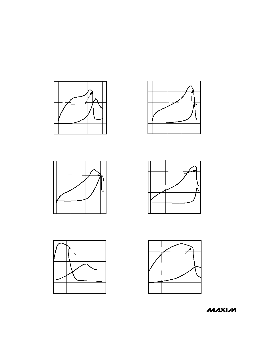
__________________________________________Typical Operating Characteristics
(T
A
= +25∞C, unless otherwise noted.)
20
1k
100k
1M
10k
10M
CURRENT-SENSE AMPLIFIER
FREQUENCY RESPONSE (with 15pF)
-20
FREQUENCY (Hz)
GAIN (dB)
PHASE (DEGREES)
-10
0
10
40
-120
-80
-40
0
C2 = 15pF
FASTCHG = 0V
V
OUT
V
IN
CURRENT-
SENSE
AMP
BATT-
BATT-
CC
GND
-
-
+
+
MAX712/13 LOG1
A
V
20
-10
-20
10
1k
CURRENT-SENSE AMPLIFIER
FREQUENCY RESPONSE (with 10nF)
0
10
40
-80
-120
-40
0
FREQUENCY (Hz)
GAIN (dB)
PHASE (DEGREES)
100
10k
C2 = 10nF
FASTCHG = 0V
MAX712/13 LOG2
A
V
100
0.1
1.95
1.97
2.01
2.05
CURRENT ERROR-AMPLIFIER
TRANSCONDUCTANCE
1
10
VOLTAGE ON CC PIN (V)
DRV PIN SINK CURRENT(mA)
1.99
2.03
FASTCHG = 0V, V+ = 5V
MAX712/13 LOG3
5.8
4.8
0
60
SHUNT-REGULATOR VOLTAGE
vs. CURRENT
5.6
CURRENT INTO V+ PIN (mA)
V+ VOLTAGE (V)
30
5.2
5.0
10
20
50
5.4
4.0
4.4
4.2
4.6
40
DRV NOT SINKING CURRENT
DRV SINKING CURRENT
MAX712/13 LOG4
1.0
0
60
ALPHA THERMISTOR PART No. 13A1002
STEINHART-HART INTERPOLATION
1.6
BATTERY TEMPERATURE(
∞
C)
TEMP PIN VOLTAGE (V)
BATTERY THERMISTOR RESISTANCE (k
)
30
1.4
1.2
10
20
50
0.2
0.6
0.4
0.8
20
35
30
25
0
10
5
15
40
MAX712/MAX713
NiCd/NiMH Battery
Fast-Charge Controllers
4
_______________________________________________________________________________________
____________________________Typical Operating Characteristics (continued)
(T
A
= +25∞C, unless otherwise noted.)
1.45
0
MAX713
NiMH BATTERY-CHARGING
CHARACTERISTICS AT C RATE
1.50
CHARGE TIME (MINUTES)
CELL VOLTAGE (V)
CELL TEMPERATURE (
∞
C)
MAX712/713
1.60
1.55
25
30
40
35
30
90
60
V
t
CUTOFF
V
T
1.40
0
MAX713
NiCd BATTERY-CHARGING
CHARACTERISTICS AT C/2 RATE
1.45
CHARGE TIME (MINUTES)
CELL VOLTAGE (V)
CELL TEMPERATURE (
∞
C)
MAX712/713
1.50
25
30
35
50
150
100
V
t
CUTOFF
V
T
1.40
0
MAX713
NiMH BATTERY-CHARGING
CHARACTERISTICS AT C/2 RATE
1.45
CHARGE TIME (MINUTES)
CELL VOLTAGE (V)
CELL TEMPERATURE (
∞
C)
MAX712/713
1.55
1.50
25
30
40
35
50
150
100
V
t
CUTOFF
V
T
1.45
0
MAX713
CHARGING CHARACTERISTICS OF A
FULLY CHARGED NiMH BATTERY
1.50
CHARGE TIME (MINUTES)
CELL VOLTAGE (V)
CELL TEMPERATURE (
∞
C)
MAX712/713
1.60
1.65
1.55
25
30
40
35
5
15
20
10
5-MINUTE REST
BETWEEN CHARGES
V
t
CUTOFF
V
T
1.45
0
MAX713
CHARGING CHARACTERISTICS OF A
FULLY CHARGED NiMH BATTERY
1.50
CHARGE TIME (MINUTES)
CELL VOLTAGE (V)
CELL TEMPERATURE (
∞
C)
MAX712/713
1.60
1.65
1.55
25
30
40
35
5
15
10
5-HOUR REST
BETWEEN CHARGES
V
t
CUTOFF
V
T
20
1.40
0
MAX713
NiCd BATTERY-CHARGING
CHARACTERISTICS AT C RATE
1.45
CHARGE TIME (MINUTES)
CELL VOLTAGE (V)
CELL TEMPERATURE (
∞
C)
MAX712/713
1.55
1.50
25
30
40
35
30
90
60
V
t
CUTOFF
V
T
MAX712/MAX713
NiCd/NiMH Battery
Fast-Charge Controllers
_______________________________________________________________________________________
5
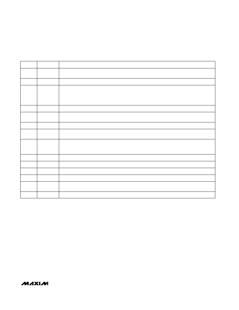
______________________________________________________________Pin Description
Compensation input for constant current regulation loop
CC
11
Negative terminal of battery
BATT-
12
System ground. The resistor placed between BATT- and GND monitors the current into the battery.
GND
13
Current sink for driving the external PNP current source
DRV
14
Shunt regulator. The voltage on V+ is regulated to +5V with respect to BATT-, and the shunt current
powers the MAX712/MAX713.
V+
15
Trip point for the under-temperature comparator. If the MAX712/MAX713 power on with the voltage-on
TEMP less than TLO, fast charge is inhibited and will not start until TEMP rises above TLO.
TLO
6
Sense input for temperature-dependent voltage from thermistors.
TEMP
7
Open-drain, fast-charge status output. While the MAX712/MAX713 fast charge the battery,
FASTCHG
sinks current. When charge ends and trickle charge begins,
FASTCHG stops sinking current.
FASTCHG
8
PGM2 and PGM3 set the maximum time allowed for fast charging. Timeouts from 33 minutes to 264
minutes can be set by connecting to any of V+, REF, or BATT-, or by leaving the pin open (Table 3).
PGM3 also sets the fast-charge to trickle-charge current ratio (Table 5).
PGM2,
PGM3
9, 10
Trip point for the over-temperature comparator. If the voltage-on TEMP rises above THI, fast charge ends.
THI
5
PGM0 and PGM1 set the number of series cells to be charged. The number of cells can be set from
1 to 16 by connecting PGM0 and PGM1 to any of V+, REF, or BATT-, or by leaving the pin open (Table
2). For cell counts greater than 11, see the
Linear-Mode, High Series Cell Count section. Charging more
or fewer cells than the number programmed may inhibit
V fast-charge termination.
PGM0,
PGM1
3, 4
PIN
Positive terminal of battery
BATT+
2
Sets the maximum cell voltage. The battery terminal voltage (BATT+ - BATT-) will not exceed VLIMIT x
(number of cells). Do not allow VLIMIT to exceed 2.5V. Tie VLIMIT to VREF for normal operation.
VLIMIT
1
FUNCTION
NAME
2V reference output
REF
16