Äîêóìåíòàöèÿ è îïèñàíèÿ www.docs.chipfind.ru
General Description
The MAX7382 silicon oscillator replaces ceramic res-
onators, crystals, and crystal-oscillator modules as the
clock source for microcontrollers in 3V, 3.3V, and 5V
applications. The MAX7382 features a factory-pro-
grammed oscillator and a microprocessor (µP) power-
on-reset (POR) supervisor.
Unlike typical crystal and ceramic-resonator oscillator
circuits, the MAX7382 is resistant to vibration and EMI.
The high-output-drive current and absence of high-
impedance nodes makes the oscillator less susceptible
to dirty or humid operating conditions. With a wide
operating temperature range as standard, the
MAX7382 is a good choice for demanding home appli-
ance and automotive environments.
The MAX7382 is available with factory-programmed fre-
quencies ranging from 10MHz to 32MHz. See Table 2
for standard frequencies and contact the factory for
custom frequencies. Refer to the MAX7376 data sheet
for frequencies less than 10MHz.
The MAX7382 is available in a 5-pin SOT23 package.
The MAX7382 standard operating temperature range is
-40°C to +125°C. See the Applications Information sec-
tion for extended operating temperature range.
Applications
White Goods
Automotive
Consumer Products
Appliances and Controls
Handheld Products
Portable Equipment
Microcontroller Systems
Features
2.7V to 5.5V Operation
10MHz to 32MHz Oscillator
Integrated POR
±10mA Clock Output Drive Capability
2.5% Initial Accuracy
±50ppm/°C Frequency Drift
50% Duty Cycle
5ns Output Rise and Fall Time
Low Jitter: 80ps
P-P
at 16MHz
4mA Operating Current at 16MHz
-40°C to +125°C Temperature Range
Small 5-Pin SOT23 Package
MAX7382
Silicon Oscillator with Reset Output
________________________________________________________________ Maxim Integrated Products
1
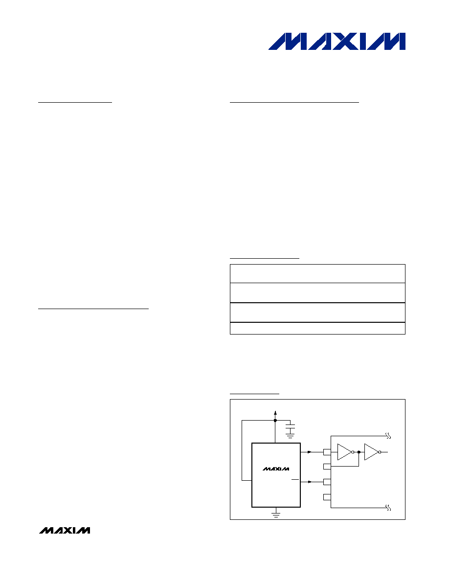
Ordering Information
OSC1
OSC2
RST
µC
GND
RST/RST
CLOCK
E.C.
V
CC
0.1
µF
V
CC
2.7V TO 5.5V
MAX7382
Typical Operating Circuit
19-3491; Rev 0; 1/05
For pricing, delivery, and ordering information, please contact Maxim/Dallas Direct! at
1-888-629-4642, or visit Maxim's website at www.maxim-ic.com.
PART*
TEMP RANGE
PIN-
PACKAGE
RESET
OUTPUT
MAX7382A_ _ _-T -40
°C to +125°C 5 SOT23-5
Active-high
push-pull
MAX7382B_ _ _-T -40
°C to +125°C 5 SOT23-5
Active-low
push-pull
MAX7382C_ _ _-T -40
°C to +125°C 5 SOT23-5 Open drain
*Standard version is shown in bold. The first letter after the part
number designates the reset output option. Insert the letter
corresponding to the desired reset threshold level from Table 1
in the next position. Insert the two-letter code from Table 2 in
the remaining two positions for the desired frequency range.
Table 1 and Table 2 are located at the end of the data sheet.
Pin Configuration appears at end of data sheet.

MAX7382
Silicon Oscillator with Reset Output
2
_______________________________________________________________________________________
ABSOLUTE MAXIMUM RATINGS
Stresses beyond those listed under "Absolute Maximum Ratings" may cause permanent damage to the device. These are stress ratings only, and functional
operation of the device at these or any other conditions beyond those indicated in the operational sections of the specifications is not implied. Exposure to
absolute maximum rating conditions for extended periods may affect device reliability.
V
CC
to GND ...........................................................-0.3V to +6.0V
All Other Pins to GND...................................-0.3V to (V+ + 0.3V)
CLOCK, RST Current .......................................................±50mA
Continuous Power Dissipation (T
A
= +70°C)
5-Pin SOT23 (derate 7.1mW/°C above +70°C) ....571mW (U5-2)
Operating Temperature Range .........................-55°C to +135°C
Junction Temperature ......................................................+150°C
Storage Temperature Range .............................-65°C to +150°C
Lead Temperature (soldering, 10s) .................................+300°C
ELECTRICAL CHARACTERISTICS
(Typical Operating Circuit, V
CC
= 2.7V to 5.5V, V
L
= V
CC
, T
A
= -40°C to +125°C. Typical values are at V
CC
= 5.0V, T
A
= +25°C,
unless otherwise noted.) (Note 1)
PARAMETER
SYMBOL
CONDITIONS
MIN
TYP
MAX
UNITS
Operating Supply Voltage
V
CC
2.7
5.5
V
f
CLOCK
= 16MHz, T
A
= -40°C to +125°C,
no load
8.7
f
CLOCK
= 14.7456MHz, T
A
= -40°C to
+125°C, no load
8.0
f
CLOCK
= 12MHz, T
A
= -40°C to +125°C,
no load
6.5
f
CLOCK
= 11.0592MHz, T
A
= -40°C to
+125°C, no load
6.0
Operating Supply Current
I
CC
f
CLOCK
= 10MHz, T
A
= -40°C to +125°C,
no load
5.4
mA
CLOCK OUTPUT
V
L
= 4.5V, I
SOURCE
= 7.0mA
Output High Voltage
V
OH
V
L
= 2.7V, I
SOURCE
= 2.0mA
V
L
- 0.4
V
V
L
= 4.5V, I
SINK
= 20mA
Output Low Voltage
V
OL
V
L
= 2.7V, I
SINK
= 10mA
0.4
V
V
CC
= 5V, T
A
= +25°C, deviation from
selected frequency
-2.5
+2.5
Clock Frequency Accuracy
f
CLOCK
V
CC
= 2.7V to 5.5V, T
A
= +25°C,
deviation from selected frequency
-5.0
+3.5
%
Clock Temperature Coefficient
T
A
= -40°C to +125°C
±50
±350
ppm/°C
Duty Cycle
(Note 2)
40
50
60
%
MAX7382
Silicon Oscillator with Reset Output
_______________________________________________________________________________________
3
ELECTRICAL CHARACTERISTICS (continued)
(Typical Operating Circuit, V
CC
= 2.7V to 5.5V, V
L
= V
CC
, T
A
= -40°C to +125°C. Typical values are at V
CC
= 5.0V, T
A
= +25°C,
unless otherwise noted.) (Note 1)
PARAMETER
SYMBOL
CONDITIONS
MIN
TYP
MAX
UNITS
Output Jitter
Observation of 16MHz for 20s using a
12GHz oscilloscope
80
ps
P-P
Output Rise Time
t
R
10% to 90%
5
ns
Output Fall Time
t
F
90% to 10%
5
ns
T
A
= +25°C
-2
+2
Power-On-Reset Threshold
V
TH
V
CC
rising, deviation
from nominal threshold
T
A
= -40°C to
+125°C
-5
+5
%
Reset Hysteresis
HYST
Difference between rising and falling
thresholds
1
%
Power-On-Reset Delay
POR
DLY
V
CC
rising from 0 to 5V in 1µs at +25
°C
122
µs
RESET OUTPUT
V
L
= 4.5V, I
SOURCE
= 7.0mA
V
CC
-
0.4
Output High Voltage
(Note 3)
V
OH
V
L
= 2.7V, I
SOURCE
= 2.0mA
V
CC
-
0.4
V
V
L
= 4.5V, I
SINK
= 20mA
0.4
Output Low Voltage
V
OL
V
L
= 2.7V, I
SOURCE
= 10mA
0.4
V
Note 1: All parameters tested at T
A
= +25°C. Specifications over temperature are guaranteed by design.
Note 2: Guaranteed by design. Not production tested.
Note 3: For push-pull output only.

MAX7382
Silicon Oscillator with Reset Output
4
_______________________________________________________________________________________
Typical Operating Characteristics
(V
CC
= V
L
= 5V, T
A
= +25°C, frequency = 10MHz, unless otherwise noted.)
48.0
48.5
49.5
49.0
50.0
50.5
-55
21
-17
59
97
135
DUTY CYCLE vs. TEMPERATURE
MAX7382 toc01
TEMPERATURE (
°C)
DUTY CYCLE (%)
FREQUENCY = 10MHz
DUTY CYCLE
vs. SUPPLY VOLTAGE
MAX7382 toc02
SUPPLY VOLTAGE (V)
DUTY CYCLE (%)
5.1
4.7
4.3
3.9
3.5
3.1
46
47
48
49
50
51
45
2.7
5.5
FREQUENCY = 11.0592MHz
2.90
3.00
2.95
3.10
3.05
3.20
3.15
3.25
-55
21
59
-17
97
135
SUPPLY CURRENT vs. TEMPERATURE
MAX7382 toc03
TEMPERATURE (
°C)
SUPPLY CURRENT (mA)
FREQUENCY = 10MHz
SUPPLY CURRENT vs. SUPPLY VOLTAGE
MAX7382 toc04
SUPPLY VOLTAGE (V)
SUPPLY CURRENT (mA)
5.1
4.7
4.3
3.9
3.5
3.1
2.0
2.5
3.0
3.5
4.0
1.5
2.7
5.5
FREQUENCY = 11.0592MHz
FREQUENCY DEVIATION
vs. SUPPLY VOLTAGE
MAX7382 toc05
SUPPLY VOLTAGE (V)
FREQUENCY DEVIATION (%)
5.1
4.7
3.1
3.5
3.9
4.3
-1.5
-1.0
-0.5
0
0.5
1.0
1.5
2.0
-2.0
2.7
5.5
FREQUENCY = 11.0592MHz
FREQUENCY DEVIATION
vs. TEMPERATURE
MAX7382 toc06
TEMPERATURE (
°C)
FREQUENCY DEVIATION (%)
97
59
-17
21
-3
-2
-1
0
1
2
3
4
-4
-55
135
FREQUENCY = 10MHz
CHANNEL 1 = CLOCK, CHANNEL 2 = V
CC
10
µs/div
SETTLING TIME FROM START
MAX7382 toc07
CH1 FREQ
9.992MHz
LOW RESOLUTION
CLOCK OUTPUT WAVEFORM
(C
L
= 10pF)
MAX7382 toc08
20ns/div
CLOCK OUTPUT WAVEFORM
(C
L
= 10pF)
MAX7382 toc09
20ns/div

MAX7382
Silicon Oscillator with Reset Output
_______________________________________________________________________________________
5
CLOCK OUTPUT WAVEFORM
(C
L
= 100pF)
MAX7382 toc10
20ns/div
MAXIMUM TRANSIENT DURATION
vs. RESET THRESHOLD OVERDRIVE
MAX7382 toc11
RESET THRESHOLD OVERDRIVE (V)
MAXIMUM TRANSIENT DURATION (s)
0.19
0.14
0.09
100m
10m
1m
0.01
0.1
1
1
µ
0.04
0.24
V
RESET
= 4.32V
SUPPLY CURRENT
vs. FREQUENCY
MAX7382 toc12
FREQUENCY (MHz)
SUPPLY CURRENT (mA)
15
14
13
12
11
2
3
4
5
1
10
16
Typical Operating Characteristics (continued)
(V
CC
= V
L
= 5V, T
A
= +25°C, frequency = 10MHz, unless otherwise noted.)
Pin Description
PIN
NAME
FUNCTION
1
CLOCK
Push-Pull Clock Output
2
GND
Ground
3
RST
Reset Output. Open-drain or push-pull output. See the Ordering Information.
4
V
CC
Positive Supply Voltage. Bypass with a 0.1µF capacitor to GND.
5
E.C.
Externally Connected. Connect to Vcc.
Detailed Description
The MAX7382 is a clock generator with integrated reset
for microcontrollers (µCs) and UARTs in 3V, 3.3V, and
5V applications. The MAX7382 is a replacement for
crystal-oscillator modules, crystals, or ceramic res-
onators, and a system reset IC. The clock frequency
and reset threshold voltage are factory trimmed to spe-
cific values. A variety of popular standard frequencies
are available; see Table 2. No external components are
required for setting or adjusting the frequency.
Oscillator
The push-pull clock output drives a load to within
400mV of either supply rail. The clock output remains
stable over the full operating voltage range and does
not generate short output cycles during either power-on
or changing of the frequency. A typical oscillating start-
up is shown in the Typical Operating Characteristics.