MAX807L/M/N
Full-Featured µP Supervisory Circuit with
±1.5% Reset Accuracy
________________________________________________________________ Maxim Integrated Products
1
19-0433; Rev 3; 4/03
General Description
The MAX807 microprocessor (µP) supervisory circuit
reduces the complexity and number of components
needed to monitor power-supply and battery-control func-
tions in µP systems. A 70µA supply current makes the
MAX807 ideal for use in portable equipment, while a 2ns
chip-enable propagation delay and 250mA output current
capability (20mA in battery-backup mode) make it suit-
able for larger, higher-performance equipment.
The MAX807 comes in 16-pin DIP, SO, and TSSOP pack-
ages, and provides the following functions:
∑ µP reset. The active-low RESET output is asserted dur-
ing power-up, power-down, and brownout conditions,
and is guaranteed to be in the correct state for V
CC
down to 1V.
∑ Active-high RESET output.
∑ Manual-reset input.
∑ Two-stage power-fail warning. A separate low-line
comparator compares V
CC
to a threshold 52mV above
the reset threshold. This low-line comparator is more
accurate than those in previous µP supervisors.
∑ Backup-battery switchover for CMOS RAM, real-time
clocks, µPs, or other low-power logic.
∑ Write protection of CMOS RAM or EEPROM.
∑ 2.275V threshold detector provides for power-fail
warning and low-battery detection, or monitors a
power supply other than +5V.
∑ BATT OK status flag indicates that the backup-battery
voltage is above +2.275V.
∑ Watchdog-fault output--asserted if the watchdog input
has not been toggled within a preset timeout period.
Applications
Computers
Controllers
Intelligent Instruments
Critical µP Power Monitoring
Portable/Battery-Powered Equipment
____________________________Features
o Precision 4.675V (MAX807L), 4.425V (MAX807M),
or 4.575V (MAX807N) Voltage Monitoring
o 200ms Power-OK/Reset Time Delay
o RESET and RESET Outputs
o Independent Watchdog Timer
o 1µA Standby Current
o Power Switching
250mA in V
CC
Mode
20mA in Battery-Backup Mode
o On-Board Gating of Chip-Enable Signals;
2ns CE Gate Propagation Delay
o MaxCap
Æ
and SuperCap
Æ
Compatible
o Voltage Monitor for Power Fail
o Backup-Battery Monitor
o Guaranteed RESET Valid to V
CC
= 1V
o ±1.5% Low-Line Threshold Accuracy 52mV above
Reset Threshold
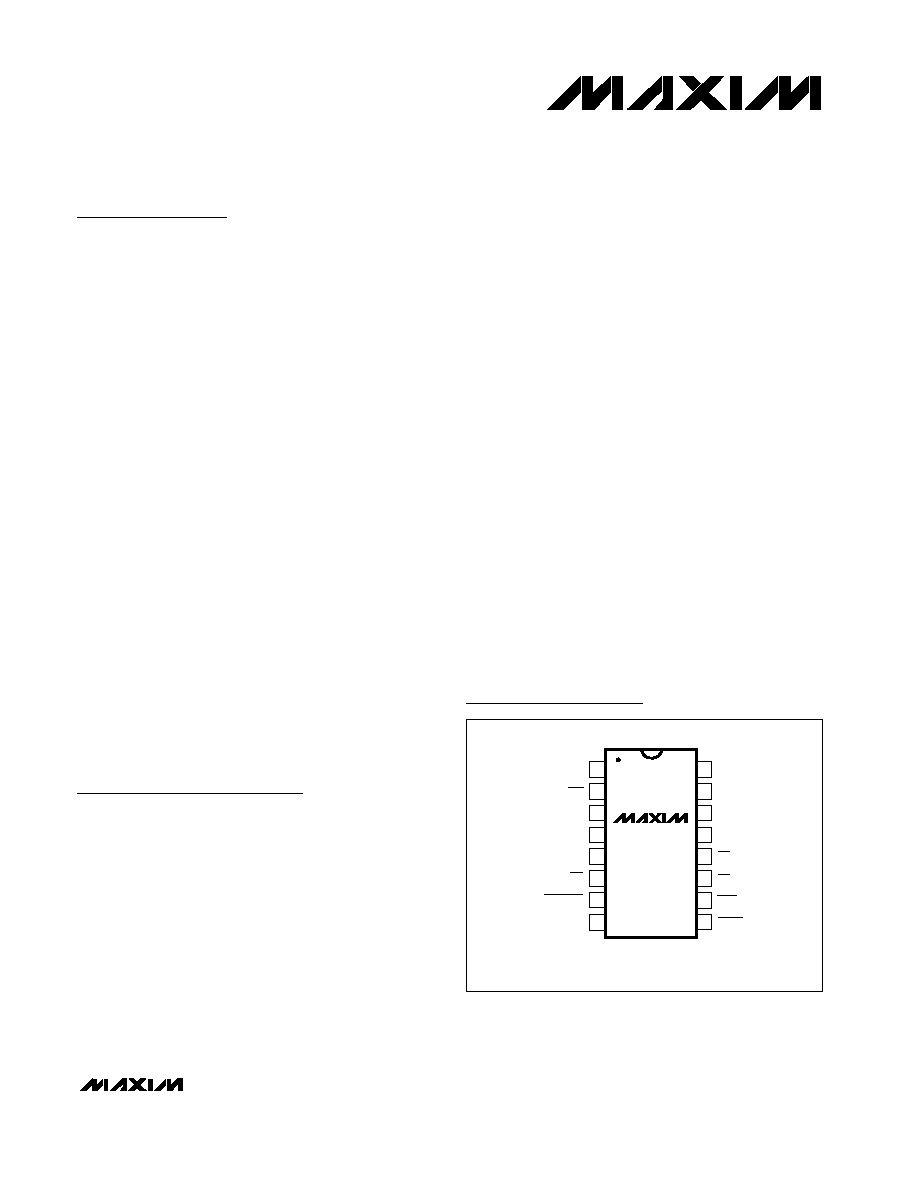
16
15
14
13
12
11
10
9
1
2
3
4
5
6
7
8
RESET
RESET
WDO
CE IN
GND
V
CC
OUT
BATT
TOP VIEW
MAX807
CE OUT
WDI
LOW LINE
MR
BATT OK
PFI
PFO
BATT ON
DIP/SO/TSSOP
Pin Configuration
Ordering Information and Typical Operating Circuit appear at end of data sheet.
SuperCap is a registered trademark of Baknor Industries. MaxCap is a registered trademark of Cesiwid, Inc.
For pricing, delivery, and ordering information, please contact Maxim/Dallas Direct! at
1-888-629-4642, or visit Maxim's website at www.maxim-ic.com.
MAX807L/M/N
Full-Featured µP Supervisory Circuit with
±1.5% Reset Accuracy
2
_______________________________________________________________________________________
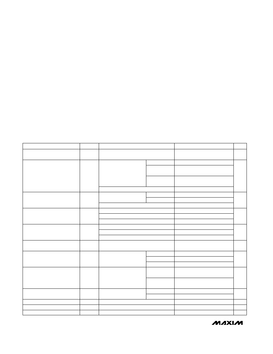
ABSOLUTE MAXIMUM RATINGS
ELECTRICAL CHARACTERISTICS
(V
CC
= 4.60V to 5.5V for the MAX807L, V
CC
= 4.50V to 5.5V for the MAX807N, V
CC
= 4.35V to 5.5V for the MAX807M,
V
BATT
= 2.8V, V
PFI
= 0V, T
A
= T
MIN
to T
MAX
. Typical values are tested with V
CC
= 5V and T
A
= +25∞C, unless otherwise noted.)
Stresses beyond those listed under "Absolute Maximum Ratings" may cause permanent damage to the device. These are stress ratings only, and functional
operation of the device at these or any other conditions beyond those indicated in the operational sections of the specifications is not implied. Exposure to
absolute maximum rating conditions for extended periods may affect device reliability.
Input Voltages (with respect to GND)
V
CC
..........................................................................-0.3V to 6V
V
BATT
.......................................................................-0.3V to 6V
All Other Inputs......................................-0.3V to (V
OUT
+ 0.3V)
Input Current
V
CC
Peak ...........................................................................1.0A
V
CC
Continuous .............................................................500mA
I
BATT
Peak......................................................................250mA
I
BATT
Continuous .............................................................50mA
GND .................................................................................50mA
All Other Inputs ................................................................50mA
Continuous Power Dissipation (T
A
= +70∞C)
Plastic DIP (derate 10.53mW/∞C above +70∞C) ..........842mW
Wide SO (derate 9.52mW/∞C above +70∞C)................762mW
CERDIP (derate 10.00mW/∞C above +70∞C) ...............800mW
TSSOP (derate 6.70 mW/∞C above +70∞C) .................533mW
Operating Temperature Ranges
MAX807_C_E ......................................................0∞C to +70∞C
MAX807_E_E ...................................................-40∞C to +85∞C
MAX807_MJE ................................................-55∞C to +125∞C
Storage Temperature Range .............................-65∞C to +160∞C
Lead Temperature (soldering, 10s) .................................+300∞C
V
BATT
= 2.8V, V
CC
= 3.0V
V
CC
= 0V, V
BATT
= 2.8V
V
CC
= 3V, I
OUT
= 100mA
V
CC
= 4.5V,
I
OUT
= 250mA
V
BATT
= 2.0V, I
OUT
= 5mA, V
CC
= 0V
V
BATT
= 2.8V, I
OUT
= 10mA, V
CC
= 0V
V
BATT
= 4.5V, I
OUT
= 20mA, V
CC
= 0V
CONDITIONS
µA
-1.0
1.0
BATT Standby Current (Note 3)
-0.1
0.1
µA
50
Supply Current in Battery-
Backup Mode (excludes I
OUT
)
(Note 2)
5
0.4
1
µA
70
110
Supply Current in Normal
Operating Mode (excludes I
OUT
)
V
V
BATT
- 0.20 V
BATT
- 0.08
V
OUT
in Battery-Backup Mode
V
BATT
- 0.25 V
BATT
- 0.12
V
BATT
- 0.17
1.2
2.5
V
CC
to OUT On-Resistance
1.8
1.0
1.4
UNITS
MIN
TYP
MAX
SYMBOL
PARAMETER
V
0
5.5
Operating Voltage Range
V
BATT
, V
CC
(Note 1)
MAX807C/E
MAX807M
V
BATT
= 2.0V, I
OUT
= 5mA
V
BATT
= 2.8V, I
OUT
= 10mA
V
BATT
= 4.5V, I
OUT
= 20mA
16
40
BATT to OUT On-Resistance
12
25
8.5
T
A
= +25∞C
MAX807C/E
MAX807M
T
A
= +25∞C
T
A
= T
MIN
to
T
MAX
V
BATT
= 2.8V
Power up
Power down
V
V
BATT
Battery-Switchover Threshold
V
BATT
+ 0.05
V
CC
= 3V, V
BATT
= 2.8V, I
OUT
= 100mA
V
CC
= 4.5V
V
CC
- 0.02
I
OUT
= 25mA
I
OUT
= 250mA,
MAX807C/E
I
OUT
= 250mA,
MAX807M
V
OUT
in Normal Operating
Mode
V
V
CC
- 0.25 V
CC
- 0.12
V
CC
- 0.35 V
CC
- 0.22
V
CC
- 0.45
mV
0.1
0.4
Battery-Switchover Hysteresis
50
BATT ON Output, Low Voltage
V
RST (max)
, I
SINK
= 3.2mA
V
2
2.7
BATT ON Output, High Voltage
V
CC
= 0V, I
SOURCE
= 0.1mA, V
BATT
= 2.8V
V
V
IH
MAX807L/M/N
Full-Featured µP Supervisory Circuit with
±1.5% Reset Accuracy
_______________________________________________________________________________________
3
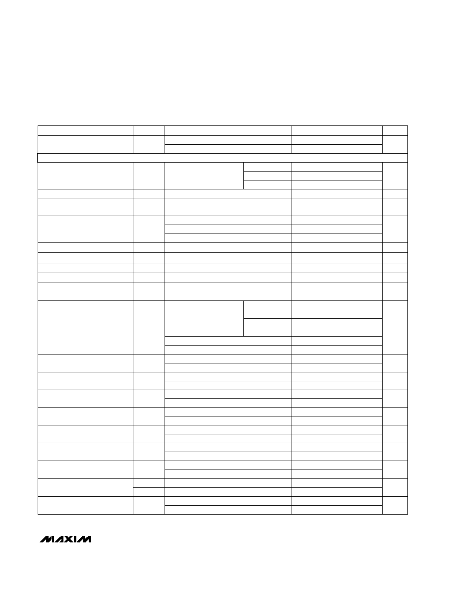
ELECTRICAL CHARACTERISTICS (continued)
(V
CC
= 4.60V to 5.5V for the MAX807L, V
CC
= 4.50V to 5.5V for the MAX807N, V
CC
= 4.35V to 5.5V for the MAX807M,
V
BATT
= 2.8V, V
PFI
= 0V, T
A
= T
MIN
to T
MAX
. Typical values are tested with V
CC
= 5V and T
A
= +25∞C, unless otherwise noted.)
CONDITIONS
UNITS
MIN
TYP
MAX
SYMBOL
PARAMETER
Sink current
70
4.600
4.675
4.750
V
5
BATT ON Output
Short-Circuit Current
Source current, V
CC
= 0V, V
BATT
= 2.8V
4.350
4.425
4.500
LOW LINE to RESET
Threshold Voltage
V
LR
Reset Threshold Hysteresis
V
CC
falling
30
52
70
mV
13
mV
4.500
4.575
4.650
V
RST
Reset Threshold
V
CC
rising and falling
4.63
4.71
MAX807N
V
CC
to LOW LINE Delay
V
CC
falling at 1mV/µs
24
µs
µs
26
V
CC
to RESET Delay
V
CC
falling at 1mV/µs
4.48
4.56
MAX807M
Minimum Watchdog Input
Pulse Width
Watchdog-Timeout Period
V
IL
= 0.8V, V
IH
= 0.75 x V
CC
t
WD
100
ns
V
1.12
1.6
2.24
s
ms
140
200
280
t
RP
RESET Active-Timeout Period
V
CC
rising
4.73
4.81
MAX807L
MAX807L
MAX807N
MAX807M
0.3
0.3
I
SINK
= 50µA,
V
BATT
= 0V, V
CC
falling
V
CC
- 1.5
V
CC
- 0.1
RESET Output Voltage
I
SOURCE
= 0.1mA
0.1
0.4
I
SINK
= 3.2mA, V
CC
= 4.25V
mA
60
Output sink current, V
CC
= 4.25V
1.6
I
SC
RESET Output
Short-Circuit Current
Output source current
V
CC
= 1V,
MAX807_C
V
CC
= 1.2V,
MAX807_E/M
V
0.4
I
SINK
= 3.2mA
V
CC
- 1.5
RESET Output Voltage
I
SOURCE
= 5mA
V
0.4
I
SINK
= 3.2mA, V
CC
= 4.25V
V
CC
- 1.5
LOW LINE Output Voltage
I
SOURCE
= 5mA
mA
60
Output sink current
15
I
SC
RESET Output
Short-Circuit Current
Output source current, V
CC
= 4.25V
mA
28
Output sink current, V
CC
= 4.25V
20
I
SC
LOW LINE Output
Short-Circuit Current
Output source current
V
0.4
I
SINK
= 3.2mA
V
CC
- 1.5
WDO Output Voltage
I
SOURCE
= 5mA
mA
mA
35
Output sink current
20
I
SC
WDO Output
Short-Circuit Current
Output source current
V
LL
V
LOW LINE Threshold,
V
CC
Rising
V
0.75 x V
CC
0.8
V
IH
WDI Threshold Voltage
(Note 4)
V
IL
µA
-50
-10
Reset deasserted, WDI = 0V
16
50
WDI Input Current
Reset deasserted, WDI = V
CC
RESET, LOW LINE, AND WATCHDOG TIMER
MAX807L/M/N
Full-Featured µP Supervisory Circuit with
±1.5% Reset Accuracy
4
_______________________________________________________________________________________
Note 1: Either V
CC
or V
BATT
can go to 0 if the other is greater than 2.0V.
Note 2: The supply current drawn by the MAX807 from the battery (excluding I
OUT
) typically goes to 15µA when (V
BATT
- 0.1V)
< V
CC
< V
BATT
. In most applications, this is a brief period as V
CC
falls through this region (see Typical Operating Characteristics).
Note 3: "+"= battery discharging current, "-"= battery charging current.
Note 4: WDI is internally connected to a voltage-divider between V
CC
and GND. If unconnected, WDI is driven to 1.8V (typical),
disabling the watchdog function.
Note 5: Overdrive (V
OD
) is measured from center of hysteresis band.
Note 6: The chip-enable resistance is tested with V
CE IN
= V
CC
/2, and I
CE IN
= 1mA.
Note 7: The chip-enable propagation delay is measured from the 50% point at CE IN to the 50% point at CE OUT.
ELECTRICAL CHARACTERISTICS (continued)
(V
CC
= 4.60V to 5.5V for the MAX807L, V
CC
= 4.50V to 5.5V for the MAX807N, V
CC
= 4.35V to 5.5V for the MAX807M,
V
BATT
= 2.8V, V
PFI
= 0V, T
A
= T
MIN
to T
MAX
. Typical values are tested with V
CC
= 5V and T
A
= +25∞C, unless otherwise noted.)
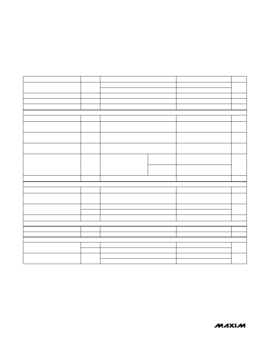
CONDITIONS
UNITS
MIN
TYP
MAX
SYMBOL
PARAMETER
PFI Leakage Current
±0.005
±40
nA
mV
20
PFI Hysteresis
µA
±0.00002
±1
CE IN Leakage Current
Disabled mode, MR = 0V
µs
14
PFI to PFO Delay (Note 5)
PFI Input Threshold
V
PFT
V
PFI
falling
2.22
2.285
2.35
V
2.20
2.265
2.33
RESET to CE OUT Delay
V
CC
falling
28
µs
75
150
CE IN to CE OUT Resistance
(Note 6)
Enabled mode, V
CC
= V
RST
(max)
MR Minimum Pulse Input
1
µs
ns
170
MR-to-RESET Propagation
Delay
mA
17
CE OUT Short-Circuit Current
(RESET Active)
V
CC
= 5V, disabled mode,
CE OUT = 0, MR = 0V
ns
2
8
CE IN to CE OUT
Propagation Delay (Note 7)
V
CC
= 5V, C
LOAD
= 50pF,
50
source impedance driver
V
3.5
CE OUT Output Voltage High
(RESET Active)
Disabled mode, MR = 0V
MR Threshold
V
IH
2.4
V
BATT OK Threshold
V
BOK
2.200
2.265
2.350
V
BATT OK Hysteresis
20
mV
Output Voltage
(PFO, BATT OK)
V
OL
I
SINK
= 3.2mA
0.4
V
Output Short-Circuit Current
I
SC
Output sink current
35
mA
V
PFI
rising
V
BATT
- 0.1
V
BATT
V
CC
= 5V,
I
OUT
= 2mA
V
CC
= 0V,
I
OUT
= 10µA
V
IL
0.8
V
OH
I
SOURCE
= 5mA
V
CC
- 1.5
Output source current
20
V
OD
= 30mV, V
PFI
falling
MR Pullup Current
MR = 0V
50
100
200
µA
CHIP-ENABLE GATING
MANUAL RESET INPUT
BATT OK COMPARATOR
LOGIC OUTPUTS
MAX807L/M/N
Full-Featured µP Supervisory Circuit with
±1.5% Reset Accuracy
_______________________________________________________________________________________
5
80
60
-60
-20
60
140
V
CC
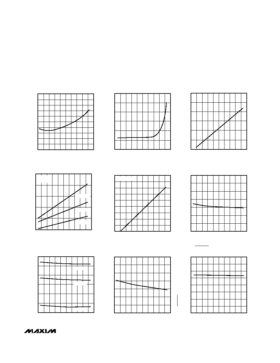
SUPPLY CURRENT vs. TEMPERATURE
(NORMAL OPERATING MODE)
64
76
MAX807-01
TEMPERATURE (∞C)
V
CC
SUPPLY CURRENT (
µ
A)
20
100
-40
40
120
0
80
72
68
62
66
78
74
70
3.0
2.5
2.0
1.5
1.0
0.5
0
-60
-20
60
140
BATTERY SUPPLY CURRENT vs.
TEMPERATURE (BATTERY-BACKUP MODE)
MAX807-02
TEMPERATURE (∞C)
BATTERY SUPPLY CURRENT (
µ
A)
20
100
-40
40
120
0
80
6
5
4
3
2
1
0
-60
-20
60
140
CHIP-ENABLE PROPAGATION DELAY
vs. TEMPERATURE
MAX807-03
TEMPERATURE (∞C)
PROPAGATION DELAY (ns)
20
100
-40
40
120
0
80
30
5
-60
-20
60
140
BATT-TO-OUT ON-RESISTANCE
vs. TEMPERATURE
10
25
MAX807-04
TEMPERATURE (
∞C)
BATT
-
TO
-
OUT
ON
-
RESISTANCE
(
)
20
100
-40
40
120
0
80
20
15
V
BATT
= 2.0V
V
BATT
= 2.8V
V
BATT
= 4.5V
V
CC
= 0V
I
OUT
= 10mA
4.70
4.65
4.60
4.55
4.50
4.45
4.40
-60
-20
60
140
RESET THRESHOLD
vs. TEMPERATURE
MAX807-07
TEMPERATURE (∞C)
RESET THRESHOLD (V)
20
100
-40
40
120
0
80
MAX807L
MAX807N
MAX807M
1.6
1.5
1.4
1.3
1.2
1.1
1.0
0.9
0.8
0.7
-60
-20
60
140
V
CC
-TO-OUT ON-RESISTANCE
vs. TEMPERATURE
MAX807-05
TEMPERATURE (∞C)
V
CC
-TO-OUT ON-RESISTANCE (
)
20
100
-40
40
120
0
80
I
OUT
= 250mA
2.340
2.320
2.300
2.280
2.260
2.240
2.220
2.200
-60
-20
60
140
PFI THRESHOLD
vs. TEMPERATURE (V
PFI
FALLING)
MAX807-06
TEMPERATURE (∞C)
PFI THRESHOLD (V)
20
100
-40
40
120
0
80
280
260
240
220
200
180
160
140
-60
-20
60
140
RESET TIMEOUT PERIOD
vs. TEMPERATURE (V
CC
RISING)
MAX807-08
TEMPERATURE (∞C)
RE
S
ET TIME
O
UT PERI
O
D
(
ms
)
20
100
-40
40
120
0
80
0
10
20
30
40
50
60
70
80
-60
-20
60
140
LOW LINE -TO-RESET THRESHOLD
vs. TEMPERATURE (V
CC
FALLING)
MAX807-09
TEMPERATURE (∞C)
LOW LINE-TO-RESET THRESHOLD (mV)
20
100
-40
40
120
0
80
__________________________________________Typical Operating Characteristics
(V
CC
= 5V, V
BATT
= 2.8V, PFI = 0, no load, T
A
= +25∞C, unless otherwise noted.)