
_______________General Description
The MAX817/MAX818/MAX819 microprocessor (µP)
supervisory circuits simplify power-supply monitoring,
battery control, and chip-enable gating in µP systems
by reducing the number of components required.
These devices are designed for use in +5V-powered
systems. Low supply current (11µA typical) and small
package size make these devices ideal for portable
applications. The MAX817/MAX818/MAX819 are specif-
ically designed to ignore fast transients on V
CC
. Other
supervisory functions include active-low reset, backup-
battery switchover, watchdog input, battery freshness
seal, and chip-enable gating. The
Selector Guide below
lists the specific functions available from each device.
These devices offer two pretrimmed reset threshold volt-
ages for ±5% or ±10% power supplies: 4.65V for the L
versions and 4.40V for the M versions. The MAX817/
MAX818/MAX819 are available in space-saving µMAX
packages, as well as 8-pin DIP/SO.
________________________Applications
Battery-Powered Computers and Controllers
Embedded Controllers
Intelligent Instruments
Critical µP Monitoring
Portable Equipment
____________________________Features
o
Precision Supply-Voltage Monitor:
4.65V (MAX81_L)
4.40V (MAX81_M)
o
11µA Quiescent Supply Current
o
200ms Reset Time Delay
o
Watchdog Timer with 1.6sec Timeout
(MAX817/MAX818)
o
Battery-Backup Power Switching; Battery Voltage
Can Exceed V
CC
o
Battery Freshness Seal
o
On-Board, 3ns Gating of Chip-Enable Signals
(MAX818)
o
Uncommitted Voltage Monitor for Power-Fail or
Low-Battery Warning (MAX817/MAX819)
o
Manual Reset Input (MAX819)
MAX817L/M, MAX818L/M, MAX819L/M*
+5V Microprocessor Supervisory Circuits
________________________________________________________________
Maxim Integrated Products
1
WDI
GND
PFO
PFI
1
2
8
7
BATT
RESET
V
CC
OUT
MAX817
DIP/SO/
µ
MAX
TOP VIEW
3
4
6
5
_________________Pin Configurations
19-0494; Rev 1; 3/96
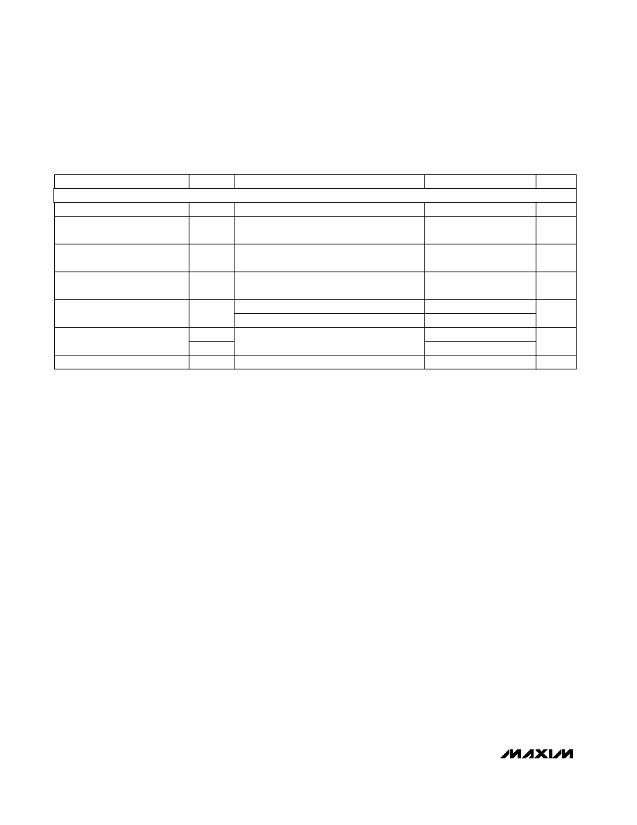
PART
MAX817
_CPA
MAX817_CSA
MAX817_CUA
0∞C to +70∞C
0∞C to +70∞C
0∞C to +70∞C
TEMP. RANGE
PIN-PACKAGE
8 Plastic DIP
8 SO
8 µMAX
______________Ordering Information
_____________________Selector Guide
Ordering Information continued on last page.
These parts offer a choice of reset threshold voltage. From the
table below, select the suffix corresponding to the desired
threshold and insert it into the blank to complete the part number.
For free samples & the latest literature: http://www.maxim-ic.com, or phone 1-800-998-8800
SUFFIX
RESET THRESHOLD (V)
L
4.65
M
4.40
FEATURE
MAX817
L/M
Active-Low Reset
Backup-Battery Switchover
MAX818
L/M
MAX819
L/M
Power-Fail Comparator
--
Watchdog Input
--
Battery Freshness Seal
Manual Reset Input
--
--
Chip-Enable Gating
--
Pin-Package
8-DIP/SO/
µMAX
8-DIP/SO/
µMAX
--
8-DIP/SO/
µMAX
Low-Power, Pin-
Compatible Upgrades for:
MAX690A/
MAX692A
--
MAX703/
MAX704
Typical Operating Circuit appears at end of data sheet.
Pin Configurations continued at end of data sheet.
*Patents Pending

MAX817L/M, MAX818L/M, MAX819L/M*
+5V Microprocessor Supervisory Circuits
2
_______________________________________________________________________________________
ABSOLUTE MAXIMUM RATINGS
ELECTRICAL CHARACTERISTICS
(V
CC
= +4.75V to +5.5V for MAX81_L, V
CC
= +4.5V to +5.5V for MAX81_M, V
BATT
= 2.8V, T
A
= T
MIN
to T
MAX
, unless otherwise
noted. Typical values are at T
A
= +25∞C.)
Stresses beyond those listed under "Absolute Maximum Ratings" may cause permanent damage to the device. These are stress ratings only, and functional
operation of the device at these or any other conditions beyond those indicated in the operational sections of the specifications is not implied. Exposure to
absolute maximum rating conditions for extended periods may affect device reliability.
Note 1:
The input voltage limits on PFI and WDI may be exceeded (up to 12V V
IN
) if the current into these pins is limited to less
than 10mA.
Input Voltage
V
CC
, BATT ..........................................................-0.3V to +6.0V
All Other Pins (Note 1).............................-0.3V to (V
CC
+ 0.3V)
Input Current
V
CC
Peak ..............................................................................1A
V
CC
Continuous .............................................................250mA
BATT Peak .....................................................................250mA
BATT Continuous .............................................................50mA
GND .................................................................................25mA
Output Current
OUT................................................................................250mA
All Other Outputs .............................................................25mA
OUT Short-Circuit Duration.................................................10sec
Continuous Power Dissipation (T
A
= +70∞C)
Plastic DIP (derate 9.09mW/∞C above +70∞C) .............727mW
SO (derate 5.88mW/∞C above +70∞C) ..........................471mW
µMAX (derate 4.10mW/∞C above +70∞C) .....................330mW
Operating Temperature Ranges
MAX81_ _C_A ......................................................0∞C to +70∞C
MAX81_ _E_A ...................................................-40∞C to +85∞C
Storage Temperature Range .............................-65∞C to +160∞C
Lead Temperature (soldering, 10sec) .............................+300∞C
As applicable;
CE IN = 0V,
WDI and
MR unconnected
V
CC
< V
RST
I
OUT
= 50mA
I
OUT
= 5mA
V
CC
= 0V, V
OUT
= 0V
I
OUT
= 250µA, V
CC
< (V
BATT
- 0.2V)
CONDITIONS
mV
40
Battery Switchover Hysteresis
mV
-20
Battery Switch Threshold
(V
CC
- V
BATT
)
20
V
V
BATT -
V
BATT -
0.1
0.02
V
OUT
in Battery-Backup Mode
µA
11
60
I
SUPPLY
Supply Current (excluding I
OUT
)
11
45
V
0
5.5
Operating Voltage Range, V
CC
,
V
BATT
(Note 2)
100
BATT to OUT On-Resistance
5
10
V
CC
to OUT On-Resistance
V
V
CC
- V
CC
-
0.5
0.25
V
OUT
Output
V
CC
- V
CC
-
0.05
0.025
µA
5.0
µA
1
BATT Leakage Current,
Freshness Seal Enabled
UNITS
MIN
TYP
MAX
SYMBOL
PARAMETER
V
CC
= 0V
Supply Current in Battery-
Backup Mode (excluding I
OUT
)
0.05
1.0
MAX81_ _C
MAX81_ _E
T
A
= +25∞C
T
A
= T
MIN
to
T
MAX
Power-up
Power-down
T
A
= +25∞C
T
A
= T
MIN
to
T
MAX
5.5V > V
CC
> (V
BATT
+ 0.2V)
BATT Standby Current (Note 3)
-0.10
0.02
µA
-1.00
0.02

ELECTRICAL CHARACTERISTICS (continued)
(V
CC
= +4.75V to +5.5V for MAX81_L, V
CC
= +4.5V to +5.5V for MAX81_M, V
BATT
= 2.8V, T
A
= T
MIN
to T
MAX
, unless otherwise
noted. Typical values are at T
A
= +25∞C.)
MAX817L/M, MAX818L/M, MAX819L/M*
+5V Microprocessor Supervisory Circuits
_______________________________________________________________________________________
3
V
P FO
= 0V
V
PFI
> 1.30V, I
SOURCE
= 40µA, V
CC
> 4.5V
MAX81_M
V
PFI
< 1.20V, I
SINK
= 3.2mA, V
CC
> 4.50V
MAX81_L
WDI = GND, time average
From V
RST
, V
CC
falling at 10V/ms
WDI = V
CC
, time average
V
CC
= 5V
MAX81_ _C, V
CC
= 1V, V
CC
falling,
V
BATT
= 0V, I
SINK
= 50µA
V
CC
> V
RST(MAX),
I
SOURCE
= 800µA
V
CC
< V
RST(MIN),
I
SINK
= 3.2mA
V
IL
= 0.4V, V
IH
= 0.8V
CC
CONDITIONS
µA
250
500
PFO Short-Circuit Current
V
CC
- 1.5
V
OH
PFO Output Voltage
V
0.4
V
OL
nA
-25
0.01
25
I
PFI
PFI Input Current
mV
4
PFI Input Hysteresis
V
1.20
1.25
1.30
V
PFT
PFI Input Threshold
µA
-20
-15
WDI Input Current (Note 5)
120
160
V
3.5
V
IH
WDI Input Threshold (Note 4)
0.8
V
IL
ns
50
t
WDI
WDI Pulse Width
V
4.25
4.40
4.50
V
RST
Reset Threshold
4.50
4.65
4.75
sec
1.00
1.60
2.25
t
WD
Watchdog Timeout Period
µs
100
V
CC
to
RESET Delay
0.3
mV
25
Reset Threshold Hysteresis
ms
140
200
280
t
RP
Reset Timeout Period
V
CC
- 1.5
V
OH
0.4
V
OL
UNITS
MIN
TYP
MAX
SYMBOL
PARAMETER
MAX81_ _E, V
CC
= 1.2V, V
CC
falling,
V
BATT
= 0V, I
SINK
= 100µA
V
0.3
RESET Output Voltage
0.8
V
2.0
V
IL
MR Input Threshold
µs
1
MR Pulse Width
V
IH
ns
100
MR Pulse that Would Not Cause
a Reset
ns
120
MR to Reset Delay
k
45
63
85
MR Pull-Up Resistance
RESET AND WATCHDOG TIMER
POWER-FAIL COMPARATOR (MAX817/MAX819 only)
MANUAL RESET INPUT (MAX819 only)
MAX817L/M, MAX818L/M, MAX819L/M*
+5V Microprocessor Supervisory Circuits
4
_______________________________________________________________________________________
ELECTRICAL CHARACTERISTICS (continued)
(V
CC
= +4.75V to +5.5V for MAX81_L, V
CC
= +4.5V to +5.5V for MAX81_M, V
BATT
= 2.8V, T
A
= T
MIN
to T
MAX
, unless otherwise
noted. Typical values are at T
A
= +25∞C.)
Power-down
V
CC
= 5V
I
OUT
= -1µA, V
CC
= 0V, V
BATT
= 2.8V
I
OUT
= -100µA, V
CC
= 0V
Enable mode
Disable mode
CONDITIONS
µs
15
RESET to CE OUT Delay
3.5
V
IL
CE OUT Input Threshold
V
0.8
V
IH
V
2.7
V
OH
CE OUT Output
V
CC
- 1V
40
150
CE IN to CE OUT Resistance
(Note 6)
µA
±0.005
±1
CE IN Leakage Current
UNITS
MIN
TYP
MAX
SYMBOL
PARAMETER
Note 2:
Either V
CC
or V
BATT
can go to 0V if the other is greater than 2.0V.
Note 3:
"-" = battery-charging current, "+" = battery-discharging current.
Note 4:
WDI is internally serviced within the watchdog timeout period if WDI is left unconnected.
Note 5:
WDI input is designed to be driven by a three-stated output device. To float WDI, the "high-impedance mode" of the output
device must have a maximum leakage current of 10µA and a maximum output capacitance of 200pF. The output device
must also be able to source and sink at least 200µA when active.
Note 6:
The chip-enable resistance is tested with V
CC
= +4.75V for the MAX818L and V
CC
= +4.5V for the MAX818M.
V
C E IN
= V
C E OUT
= V
CC
/2.
Note 7:
The chip-enable propagation delay is measured from the 50% point at
CE IN to the 50% point at CE OUT.
Disable mode,
CE OUT = 0V
mA
0.1
0.75
2.0
CE OUT Short-Circuit Current
(Reset Active)
50
source impedance driver, C
LOAD
= 50pF
ns
3
8
CE IN to CE OUT Propagation
Delay (Note 7)
CHIP-ENABLE GATING (MAX818 only)
MAX817L/M, MAX818L/M, MAX819L/M*
+5V Microprocessor Supervisory Circuits
_______________________________________________________________________________________
5
8
-40
40
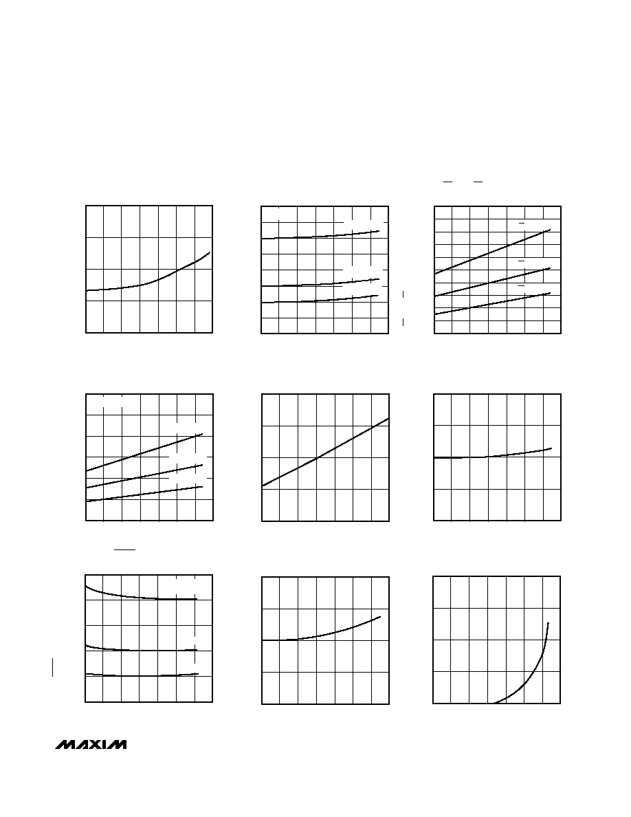
SUPPLY CURRENT
vs. TEMPERATURE (NO LOAD)
12
MAX817/18/19-01
TEMPERATURE (∞C)
SUPPLY CURRENT (
µ
A)
-20
0
20
80
100
60
16
14
10
0
-40
40
BATTERY SUPPLY CURRENT
(BACKUP MODE) vs. TEMPERATURE
20
80
100
120
140
160
MAX817/18/19-02
TEMPERATURE (∞C)
BATTERY SUPPLY CURRENT (nA)
-20
0
20
80
100
60
60
40
V
CC
= 0V
V
BATT
= 5.0V
V
BATT
= 2.8V
V
BATT
= 2.0V
0
-40
40
CE IN TO CE OUT ON-RESISTANCE
vs. TEMPERATURE
20
80
MAX817/18/19-03
TEMPERATURE (∞C)
CE IN TO CE OUT ON-RESISTANCE (
)
-20
0
20
80
100
60
60
40
90
100
10
70
50
30
V
CE IN
= 4V
V
CE IN
= 3V
V
CE IN
= 2V
0
-40
40
BATT TO OUT ON-RESISTANCE
vs. TEMPERATURE
MAX817/18/19-04
TEMPERATURE (∞C)
BATT TO OUT ON-RESISTANCE (
)
-20
0
20
80
100
60
50
100
150
200
250
300
V
BATT
= 2.0V
V
BATT
= 2.8V
V
BATT
= 5.0V
V
CC
= 0V
0
-40
40
V
CC
TO RESET PROPAGATION DELAY
vs. TEMPERATURE
200
MAX817/18/19-07
TEMPERATURE (∞C)
V
CC
TO RESET PROPAGATION DELAY (ms)
-20
0
20
80
100
60
300
400
500
100
V
CC
FALLING AT:
0.25V/ms
1V/ms
10V/ms
3
-40
40
V
CC
TO OUT ON-RESISTANCE
vs. TEMPERATURE
MAX817/18/19-05
TEMPERATURE (∞C)
V
CC
TO OUT ON-RESISTANCE (
)
-20
0
20
80
100
60
4
5
6
7
180
-40
40
RESET TIMEOUT PERIOD
vs. TEMPERATURE
MAX817/18/19-06
TEMPERATURE (∞C)
RESET TIMEOUT PERIOD (ms)
-20
0
20
80
100
60
190
200
210
220
1.50
-40
40
WATCHDOG TIMEOUT PERIOD
vs. TEMPERATURE
1.60
MAX817/18/19-08
TEMPERATURE (∞C)
WATCHDOG TIMEOUT PERIOD (sec)
-20
0
20
80
100
60
1.65
1.70
1.55
0
-40
40
BATTERY FRESHNESS SEAL
LEAKAGE CURRENT vs. TEMPERATURE
10
MAX817/18/19-09
TEMPERATURE (∞C)
LEAKAGE CURRENT (nA)
-20
0
20
80
100
60
15
20
5
__________________________________________Typical Operating Characteristics
(V
CC
= +5V, V
BATT
= 3.0V, T
A
= +25∞C, unless otherwise noted.)